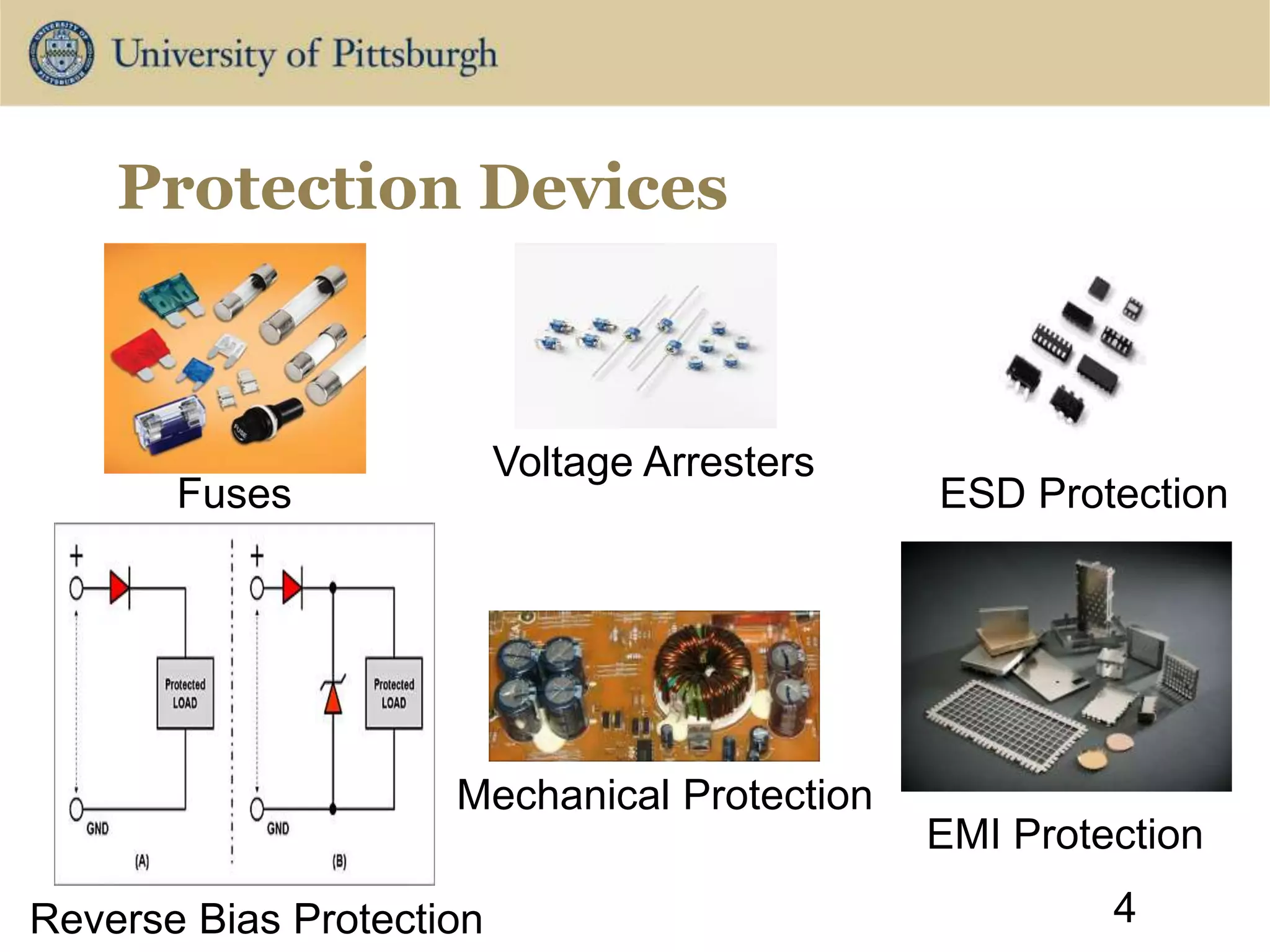
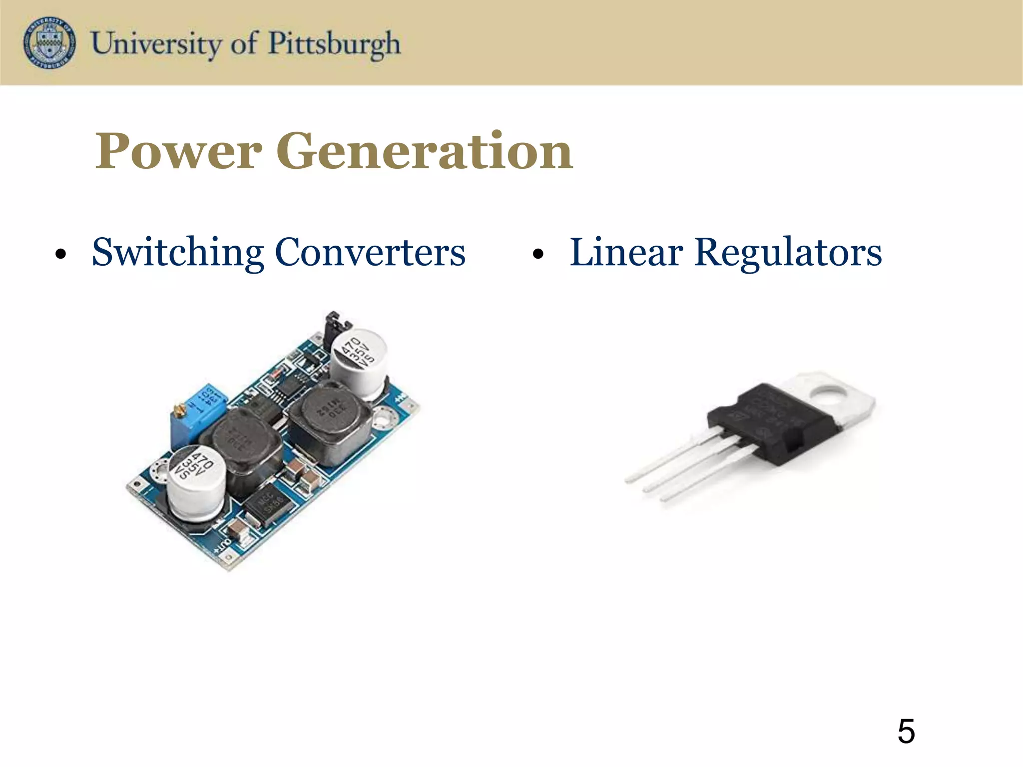
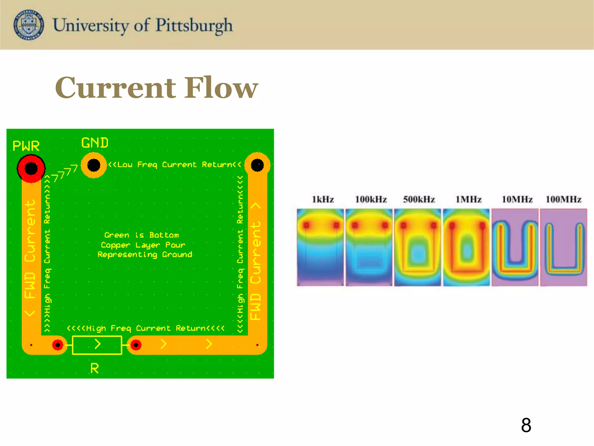
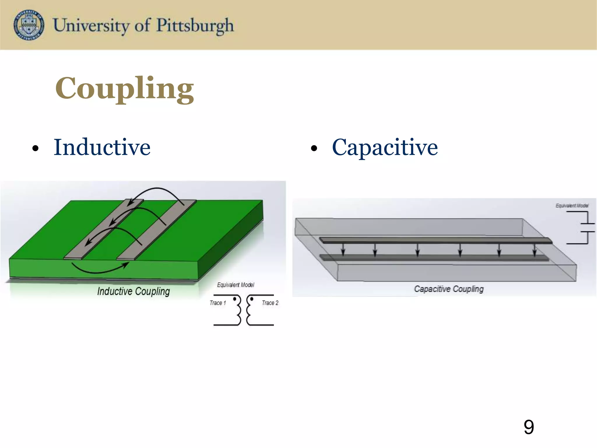
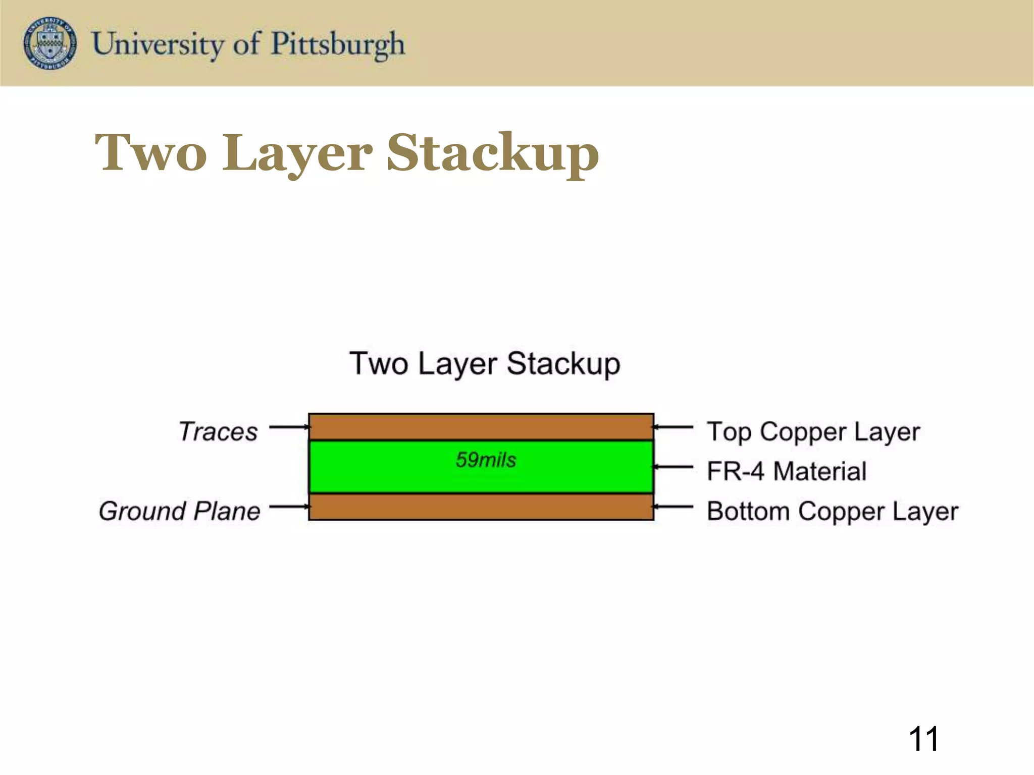
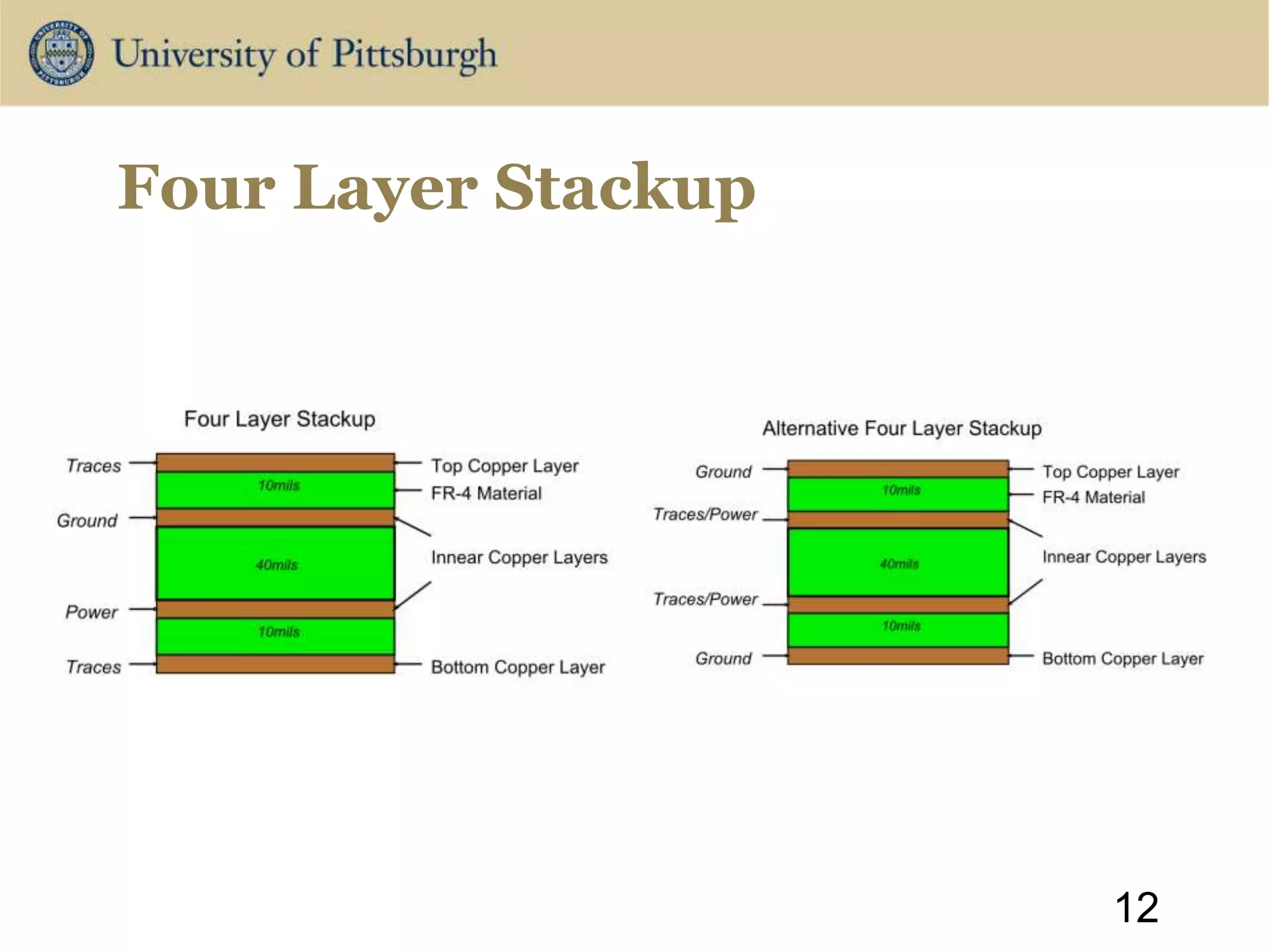
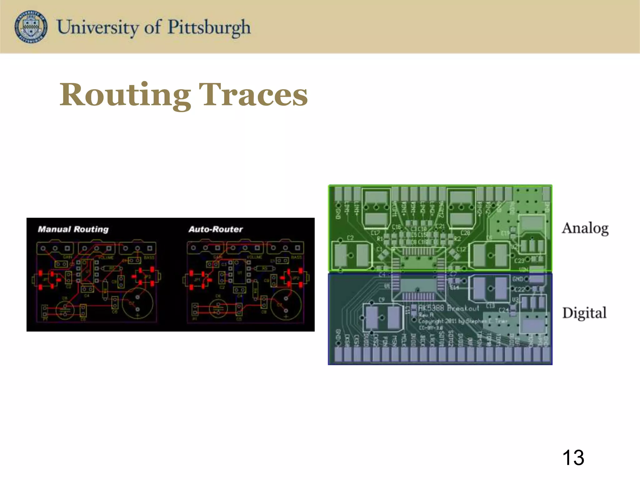
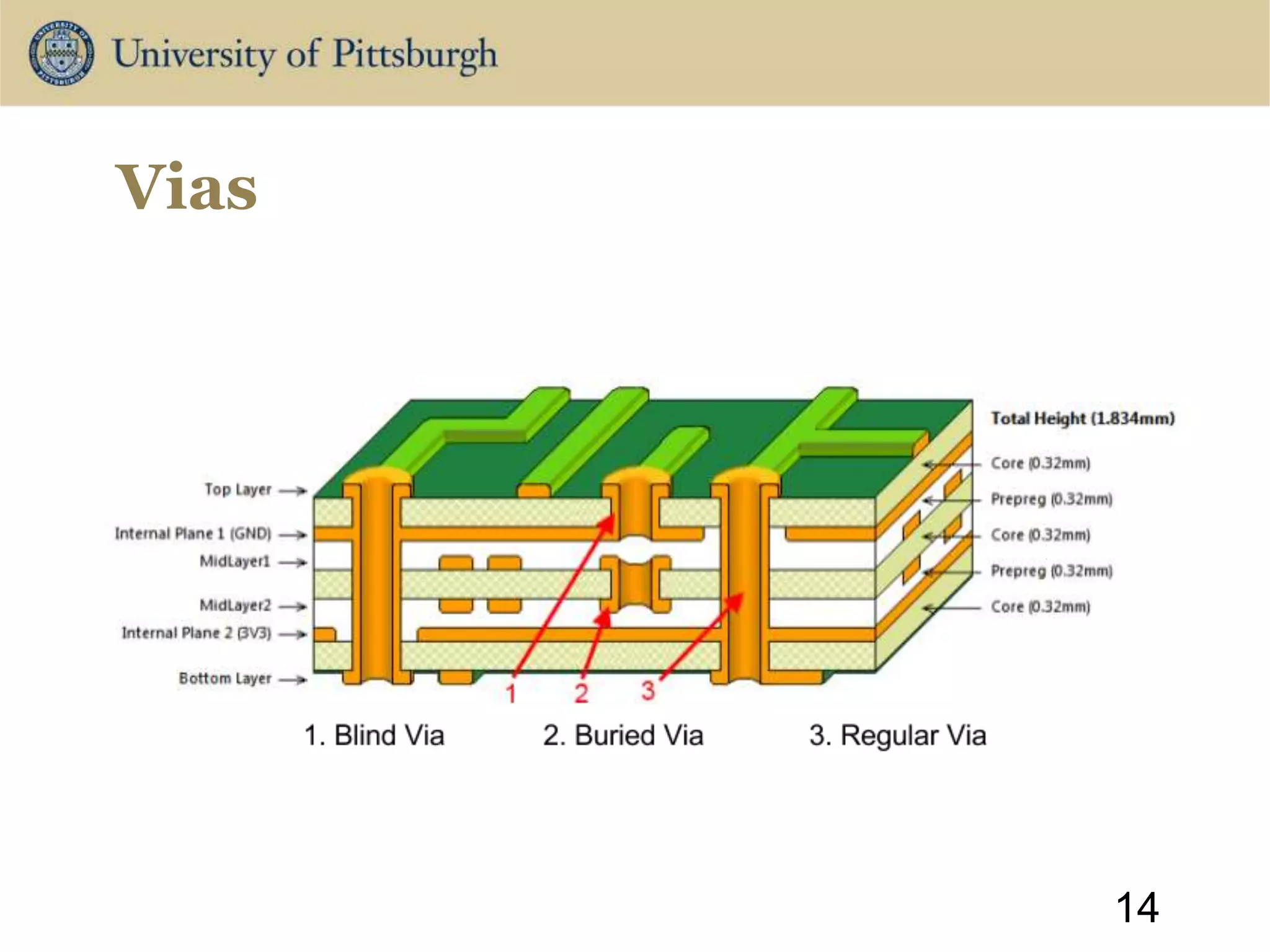
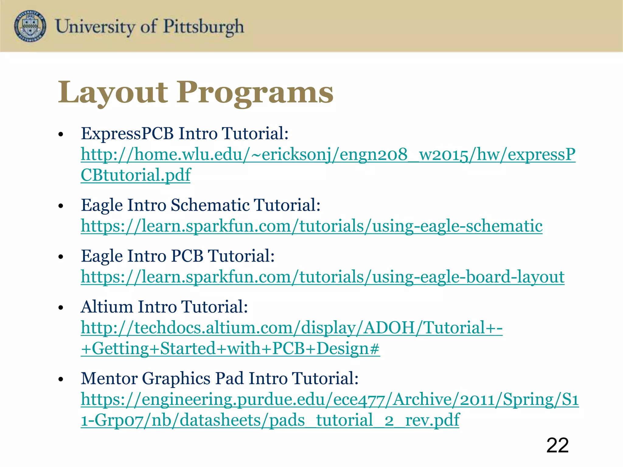
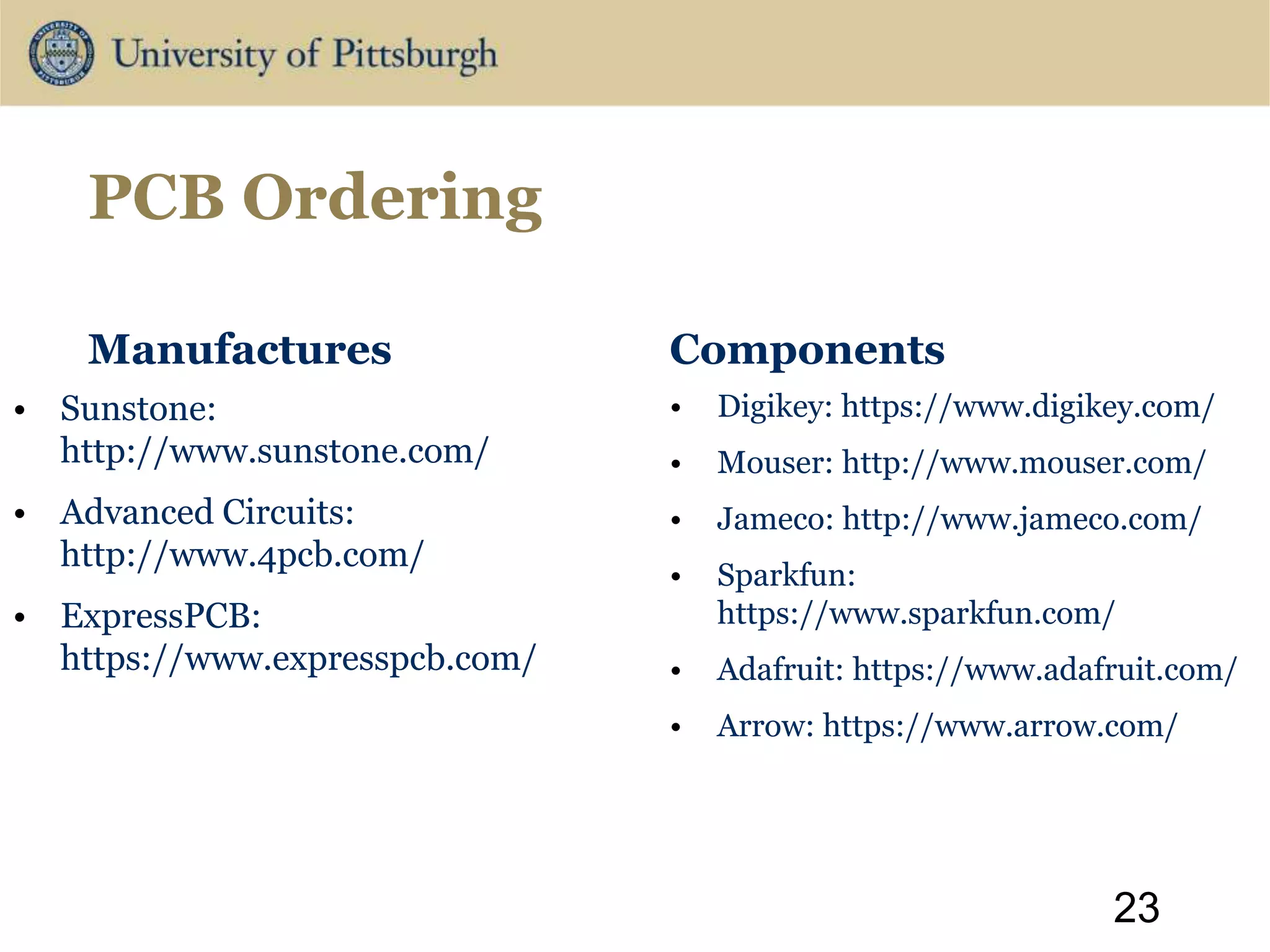
This document provides guidelines for PCB design, including key principles of current flow, coupling, and stackup goals. It discusses protection devices, power generation, routing traces, vias, copper pours, grounding, decoupling capacitors, component selection, circuit mounting, and layout programs. Manufacturers for PCB ordering are also listed.
A printed circuit board (PCB) mechanically supports and electrically connects electronic components using conductive tracks, pads and other features etched from copper sheets laminated onto a non-conductive substrate.
Creative Hi-Tech would like to share some basics of Printed Circuit Boards which will help you to gain some knowledge before going to any vendor. This power point presentation will clear your basic doubts regarding the PCB.
Designing process of printed circuit boardselprocus
Most key element in electronic circuits and equipment’s is the Printed Circuit Board which connects electronic components with conductive lines printed
Sorry to say but the college spelling is wrong actually "technology" word is missing. Its by mistake.
A presentation on printed circuit board designing. A brief discussion on pcb fabrication. Basic steps involved in it.
A class to introduce students to designing Printed Circuit Boards (PCBs) using the Eagle software. Reflow soldering with stencil and solder paste will also be covered. This class was originally held by me at One Maker Group.
The lesson should take approximately 6 hours to complete.
The example designs used in this class can be found in the repo here. https://github.com/yeokm1/intro-to-pcb-design-eagle
Grounding:
A conducting connection, whether intentional or accidental, bywhich an electric circuit or equipment is connected to the earth, or to someconducting body of relatively large extent that serves in place of the earth.
Grounded system:
A system of conductors in which at least one conductor or point (usually the middle wire or neutral point of transformer or generator windings) is intentionally grounded, either solidly or through an impedance.
Grounded solidly:
Connected directly through an adequate ground connection in which no impedance has been intentionally inserted.
Grounded effectively:
Grounded through a sufficiently low impedance such that for all system conditions the ratio of zero sequence reactance to positive sequence reactance (X0/X1) is positive and less than 3, and the ratio of zero sequence resistance to positive sequence reactance (R0/X1) is positive and less than 1.
This Lecture includes the Resistivity survey, field procedure, application advantage, limitaion, Apparant resistivity, VES (Vertical Electrical Sounding), Resistivity Profiling and IP Survey in brief.
Final project report on grocery store management system..pdfKamal Acharya
In today’s fast-changing business environment, it’s extremely important to be able to respond to client needs in the most effective and timely manner. If your customers wish to see your business online and have instant access to your products or services.
Online Grocery Store is an e-commerce website, which retails various grocery products. This project allows viewing various products available enables registered users to purchase desired products instantly using Paytm, UPI payment processor (Instant Pay) and also can place order by using Cash on Delivery (Pay Later) option. This project provides an easy access to Administrators and Managers to view orders placed using Pay Later and Instant Pay options.
In order to develop an e-commerce website, a number of Technologies must be studied and understood. These include multi-tiered architecture, server and client-side scripting techniques, implementation technologies, programming language (such as PHP, HTML, CSS, JavaScript) and MySQL relational databases. This is a project with the objective to develop a basic website where a consumer is provided with a shopping cart website and also to know about the technologies used to develop such a website.
This document will discuss each of the underlying technologies to create and implement an e- commerce website.
Sachpazis:Terzaghi Bearing Capacity Estimation in simple terms with Calculati...Dr.Costas Sachpazis
Terzaghi's soil bearing capacity theory, developed by Karl Terzaghi, is a fundamental principle in geotechnical engineering used to determine the bearing capacity of shallow foundations. This theory provides a method to calculate the ultimate bearing capacity of soil, which is the maximum load per unit area that the soil can support without undergoing shear failure. The Calculation HTML Code included.
Water scarcity is the lack of fresh water resources to meet the standard water demand. There are two type of water scarcity. One is physical. The other is economic water scarcity.
Explore the innovative world of trenchless pipe repair with our comprehensive guide, "The Benefits and Techniques of Trenchless Pipe Repair." This document delves into the modern methods of repairing underground pipes without the need for extensive excavation, highlighting the numerous advantages and the latest techniques used in the industry.
Learn about the cost savings, reduced environmental impact, and minimal disruption associated with trenchless technology. Discover detailed explanations of popular techniques such as pipe bursting, cured-in-place pipe (CIPP) lining, and directional drilling. Understand how these methods can be applied to various types of infrastructure, from residential plumbing to large-scale municipal systems.
Ideal for homeowners, contractors, engineers, and anyone interested in modern plumbing solutions, this guide provides valuable insights into why trenchless pipe repair is becoming the preferred choice for pipe rehabilitation. Stay informed about the latest advancements and best practices in the field.
NO1 Uk best vashikaran specialist in delhi vashikaran baba near me online vas...Amil Baba Dawood bangali
Contact with Dawood Bhai Just call on +92322-6382012 and we'll help you. We'll solve all your problems within 12 to 24 hours and with 101% guarantee and with astrology systematic. If you want to take any personal or professional advice then also you can call us on +92322-6382012 , ONLINE LOVE PROBLEM & Other all types of Daily Life Problem's.Then CALL or WHATSAPP us on +92322-6382012 and Get all these problems solutions here by Amil Baba DAWOOD BANGALI
#vashikaranspecialist #astrologer #palmistry #amliyaat #taweez #manpasandshadi #horoscope #spiritual #lovelife #lovespell #marriagespell#aamilbabainpakistan #amilbabainkarachi #powerfullblackmagicspell #kalajadumantarspecialist #realamilbaba #AmilbabainPakistan #astrologerincanada #astrologerindubai #lovespellsmaster #kalajaduspecialist #lovespellsthatwork #aamilbabainlahore#blackmagicformarriage #aamilbaba #kalajadu #kalailam #taweez #wazifaexpert #jadumantar #vashikaranspecialist #astrologer #palmistry #amliyaat #taweez #manpasandshadi #horoscope #spiritual #lovelife #lovespell #marriagespell#aamilbabainpakistan #amilbabainkarachi #powerfullblackmagicspell #kalajadumantarspecialist #realamilbaba #AmilbabainPakistan #astrologerincanada #astrologerindubai #lovespellsmaster #kalajaduspecialist #lovespellsthatwork #aamilbabainlahore #blackmagicforlove #blackmagicformarriage #aamilbaba #kalajadu #kalailam #taweez #wazifaexpert #jadumantar #vashikaranspecialist #astrologer #palmistry #amliyaat #taweez #manpasandshadi #horoscope #spiritual #lovelife #lovespell #marriagespell#aamilbabainpakistan #amilbabainkarachi #powerfullblackmagicspell #kalajadumantarspecialist #realamilbaba #AmilbabainPakistan #astrologerincanada #astrologerindubai #lovespellsmaster #kalajaduspecialist #lovespellsthatwork #aamilbabainlahore #Amilbabainuk #amilbabainspain #amilbabaindubai #Amilbabainnorway #amilbabainkrachi #amilbabainlahore #amilbabaingujranwalan #amilbabainislamabad
Immunizing Image Classifiers Against Localized Adversary Attacksgerogepatton
This paper addresses the vulnerability of deep learning models, particularly convolutional neural networks
(CNN)s, to adversarial attacks and presents a proactive training technique designed to counter them. We
introduce a novel volumization algorithm, which transforms 2D images into 3D volumetric representations.
When combined with 3D convolution and deep curriculum learning optimization (CLO), itsignificantly improves
the immunity of models against localized universal attacks by up to 40%. We evaluate our proposed approach
using contemporary CNN architectures and the modified Canadian Institute for Advanced Research (CIFAR-10
and CIFAR-100) and ImageNet Large Scale Visual Recognition Challenge (ILSVRC12) datasets, showcasing
accuracy improvements over previous techniques. The results indicate that the combination of the volumetric
input and curriculum learning holds significant promise for mitigating adversarial attacks without necessitating
adversary training.
About
Indigenized remote control interface card suitable for MAFI system CCR equipment. Compatible for IDM8000 CCR. Backplane mounted serial and TCP/Ethernet communication module for CCR remote access. IDM 8000 CCR remote control on serial and TCP protocol.
• Remote control: Parallel or serial interface.
• Compatible with MAFI CCR system.
• Compatible with IDM8000 CCR.
• Compatible with Backplane mount serial communication.
• Compatible with commercial and Defence aviation CCR system.
• Remote control system for accessing CCR and allied system over serial or TCP.
• Indigenized local Support/presence in India.
• Easy in configuration using DIP switches.
Technical Specifications
Indigenized remote control interface card suitable for MAFI system CCR equipment. Compatible for IDM8000 CCR. Backplane mounted serial and TCP/Ethernet communication module for CCR remote access. IDM 8000 CCR remote control on serial and TCP protocol.
Key Features
Indigenized remote control interface card suitable for MAFI system CCR equipment. Compatible for IDM8000 CCR. Backplane mounted serial and TCP/Ethernet communication module for CCR remote access. IDM 8000 CCR remote control on serial and TCP protocol.
• Remote control: Parallel or serial interface
• Compatible with MAFI CCR system
• Copatiable with IDM8000 CCR
• Compatible with Backplane mount serial communication.
• Compatible with commercial and Defence aviation CCR system.
• Remote control system for accessing CCR and allied system over serial or TCP.
• Indigenized local Support/presence in India.
Application
• Remote control: Parallel or serial interface.
• Compatible with MAFI CCR system.
• Compatible with IDM8000 CCR.
• Compatible with Backplane mount serial communication.
• Compatible with commercial and Defence aviation CCR system.
• Remote control system for accessing CCR and allied system over serial or TCP.
• Indigenized local Support/presence in India.
• Easy in configuration using DIP switches.
3. Important Datasheet Info
• Pinout and Pin Orientation
• Package Size and Type
• Power Rating
• Soldering Temperatures
• Recommended Configurations
3
7. Key Principles
• How current flows through the board and its return pathway to ground
with changes in frequency.
• Traces can cause unwanted inductance or capacitance depending on how
they are laid out.
• Electric and magnetic field coupling and its propagation around traces
and planes and how these fields couple into surrounding traces/planes.
• Amount of current and voltage that is on traces and how that changes the
propagation of the EM fields from the trace or how the trace is affected
by outside radiation. The smaller the signal on the trace the more
susceptible to outside radiation it is. While a high current or very large
signal can cause very large EM wave propagation that creates noise on
surrounding ground planes and traces.
7
10. PCB Stackup Goals
1. A signal layer should always be adjacent to a ground or power plane. This
means placing the ground or power plane one layer below or on the same layer
as the trace is being run. This allows for return current to be as close to the
source as possible.
2. Signal layers should be tightly coupled to their adjacent planes. This means
keeping the ground plane close to the signal plane either above or below.
3. Power and Ground planes should always be closely coupled together. This
means placing the planes within one or two layers of each other.
4. High speed signals (>500MHz) should be routed on buried layers located
between planes. In this way the planes can act as shields and contain the
radiation from the high speed traces.
5. Multiple ground planes are very advantageous, since they will lower the ground
(reference plane) impedance of the board and reduce common mode radiation.
10
Once a design has been successfully proven through simulation and prototyping on a breadboard it is time to transition it to a PCB.
Pinout and Pin Orientation: Ensuring that the schematic model and PCB package model have the correct pinout for the part that is going to be used is very important. Sometime the exact same IC or part will come in a variety of different packages and pin orientations depending on the component.
Package Size and Type: ICs and passive components usually have both through hole and surface mount packaging available. It is important that the same exact part in the schematic is what will be on the physical PCB.
Power rating (P=IV): Depending on the design, there may be some components that heat dissipation is required for. If this is the case, space for a heatsink may need to be incorporated into the PCB design. Tools such as ANSYS IcePack and SIwave can perform thermal simulations to see if heatsinks are required.
Reflow Profiles: Reflow profiles describe how the component will be soldered to the PCB and what is the maximum soldering temperature that the component can handle. If hand soldering is to be performed it is easier if the components are placed on the top side of the board only. If the board is to be outsourced and assembled by a manufacturer like Advanced Circuit, components can be placed on both sides of the board. If reflow profiles are ignored and the part exceeds its thermal ratings, manufactures will often not replace the part.
Additional external components: Often times an IC or other component cannot just be placed on a PCB by itself. Additional capacitors and resistors are usually required and these components should be simulated and placed in the schematic to ensure proper function. A recommended configuration is sometimes included in the datasheet.
Fuses are devices that prevent too much current from going into a circuit. In general, at least one fuse should be included in a circuit on either the positive or negative terminal of the main voltage source. If there are several voltage sources on one board, include a fuse on each positive terminal. Fuses are one time use devices and must be replaced if they blow. There are several styles with the main two being quick blow and slow blow. Quick blow fuses open as soon as there is an overcurrent situation, even if it is for short period of time. Slow blow fuses will not open with quick pulses of high current, only with sustained high current.
Voltage Arresters or surge arresters are devices that prevent large overshoots in voltage applied to a circuit. This is important if higher voltages are capable of being seen on the circuit. A company called LittleFuse makes both voltage arresters and ESD protection devices.
Electrostatic Discharge (ESD) protection devices are extremely important for protecting a circuit from outside connections for any type of port included on the device such as USB, DVI, 3.5mm audio, and ethernet. ESD devices often incorporate transient voltage suppression (TVS) diodes.
Reverse Bias protection diodes are small circuits that in off chance that the voltage polarity to the circuit is connected incorrectly, it will not be destroyed. A reverse bias diode allows current to pass under normal circuit operation, but will stop current flow if the input voltage polarity is switched. The parallel Zener diode provides load dump suppression for inductive loads like a motor or alternator.
Mechanical Protection can also be included on the circuit in the form of rubber washers for vibration dampening, “RTV” or silicone elastomer adhesive for making large components more rigid, and epoxy coating over all components for weather and humidity resistance.
Electromagnetic Interference protection can also be included with a metal shield around certain components connected to ground that acts as a faraday cage.
Switching DC-DC Converters: Switching DC-DC converters are power electronic devices that can increase (boost) or decrease (buck) the input DC voltage to another DC voltage. These devices use a combination of transistors, diodes, capacitors, and inductors and can be found as self contained circuits. The devices are extremely power efficient and can provide greater variety of voltage outputs. Some disadvantages of these devices is that there is voltage and current ripple on the output of the device due to its switching nature. If the application is very voltage or noise sensitive a very high quality switching converter should be used or a linear regulator should be selected.
Linear Voltage regulators: Linear voltage regulators are also power electronic devices but they usually come in a three pin TO-220 package. This type of voltage converter is very easy to add into a PCB design and can be chosen to output a fixed voltage level or be tuned using some external resistors. This devices are usually very inefficient because they work essentially be absorbing any excess power coming into the device and turning it into heat. The devices will often require heatsinking especially if there is a large (~5V) difference between input and output voltages. The output voltage however will be very smooth because these devices are solid state and do not operate by switching.
PCB design depends on many factors but the design constraints change depending on what frequency the board is designed to operate around. The lower the frequency, the more relaxed the design guidelines become. Low frequency is approximately defined as being in the 100kHz ranges and below. Medium frequency is in the upper kHz and lower MHz ranges up to around 1MHz. Higher frequency is 10MHz and above into GHz regions. In analog design frequency refers to the fundamental frequency or frequency range that the board is expected to operate in. In digital design the frequency of the board is highly dependant on the rise time of the square wave digital signal and not as much on the fundamental frequency itself. The rise time can create extremely high frequency harmonics that affect how the circuit will operate.
Current usually moves through the path of least resistance, which in general and at lower frequencies is true. However, as frequency increases the electric and magnetic fields have a stronger effect and cause the return current to follow the trace back instead of following the shortest distance path to ground. This effect can cause noise and high frequency ringing on the ground plane that can be modeled with an RL series combination in the circuit schematic on the ground return path.
Traces and planes are large conductors that have an electric potential and electric current flowing over them which causes them to have an electromagnetic field that surrounds them. This EM field can radiate and couple into other parts of the circuit, causing noise.
Traces and planes can form either inductors or capacitors depending on how they are laid out and therefore can introduce undesirable impedance changes and coupling into the circuit. A trace running next to another trace on the same layer is essentially two parallel wires forming an inductor. As the trace width decreases the DC resistance as well as the inductance of the trace increases. A trace running over top of a ground plane or another trace is essentially a parallel plate capacitor. To limit the capacitive coupling, the traces can be run perpendicular to each other so surface area overlap is minimized. As the trace width increases over the ground plane the capacitance increases. These effects can be modeled with RL, RC, or RLC combinations in the circuit schematic. Typically the resistance, inductance, and capacitance these effects add is very small (pico or nano range) but as frequency increases it can make a big difference.
One goal of PCB layout is making the circuit as compact as possible but sometimes proper spacing between components and traces is required. Depending on how high the voltage or current on the PCB is will change how much spacing is needed to limit the EM coupling. For example if there is a very sensitive signal on the PCB that's 10mils wide and there is a trace that has 5A on it running right next to the sensitive signal that is 100mils wide with only 20mils spacing between them. There will be significant coupling of noise from the 5A trace into the sensitive signal trace due to inductive coupling. In order to limit that noise, it is a good idea to leave at least 2 to 3 high current trace widths of separation between the two traces, so in this case 300mil separation for 1oz/ft2 copper.
Two layer board designs are the most common for simple projects and prototyping because they are easy to manufacture and simple to design. In general the bottom layer is entirely filled with copper and chosen to act as the ground plane. The FR-4 material between the two layers is often set to be approximately 59mil which is the industry standard. Signal traces are then run along the top copper layer. In order to maintain a low impedance ground plane for return currents it is important to maximize the copper area of the ground plane by minimizing any routing that will interrupt sections of the ground plane.
On more complicated circuits, more than two copper layers may be necessary. Layers can be added in increments of two. Each additional copper layer is separated by a layer of FR-4. For most designs, four copper layers are sufficient with the inner layers being power and ground and the outer layers being used for traces. This stackup is adequate for most designs but only satisfies the first objective with keeping signal layers next to current return planes. An alternative stackup uses the outside layers for ground and the inner layers for traces and power planes. This stackup provides a very low impedance path to ground because of two ground layers (be sure to stitch the two ground layers together with vias to ensure they are both at the same potential). It also satisfies objectives 1, 2, 4, and 5. On four layer boards it is possible to do mixed analog and digital design but can be more challenging depending on the number of traces that is required to be routed. If space is running low for traces, ground planes, power planes and the design is starting to suffer it may be beneficial to increase the number of layers.
If a double sided board is being designed this stackup or the 6 layer stackup provides better noise isolation between components on either side. This means that a higher voltage power supply could be designed for the bottom layer and sensitive measurement devices can be designed for the top layer and be largely unaffected. The inner ground and copper planes provide good protection from stray EM radiation.
Traces can be “ratsnested” which autoroutes the connections between components while abiding by any trace rules that were set up in the program.
The length of the trace between individual components should try be kept to an absolute minimum. Traces that run around the entire perimeter of the PCB should be avoided at all costs.
For digital signals is is very important that the trace signals are the same exact length otherwise two signals (like clock and data) can reach the same place on the board at different times.
Sometimes traces seem to need to overlap with one another. At this point you'll need to place vias in your circuit and route the trace to another layer of the board to make the connections. If a trace crosses over another trace or touches in any way on the same layer it will make an electrical connection. For through hole components the hole for the lead can be used as a via for routing a trace to the other layer of the board. For highly sensitive signals it is important to try to avoid having too many vias (more than 2) because passing through different layers can cause noise to couple into the signal.
The minimum distance between traces is limited by the PCB manufacture and should be looked up before laying out a board with traces that are too close together. For most manufactures a rule of thumb distance is 7mil (0.007”) or 8mil (0.008”) minimum trace spacing, but it is good practice to look up the manufactures specifications before designing. Often a “snap-to-grid” feature of 0.05” works well for general board layout.
A wider trace will allow more current to flow without creating excessive heat.
Trace routing directions is usually limited to horizontal, vertical, or 45o angles. Sharp right angle turns should be avoided and replaced with two 45o bends with a short leg in between them.
Vias can have essentially 3 different types of electrical connections: disconnected, connected, thermal. A disconnected via will not make an electrical connection to any surrounding copper pour but can be connected to a trace or left entirely disconnected. A connected via will make an electrical connection to a surrounding copper pour. These electrical connections can be selective as to which layer of the board the via is connected to. A thermal connection will make electrical connection to a surrounding copper pour but will be connected with “spokes” around the pad and not solidly filled in. This can make soldering easier because the spokes limit the amount of heat that can be wicked into the copper pour away from the pad. For high current applications the spokes can also act as small fuses.
Two special types of vias called blind and buried can also be made that do not penetrate all the layers of a board but there are usually increased costs and special manufacturing techniques required to create them.
When vias are used in a board, care must be taken to not use too many so that they break up the ground plane. The ground plane should be kept as continuous as possible so that current is allowed to flow in the path of least resistance.
Copper pours are large areas of copper on the board that are often used for power and ground planes. Copper pours can also be used as “traces” for signals that need higher current carrying capabilities.
For designs that utilize ground planes that also exist on trace layers, “islands” can form in areas where there is high trace density. Islands are areas of copper that are isolated from the rest of the ground plane and do not make any electrical connection. These can lead to floating nodes and does not offer a return path to ground if a trace is accidentally connected to it. These can be removed from a plane by creating a “keep-out” area around high density traces.
A “star” ground topology comes from the notion that all points in a star emanate from a single common point, usually the power source. This is accomplished by connecting each component or IC’s ground pin individually to the power sources return current path.
For PCB’s that involve digital and analog components, there is usually a ground plane dedicated for each. This is done because analog devices are usually very sensitive to any noise on the ground plane the switching of digital signals can create a lot of high frequency noise. However, both planes must remain at the same potential so a star ground is usually done right at the power source to connect the two ground planes. This is the only connection between both planes in the board.
Modeling of current path to ground is often done with a very small resistance and inductance that can be present on both the digital and analog ground paths.
Vias can be used to “stitch” the ground planes together so that there is always a low impedance path and everything is kept at the same potential.
Sometimes on IC’s there is a very sensitive signal line running very close to the IC’s power line which can cause a significant amount of noise and coupling due to high current. A “guard trace” which is a trace connect to ground can be run surrounding the sensitive trace so that any noise developed by the power line is absorbed by ground.
n IC’s it is important to ensure that coupled noise from the power supply lines does not enter the the component because it can lead to unpredictable behavior. On a DC bus, a capacitor acts like an open circuit that only allows AC signals through. A decoupling capacitor is used to provide a low impedance path to ground for noise from a DC bus.
Often times in power supply regulator schematics a capacitor between the input power and ground and output power and ground will be shown, with no reference to wire length connecting the capacitor. If one considers how a decoupling capacitor works, it becomes apparent that the parasitic inductance of the the element will affect the response of the decoupling capacitor. For this reason it is highly discouraged the use of through hole capacitors for decoupling. It is the best practice to keep the capacitor leads and connecting traces as short as possible between the power and ground leads of the decoupling capacitor.
Rules of Thumb: All surface mount passives
Resistors: Carbon Film
Capacitors: Ceramic
Inductors: Depends, Multilayer
IC’s: Surface mount (less parasitic inductance from lead length)
Buy at least 2 to 3 extra spares for each component
On most boards mounts are taken care of by incorporating a large vias in each corner of the PCB. If standard standoffs are to be used the hole is usually 2.75mm and the pad is 6mm. Care must be taken not to put the hole too close to the edge of the board otherwise there will not be enough material to hold it and it can break, 2mm to 3mm is usually sufficient.
The mounting hole is a via and can be either left separated from a ground plane or connected. If connected to a ground plane, it allow for probes to be easily connected to the circuits ground from off a standoff. It also allows for many boards to be stacked together (like an Arduino Shield) and for all of them to share the same reference ground. These mounting holes allow for an EMI shield to also be attached if necessary. If left unconnected it allows the board to float above whatever surface it is on electrically. A compromise between the two design methodologies. Instead of directly connecting the mounting hole to ground it can be connected through a parallel RC circuit using a 1MΩ resistor an 10pF capacitor. This offers some ESD protection of the circuit.
Listed in learning curve from least challenging to most
Tutorials Given
Additional Programs
Saturn PCB Design Toolkit:
The Saturn PCB toolkit is handy calculation tool for calculating conductor impedance, thermal properties, via properties, digital signal trace impedances, and other board properties. This program saves a lot of time instead of doing all of these calculations by hand.
AppCAD:
If RF, Microwave, or wireless designs are being performed another handy toolkit is Avago Technologies AppCAD. AppCAD provides many circuit design calculations for antennas, amplifiers, filters, and transmission lines.