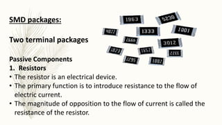
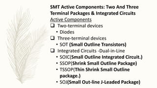
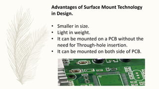
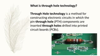
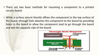
Surface Mount Devices
Presented by: S. S. Amale
M.Tech (Electronics)
An SMD, or surface mounted device, is an
electronic component that you would find on a
board. An SMT, or surface mount technology, is
the method of placing components (like an SMD)
on the board. In electronic manufacturing
services, the SMT process often works with SMDs
• What is the difference between SMT and
SMD?
• Surface Mount Device/components are very small as compared to
normal electronics components like resistor, capacitor etc.
• Surface Mount Device is specially designed for the integration of the
circuit i.e to make the circuit as small as possible.
• Integrated Circuit (IC) is the example of the SMD components, if you
open datasheet of any IC you can see the circuit diagram of that
particular IC
Step’s involved in assembly technique in SMT
https://www.sparkfun.com/marcomm/SFE03-0010-KitCard-SolderingSMD-ReaderSpreads.pdf
Soldering and Desoldering steps
involved in SMTs
SMD packages:
Two terminal packages
Passive Components
1. Resistors
• The resistor is an electrical device.
• The primary function is to introduce resistance to the flow of
electric current.
• The magnitude of opposition to the flow of current is called the
resistance of the resistor.
• A larger resistance value indicates a
greater opposition to current flow.
• The resistance is measured in ohms.
• The various uses of resistors are
setting biases, controlling gain, fixing
time constants, matching and loading
circuits, voltage division, and heat
generation.
2. Capacitors
• An electrical device capable of storing electrical energy and
releasing it at some predetermined rate at some
predetermined time.
• It consists essentially of two conducting surfaces
(electrodes) separated by an insulating material or
dielectric.
• A capacitor stores electrical energy, blocks the flow of
direct current, and permits the flow of alternating current
3. Inductors
• Inductors are also available in chip
form.
• However, you can not realize large
values of chip inductors as it is
practically available
• A typical chip inductor is shown
below:
SMT Active Components: Two And Three
Terminal Packages & Integrated Circuits
Active Components
 Two-terminal devices
• Diodes
 Three-terminal devices
• SOT (Small Outline Transistors)
 Integrated Circuits -Dual-in-Line
• SOIC(Small Outline Integrated Circuit.)
• SSOP(Shrink Small Outline Package)
• TSSOP(Thin Shrink Small Outline
package.)
• SOJ(Small Out-line J-Leaded Package)
Material Package Name Pin Count Pitches (mm)
Plastic
SOP (Small Out-line L-
Leaded Package)
8,16 1.27
24,28,32,40,44 1.0
SSOP (Shrink Small
Out-line L-Leaded
Package)
20 0.95
30,32,60,64,70 0.8
60 0.65
TSOP (1) (Thin Small
Out-line L-Leaded
Package)
32,40 0.5
TSOP (2) (Thin Small
Out-line L-Leaded
Package)
26/20,26/24,28/24,28,
32,
44/40,44,48,50/44,50,
54,66,70/64,70,86
1.27
1.27
0.8
0.65
0.5
QFP (Quad Flat L-
Leaded Package)
44,56,64,80,100,128,
160,208,240,272,304
1.0
44,56 0.8
64,80,100 0.65
Advantages of Surface Mount Technology
in Design.
• Smaller in size.
• Light in weight.
• It can be mounted on a PCB without the
need for Through-hole insertion.
• It can be mounted on both side of PCB.
What is through hole technology?
Through Hole technology is a method for
constructing electronic circuits in which the
pin-through hole (PTH) components are
inserted through holes drilled into printed
circuit boards (PCBs).
• There are two basic methods for mounting a component to a printed
circuits board.
• While a surface mount literally affixes the component to the top surface of
the board, through hole attaches the component to the board by providing
holes in the board to allow the component lead to go through the board
and exit the opposite side of the board.
• It has higher switching speed for its operation.
• It has high package density of components.
• It requires low storage area and volume and
hence it is very compact.
• It has no leads hence reduces the parasitic
inductance, capacitance, series resistance.
• It has very high resistance to mechanical
shock and vibrations.
Disadvantages
• The cost of SMD’s are higher than
those of their leaded counterparts.
• Smaller size of SMD’s ,makes manual
assembly much more difficult and
unreliable.
• It requires high accuracy in PCB
artwork and fabrication.
• The layout design of SMD ‘s are very
complex.
• It suffers from thermal problems
due to high packing density.
• The repair of electronic circuits with
SMDs is more complex.
Thank you!

Surface mount Devices(SMD)

  • 1.
    Surface Mount Devices Presentedby: S. S. Amale M.Tech (Electronics)
  • 2.
    An SMD, orsurface mounted device, is an electronic component that you would find on a board. An SMT, or surface mount technology, is the method of placing components (like an SMD) on the board. In electronic manufacturing services, the SMT process often works with SMDs • What is the difference between SMT and SMD?
  • 3.
    • Surface MountDevice/components are very small as compared to normal electronics components like resistor, capacitor etc. • Surface Mount Device is specially designed for the integration of the circuit i.e to make the circuit as small as possible. • Integrated Circuit (IC) is the example of the SMD components, if you open datasheet of any IC you can see the circuit diagram of that particular IC
  • 4.
    Step’s involved inassembly technique in SMT
  • 5.
  • 6.
    SMD packages: Two terminalpackages Passive Components 1. Resistors • The resistor is an electrical device. • The primary function is to introduce resistance to the flow of electric current. • The magnitude of opposition to the flow of current is called the resistance of the resistor.
  • 7.
    • A largerresistance value indicates a greater opposition to current flow. • The resistance is measured in ohms. • The various uses of resistors are setting biases, controlling gain, fixing time constants, matching and loading circuits, voltage division, and heat generation.
  • 8.
    2. Capacitors • Anelectrical device capable of storing electrical energy and releasing it at some predetermined rate at some predetermined time. • It consists essentially of two conducting surfaces (electrodes) separated by an insulating material or dielectric. • A capacitor stores electrical energy, blocks the flow of direct current, and permits the flow of alternating current
  • 9.
    3. Inductors • Inductorsare also available in chip form. • However, you can not realize large values of chip inductors as it is practically available • A typical chip inductor is shown below:
  • 10.
    SMT Active Components:Two And Three Terminal Packages & Integrated Circuits Active Components  Two-terminal devices • Diodes  Three-terminal devices • SOT (Small Outline Transistors)  Integrated Circuits -Dual-in-Line • SOIC(Small Outline Integrated Circuit.) • SSOP(Shrink Small Outline Package) • TSSOP(Thin Shrink Small Outline package.) • SOJ(Small Out-line J-Leaded Package)
  • 12.
    Material Package NamePin Count Pitches (mm) Plastic SOP (Small Out-line L- Leaded Package) 8,16 1.27 24,28,32,40,44 1.0 SSOP (Shrink Small Out-line L-Leaded Package) 20 0.95 30,32,60,64,70 0.8 60 0.65 TSOP (1) (Thin Small Out-line L-Leaded Package) 32,40 0.5 TSOP (2) (Thin Small Out-line L-Leaded Package) 26/20,26/24,28/24,28, 32, 44/40,44,48,50/44,50, 54,66,70/64,70,86 1.27 1.27 0.8 0.65 0.5 QFP (Quad Flat L- Leaded Package) 44,56,64,80,100,128, 160,208,240,272,304 1.0 44,56 0.8 64,80,100 0.65
  • 13.
    Advantages of SurfaceMount Technology in Design. • Smaller in size. • Light in weight. • It can be mounted on a PCB without the need for Through-hole insertion. • It can be mounted on both side of PCB.
  • 14.
    What is throughhole technology? Through Hole technology is a method for constructing electronic circuits in which the pin-through hole (PTH) components are inserted through holes drilled into printed circuit boards (PCBs).
  • 15.
    • There aretwo basic methods for mounting a component to a printed circuits board. • While a surface mount literally affixes the component to the top surface of the board, through hole attaches the component to the board by providing holes in the board to allow the component lead to go through the board and exit the opposite side of the board.
  • 16.
    • It hashigher switching speed for its operation. • It has high package density of components. • It requires low storage area and volume and hence it is very compact. • It has no leads hence reduces the parasitic inductance, capacitance, series resistance. • It has very high resistance to mechanical shock and vibrations.
  • 17.
    Disadvantages • The costof SMD’s are higher than those of their leaded counterparts. • Smaller size of SMD’s ,makes manual assembly much more difficult and unreliable. • It requires high accuracy in PCB artwork and fabrication.
  • 18.
    • The layoutdesign of SMD ‘s are very complex. • It suffers from thermal problems due to high packing density. • The repair of electronic circuits with SMDs is more complex.
  • 19.