Brief about PCBDesign
PCB – Printed Circuit Board
PCB is the main key for all the emerging Electronic Smart world.
PCB acts as a bridge between the various components with the help
of tracks, pads and lines incorporated in a laminated copper sheet.
PCB`s are classified majorly by its layers Single, Double and
Multiple.
PCB reduces Time, working Space, Error and cost of the product.
12.
PCB Evolution
1925: CharlessDucas, an American inventor, he stencils conductive
materials onto a flat wooden board.
1936: Paul Eisler develops the first printed circuit board to use in a radio set.
1943: Eisler patents a more advanced PCB design, glass-reinforced, non-
conductive substrate.
1948: The United States Army releases PCB technology to the public,
prompting widespread development.
2000s: PCBs have become smaller, lighter, much higher layer counts and
more complex.
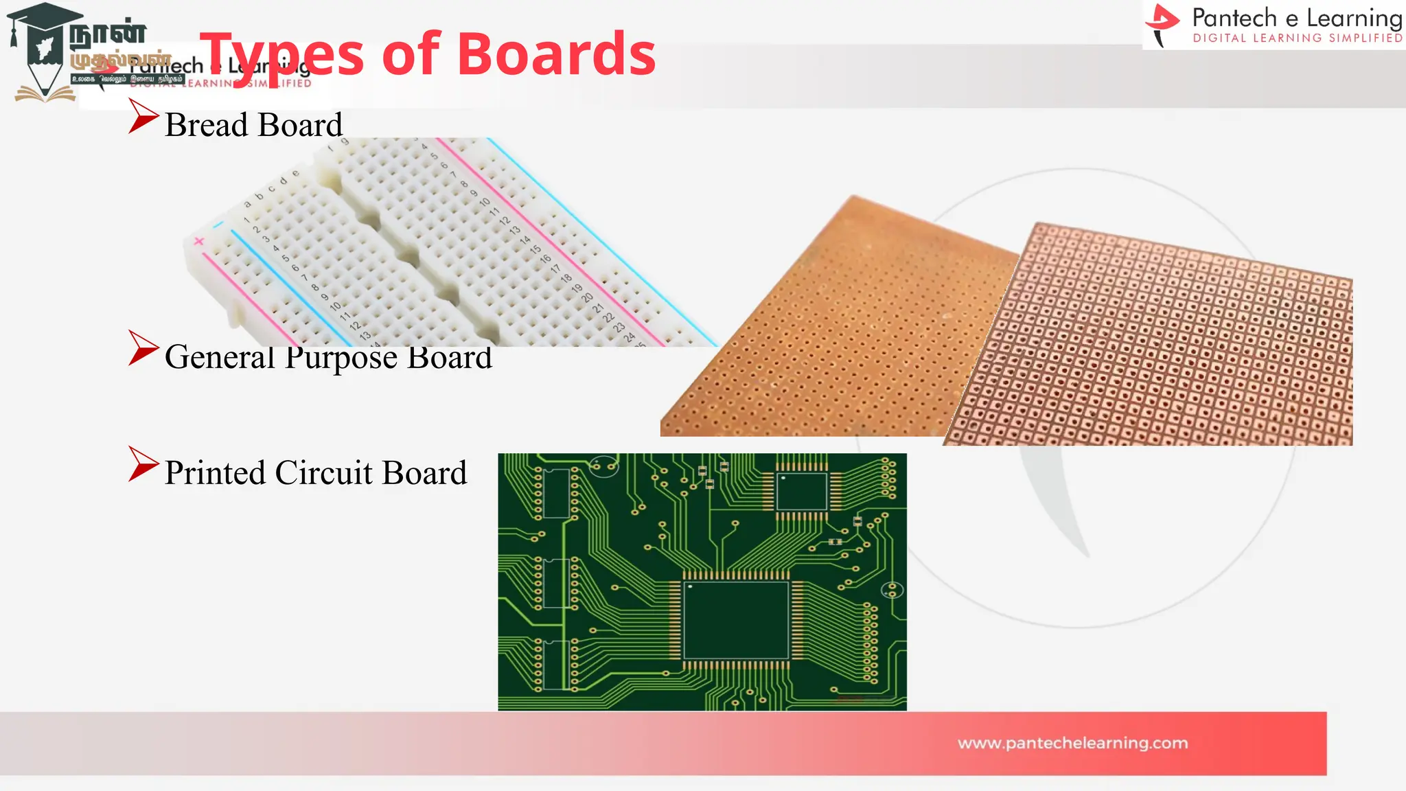
Layers or Materialin PCB`s
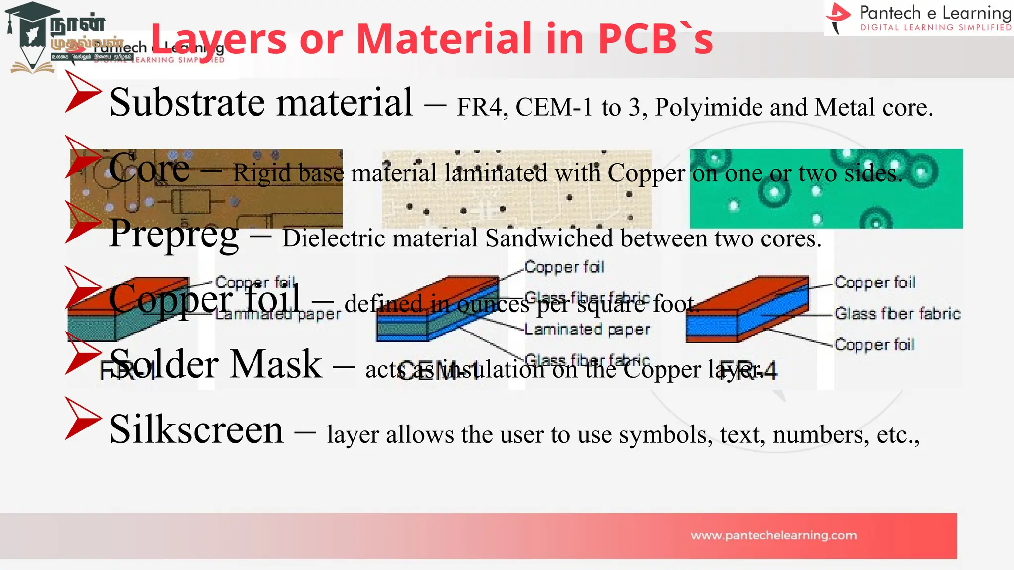
Substrate material – FR4, CEM-1 to 3, Polyimide and Metal core.
Core – Rigid base material laminated with Copper on one or two sides.
Prepreg – Dielectric material Sandwiched between two cores.
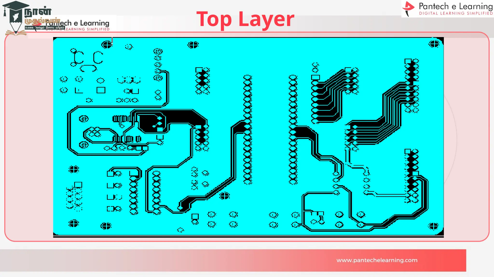
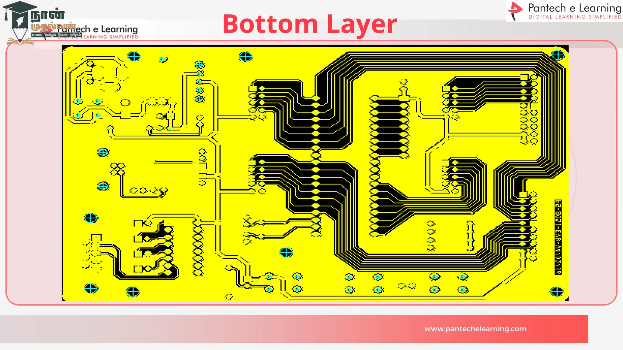
Copper foil – defined in ounces per square foot.
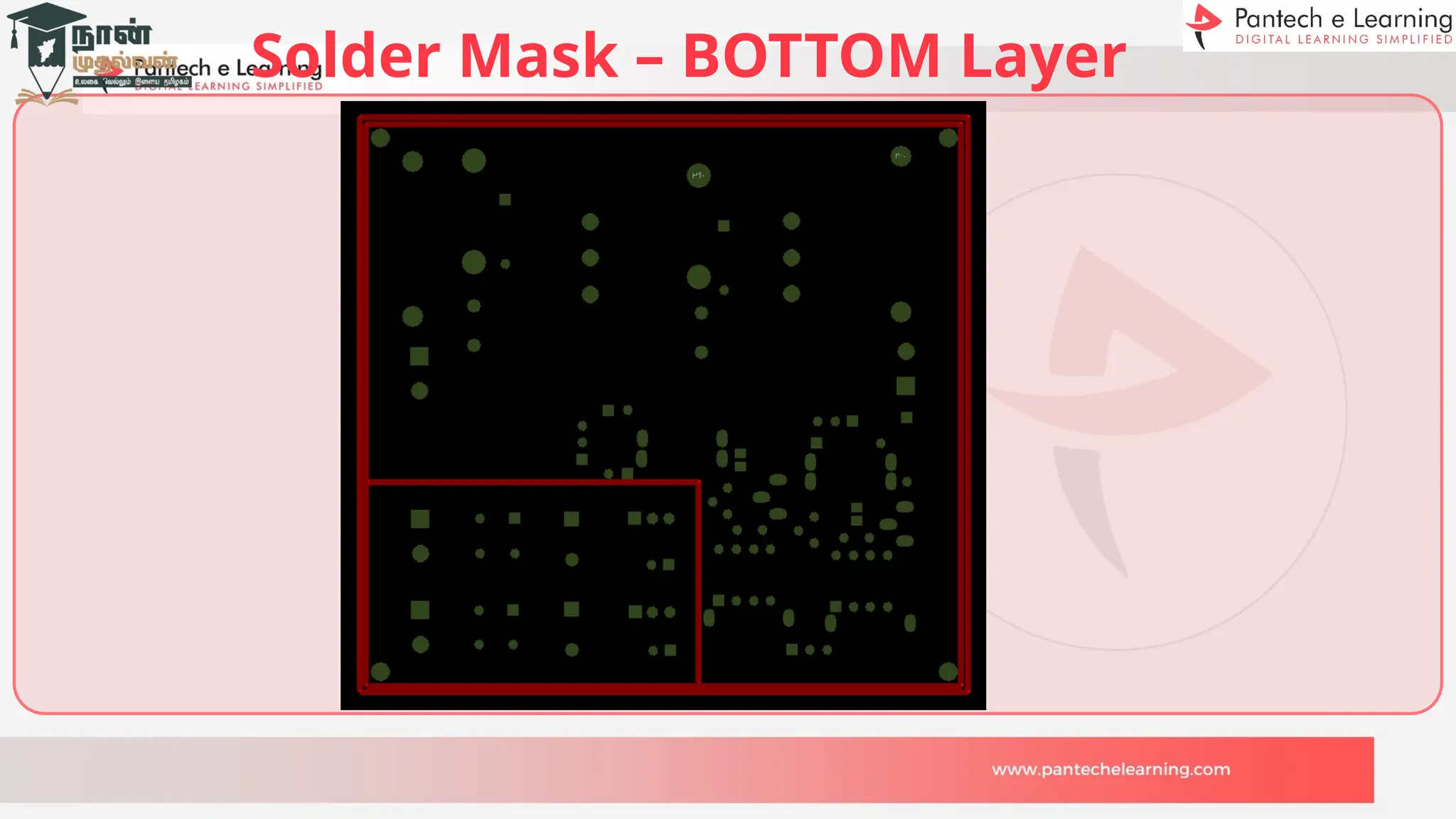
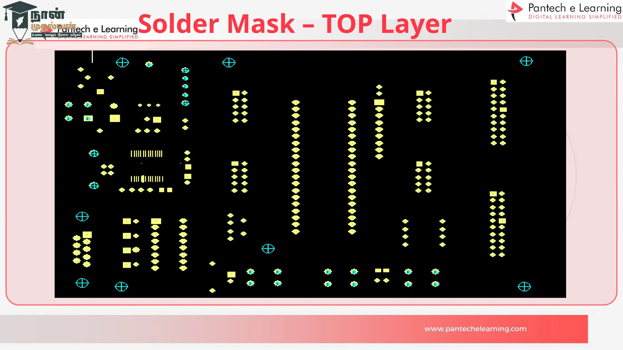
Solder Mask – acts as insulation on the Copper layer.
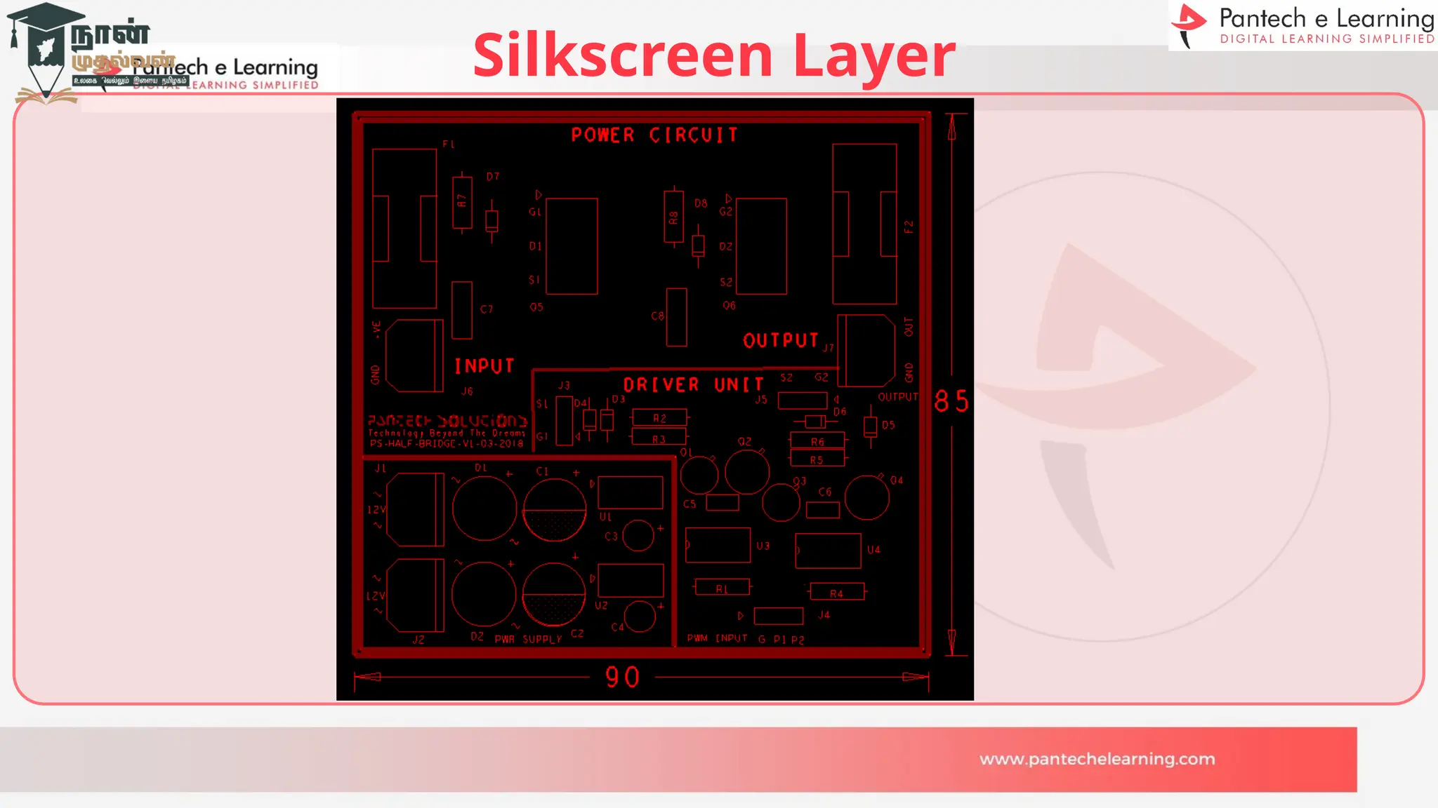
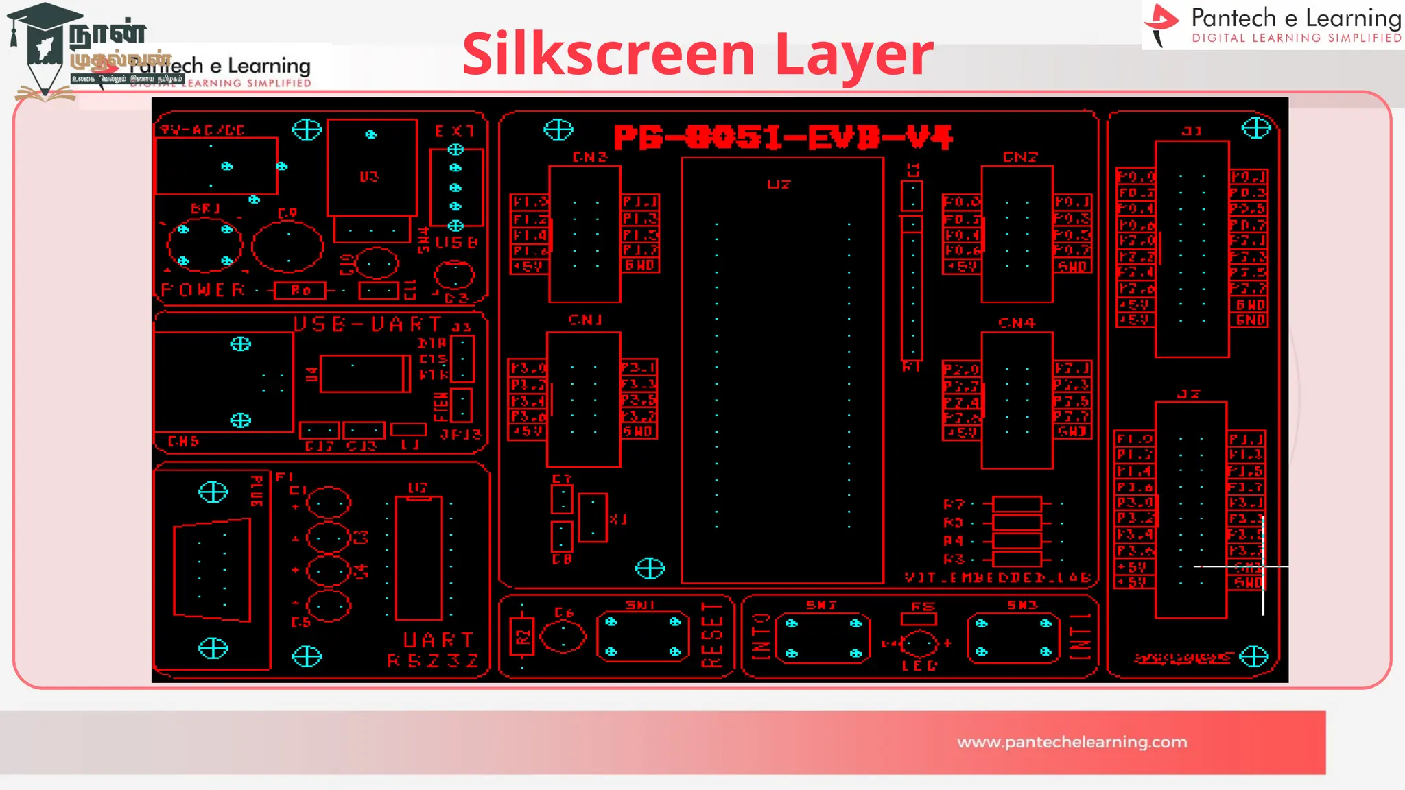
Silkscreen – layer allows the user to use symbols, text, numbers, etc.,
16.
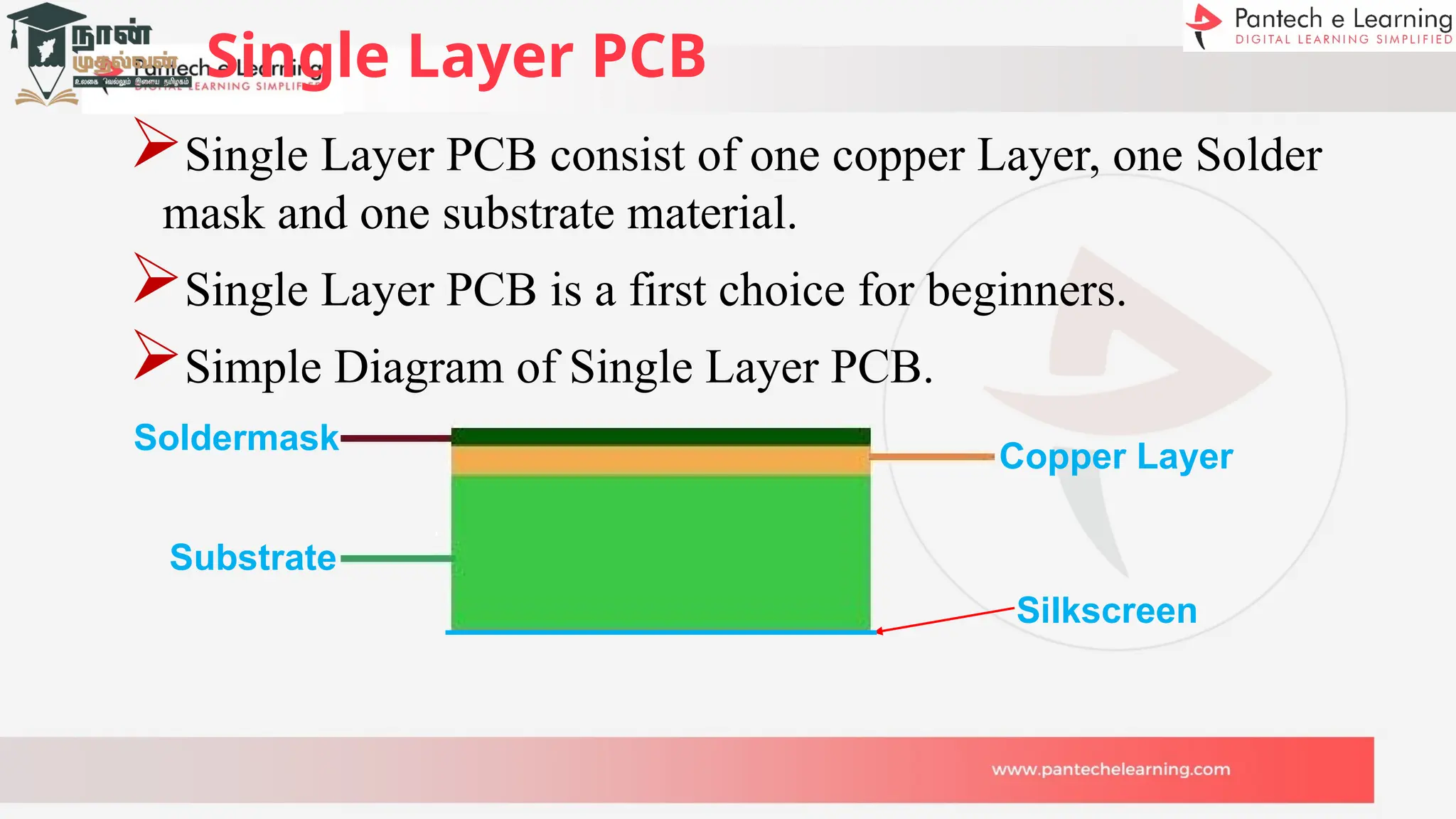
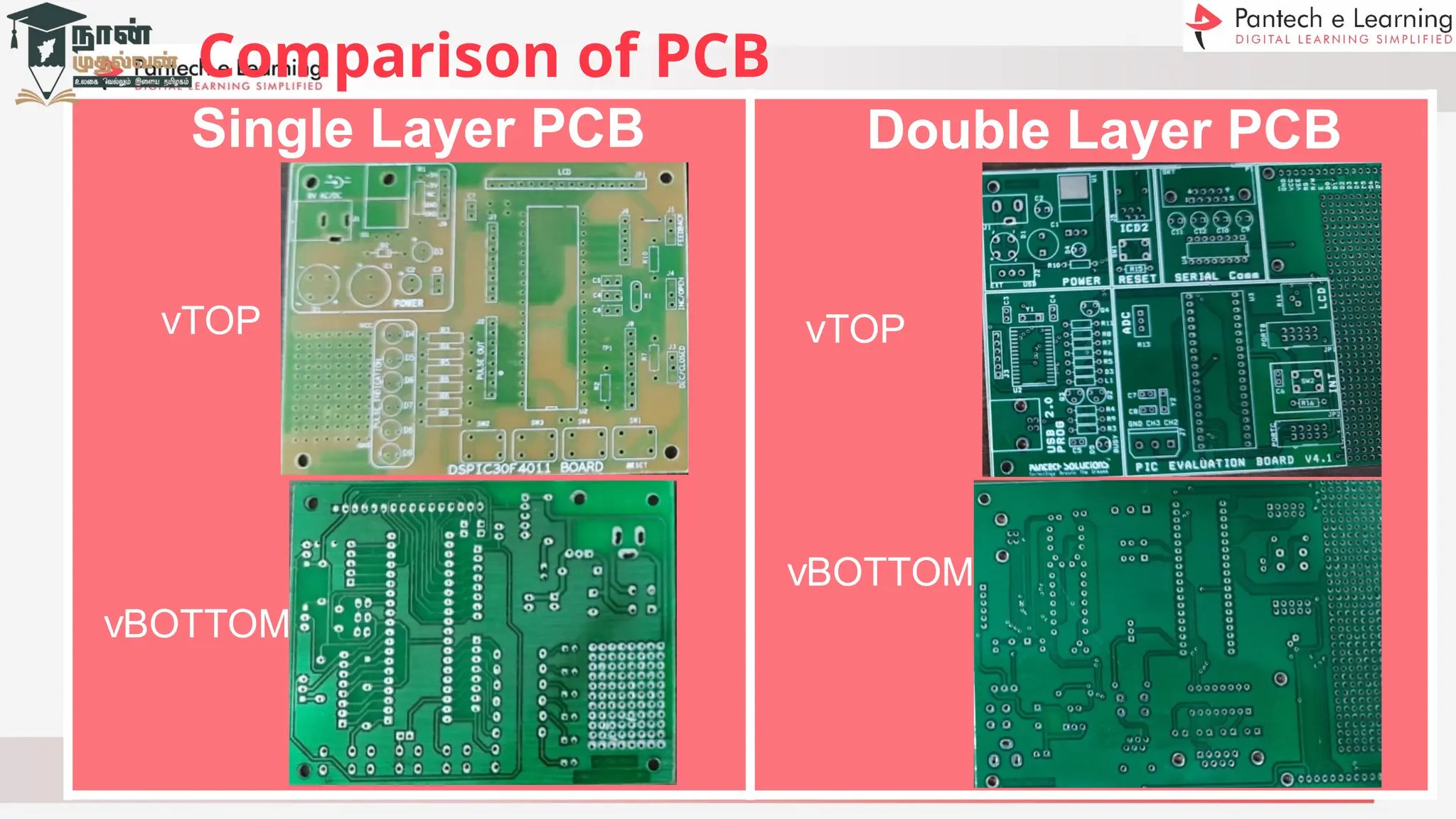
Single Layer PCB
SingleLayer PCB consist of one copper Layer, one Solder
mask and one substrate material.
Single Layer PCB is a first choice for beginners.
Simple Diagram of Single Layer PCB.
Silkscreen
Copper Layer
Substrate
Soldermask
17.
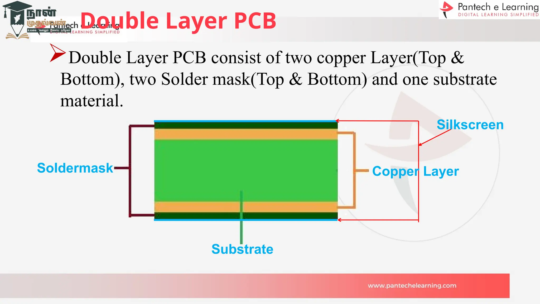
Double Layer PCB
DoubleLayer PCB consist of two copper Layer(Top &
Bottom), two Solder mask(Top & Bottom) and one substrate
material.
Silkscreen
Copper Layer
Substrate
Soldermask
18.
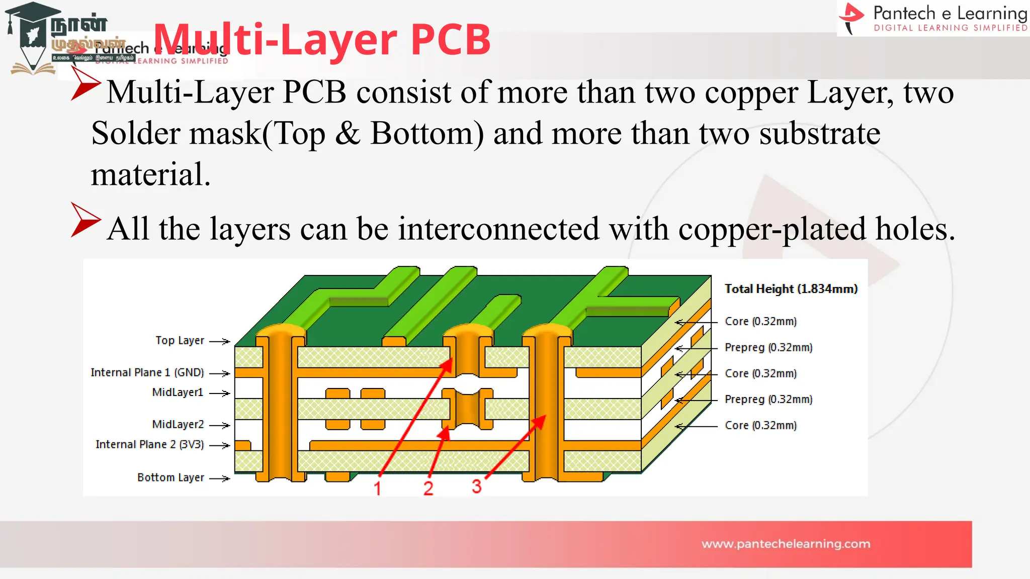
Multi-Layer PCB
Multi-Layer PCBconsist of more than two copper Layer, two
Solder mask(Top & Bottom) and more than two substrate
material.
All the layers can be interconnected with copper-plated holes.
19.
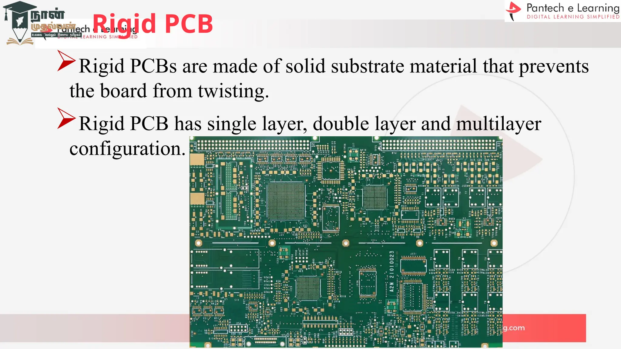
Rigid PCB
Rigid PCBsare made of solid substrate material that prevents
the board from twisting.
Rigid PCB has single layer, double layer and multilayer
configuration.
20.
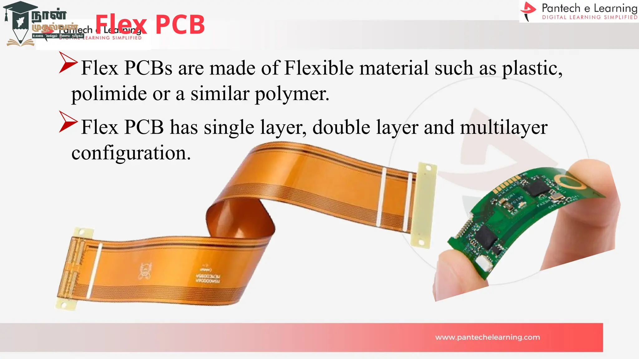
Flex PCB
Flex PCBsare made of Flexible material such as plastic,
polimide or a similar polymer.
Flex PCB has single layer, double layer and multilayer
configuration.
21.
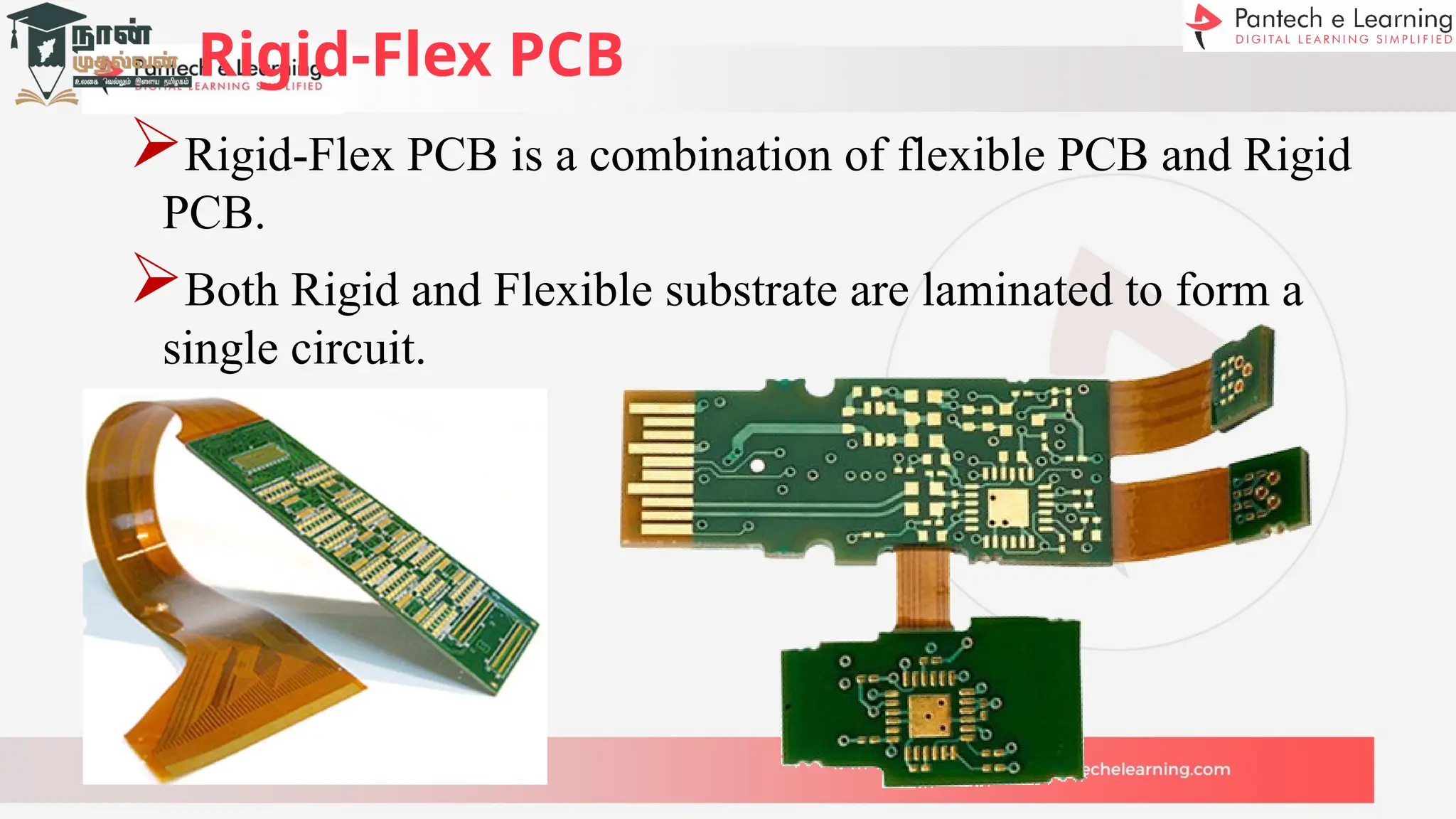
Rigid-Flex PCB
Rigid-Flex PCBis a combination of flexible PCB and Rigid
PCB.
Both Rigid and Flexible substrate are laminated to form a
single circuit.
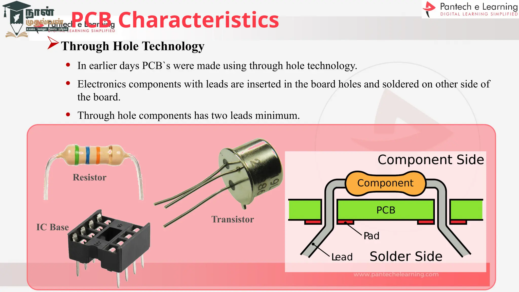
PCB Characteristics
Through HoleTechnology
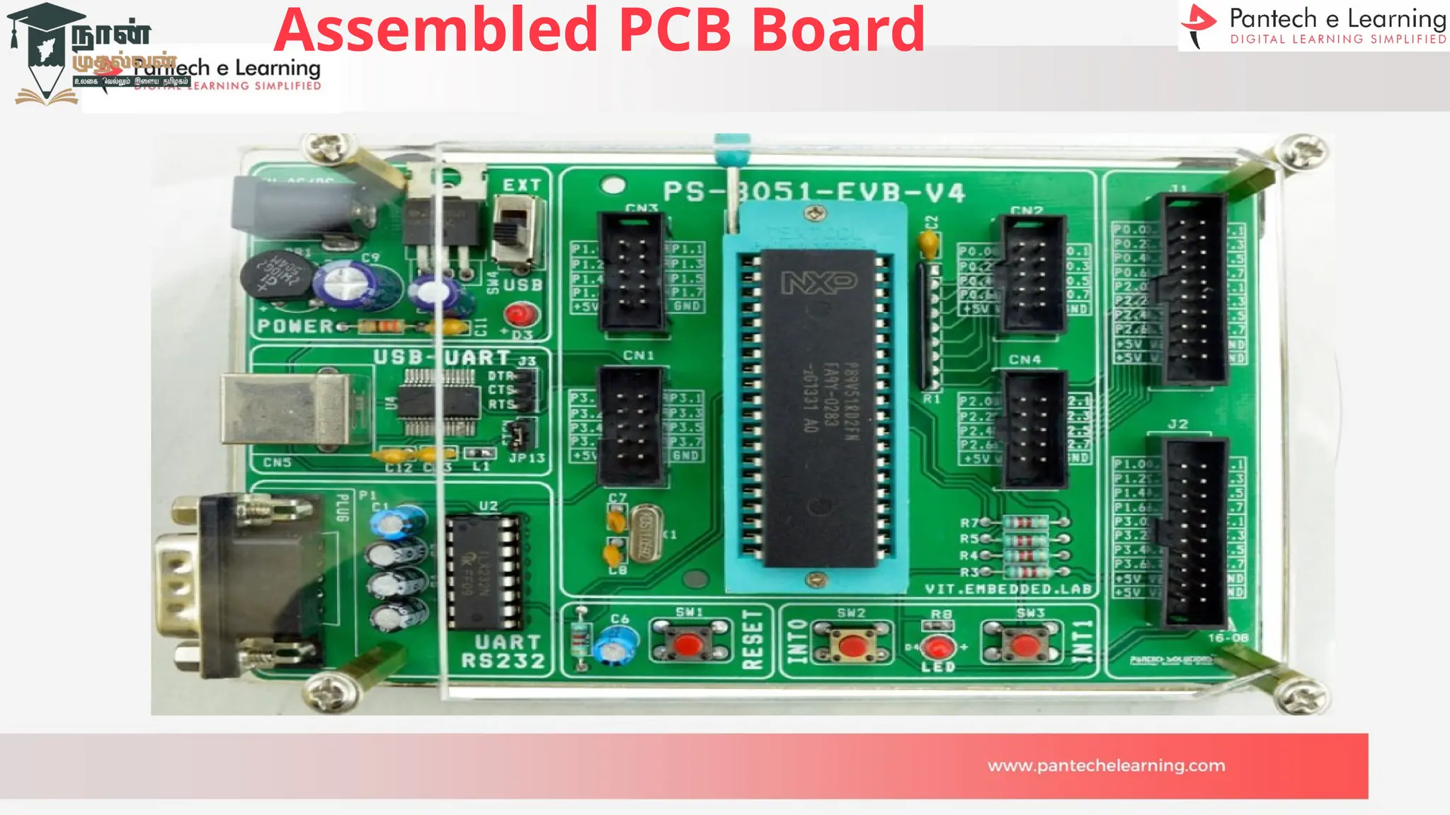
• In earlier days PCB`s were made using through hole technology.
• Electronics components with leads are inserted in the board holes and soldered on other side of
the board.
• Through hole components has two leads minimum.
Resistor
Transistor
IC Base
24.
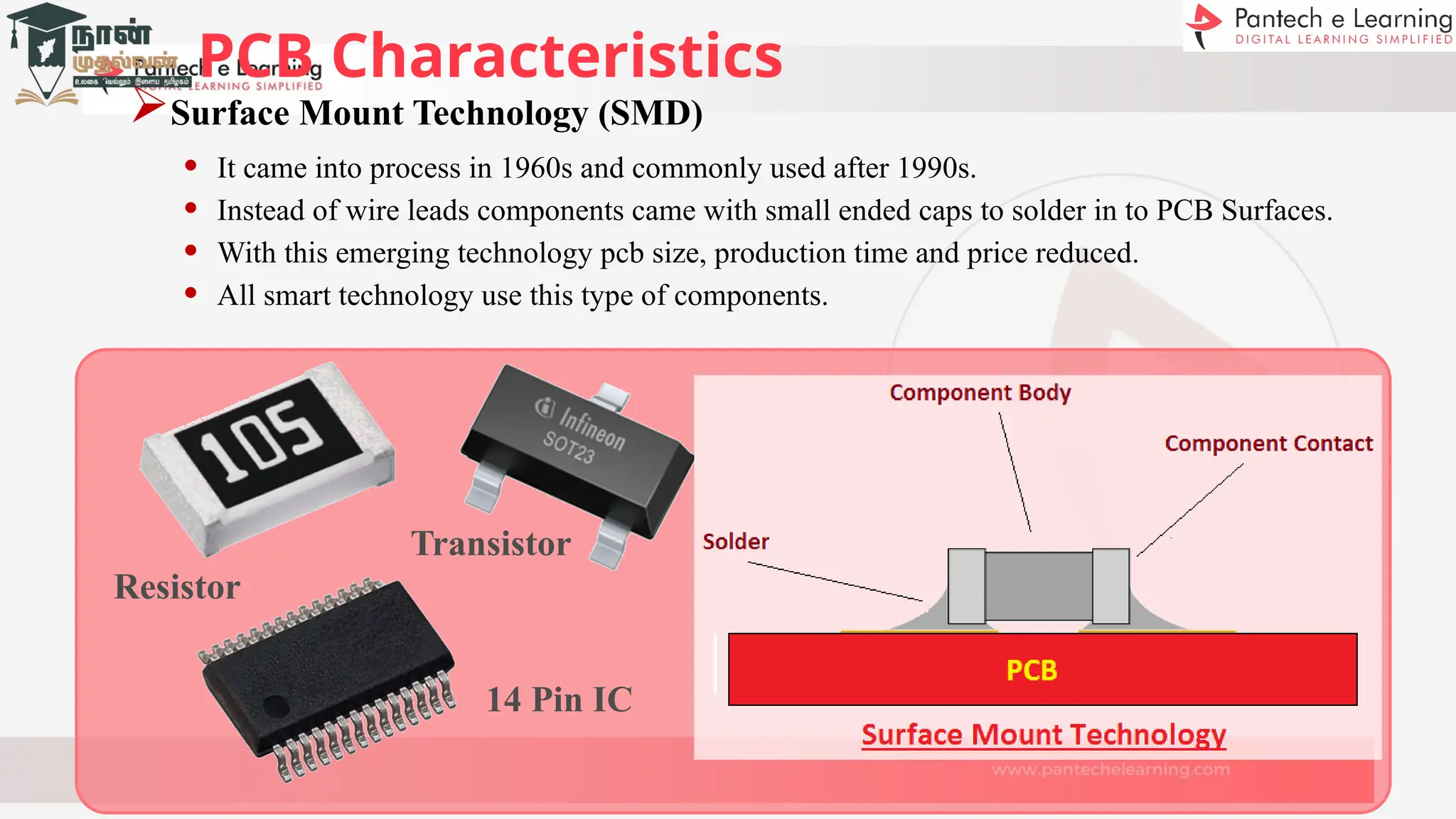
PCB Characteristics
Surface MountTechnology (SMD)
• It came into process in 1960s and commonly used after 1990s.
• Instead of wire leads components came with small ended caps to solder in to PCB Surfaces.
• With this emerging technology pcb size, production time and price reduced.
• All smart technology use this type of components.
Resistor
Transistor
14 Pin IC
25.
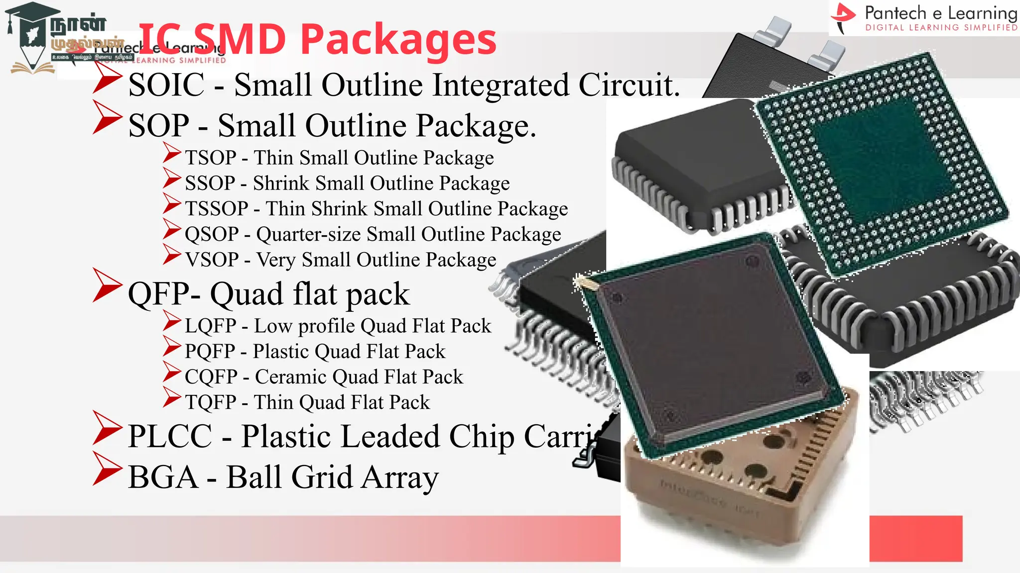
IC SMD Packages
SOIC- Small Outline Integrated Circuit.
SOP - Small Outline Package.
TSOP - Thin Small Outline Package
SSOP - Shrink Small Outline Package
TSSOP - Thin Shrink Small Outline Package
QSOP - Quarter-size Small Outline Package
VSOP - Very Small Outline Package
QFP- Quad flat pack
LQFP - Low profile Quad Flat Pack
PQFP - Plastic Quad Flat Pack
CQFP - Ceramic Quad Flat Pack
TQFP - Thin Quad Flat Pack
PLCC - Plastic Leaded Chip Carrier
BGA - Ball Grid Array
26.
Thinks to know
TestedCircuit Diagram
Choosing components package such as Through hole or SMD
package
Every components Datasheet with pin details and dimension
Choosing appropriate type of PCB, either single layer, double layer,
multilayer etc.,
Current rating going to be handled by PCB
Pre prediction of components placement
Prediction of size and structure of PCB
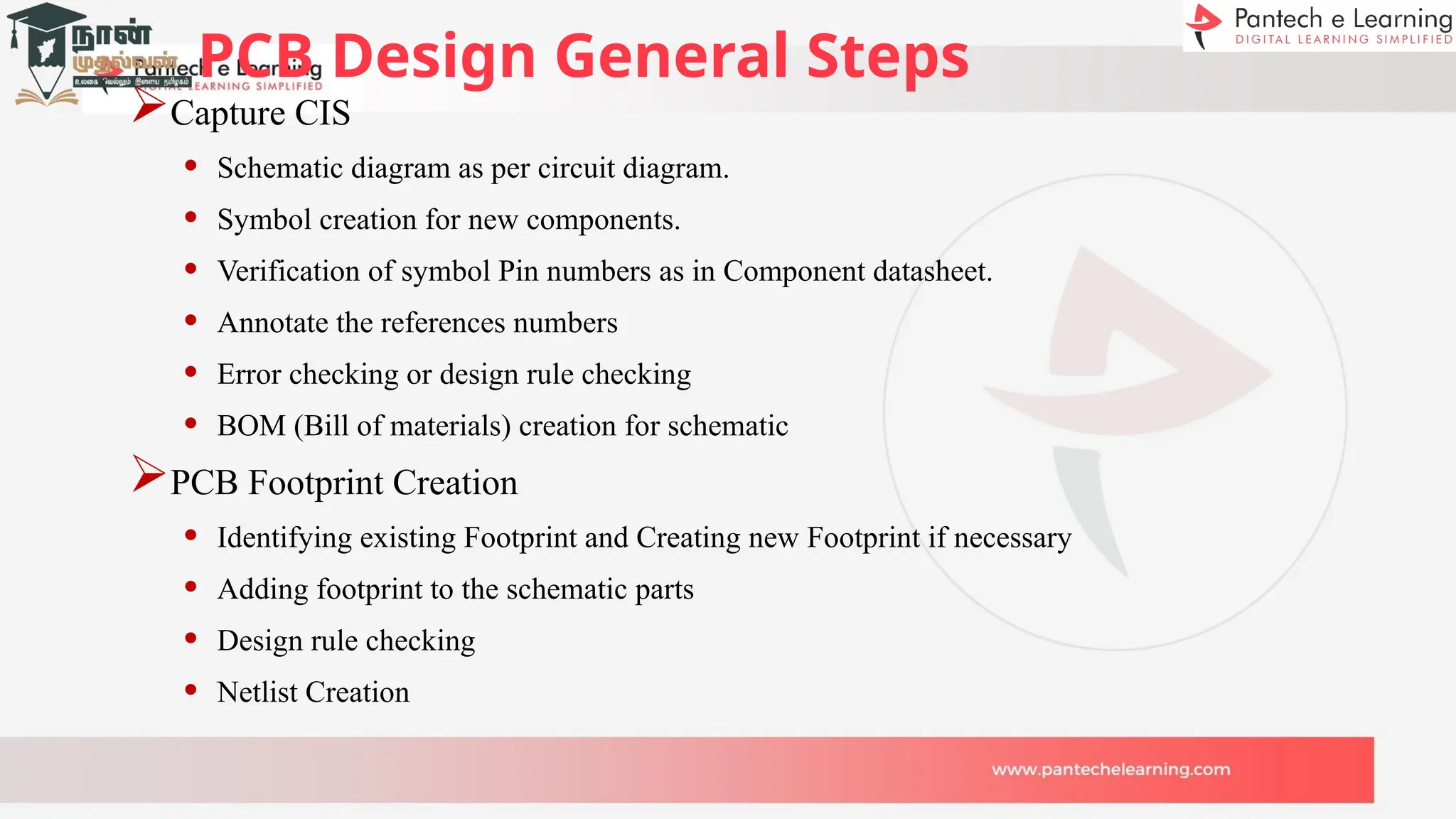
PCB Design GeneralSteps
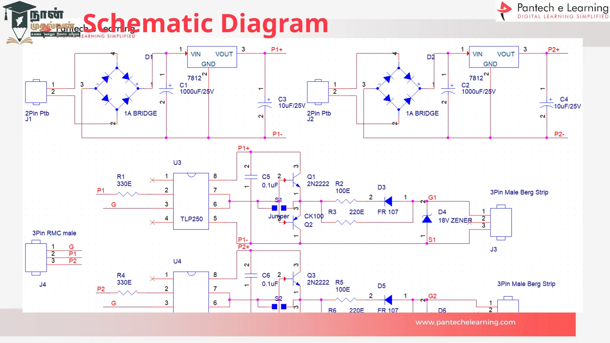
Capture CIS
• Schematic diagram as per circuit diagram.
• Symbol creation for new components.
• Verification of symbol Pin numbers as in Component datasheet.
• Annotate the references numbers
• Error checking or design rule checking
• BOM (Bill of materials) creation for schematic
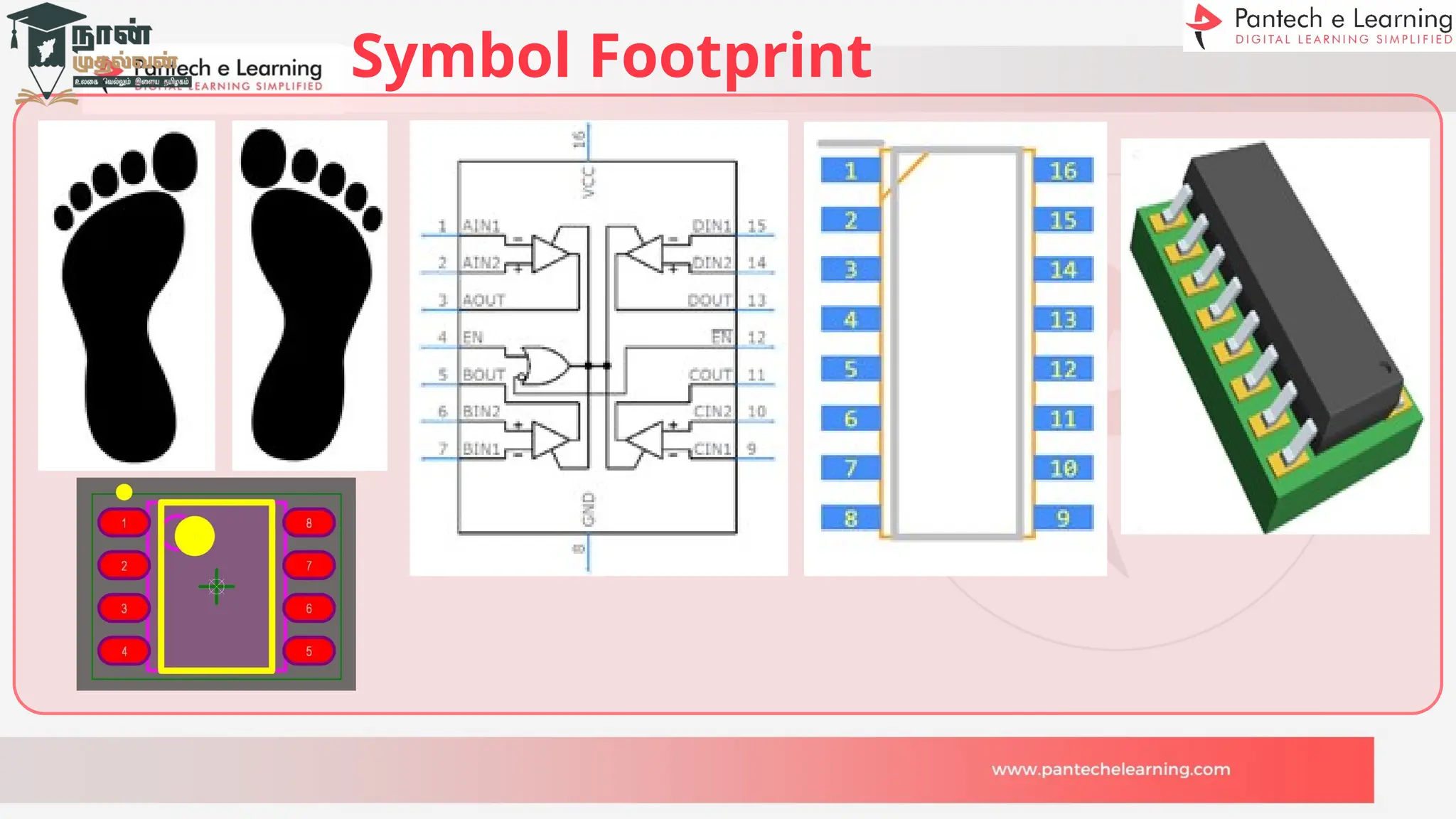
PCB Footprint Creation
• Identifying existing Footprint and Creating new Footprint if necessary
• Adding footprint to the schematic parts
• Design rule checking
• Netlist Creation
29.
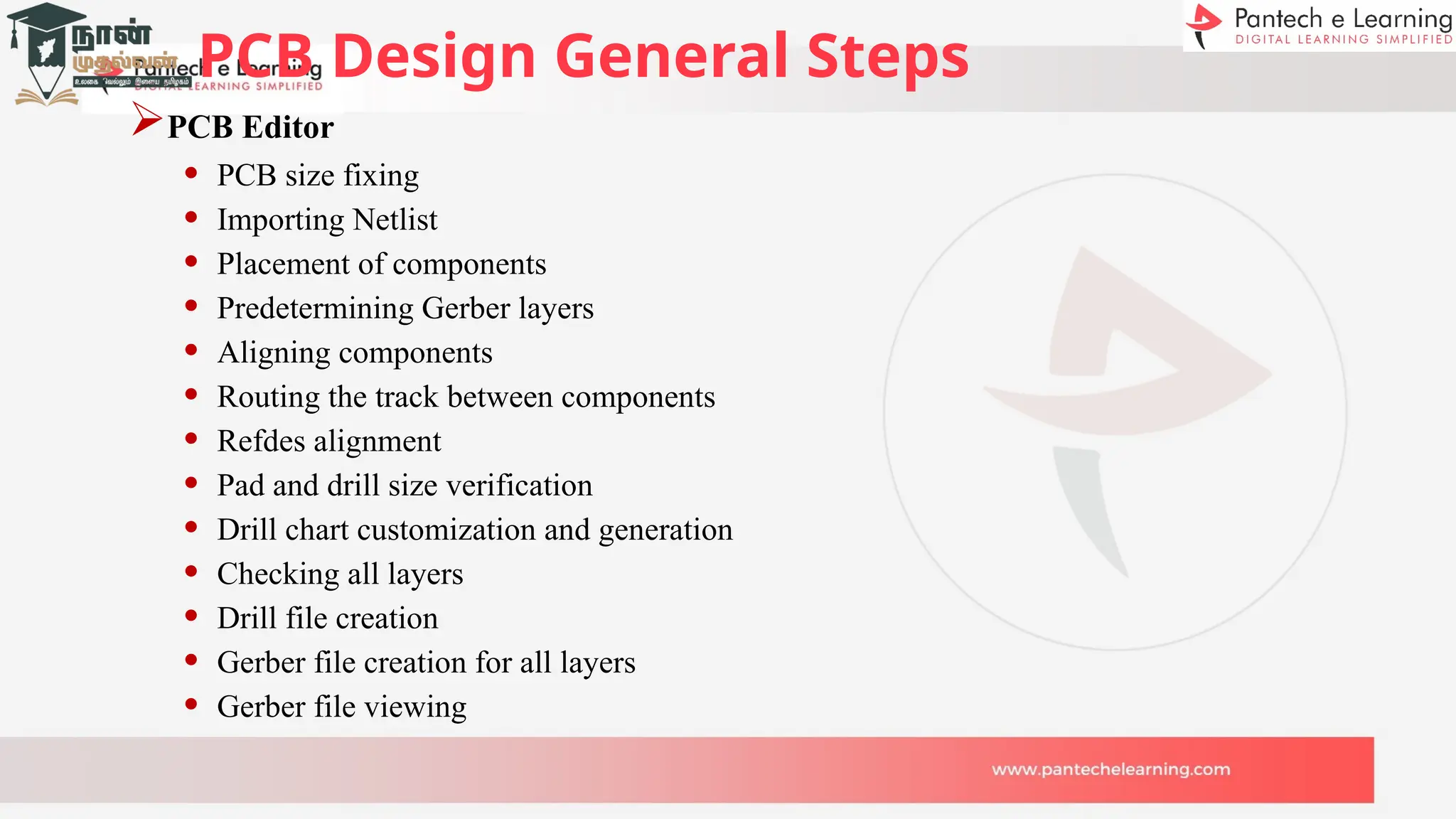
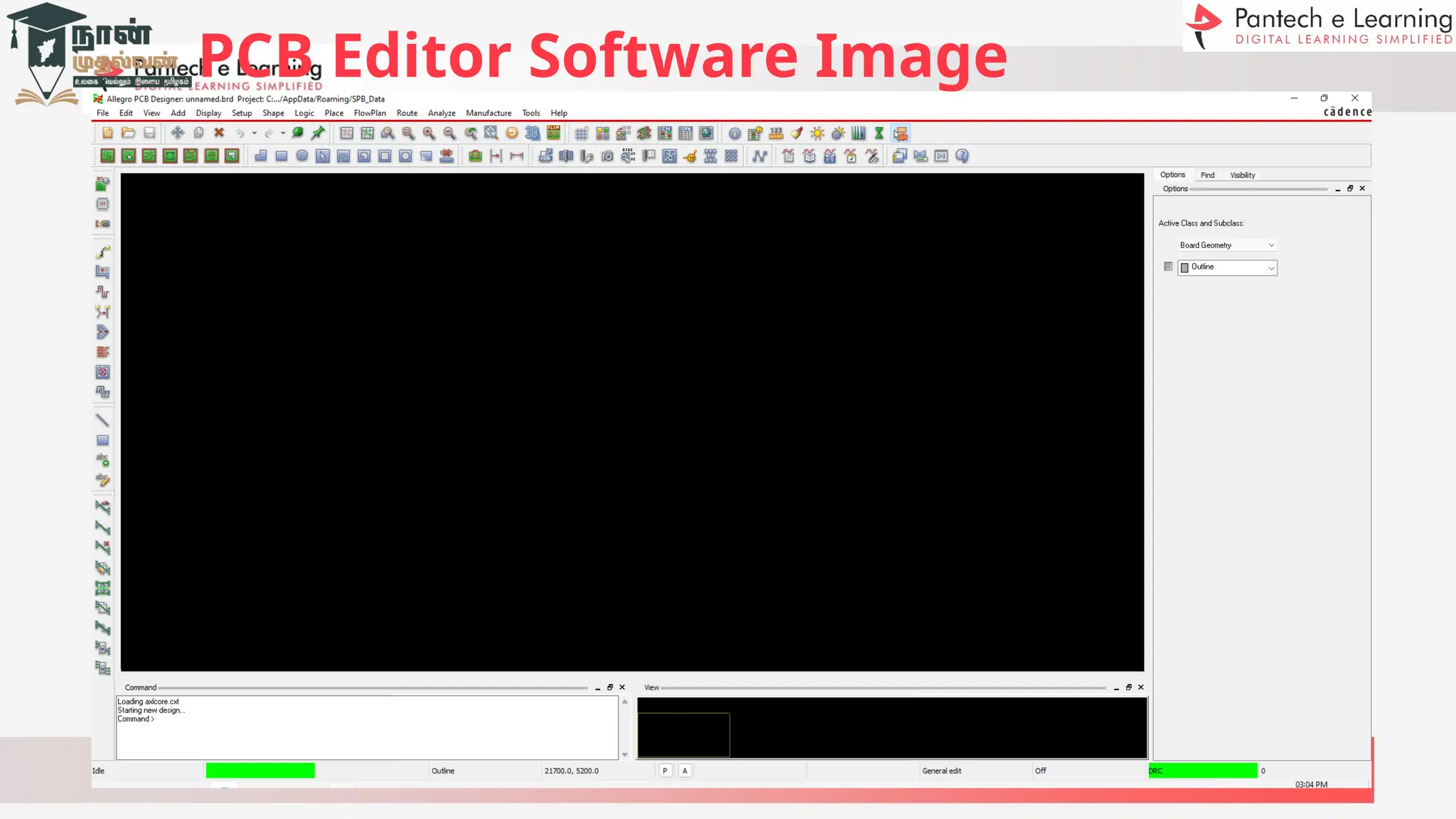
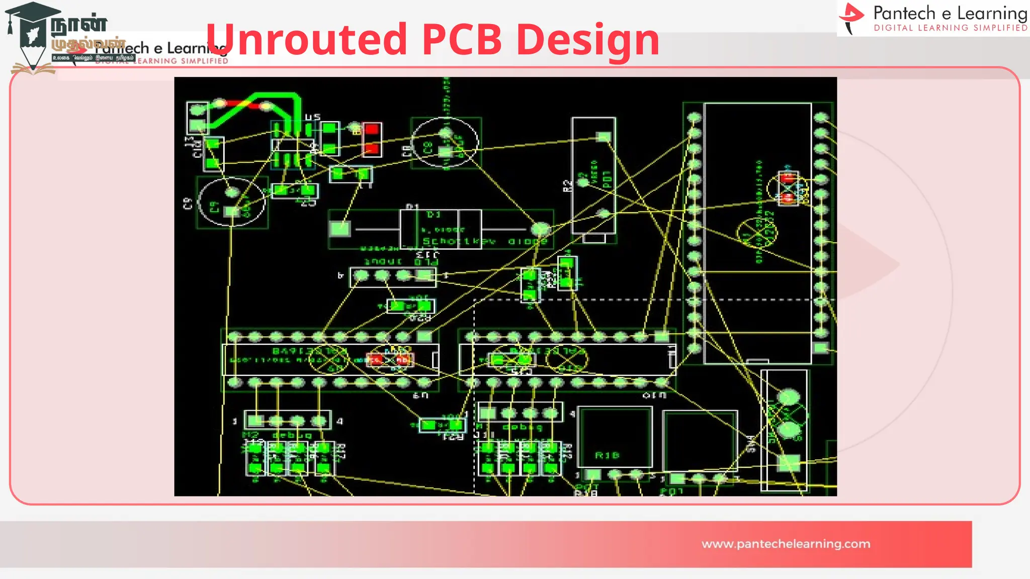
PCB Design GeneralSteps
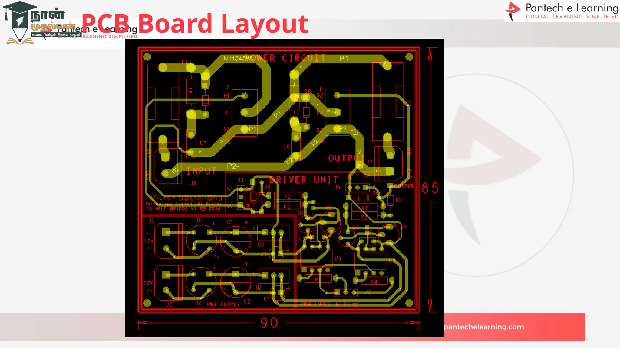
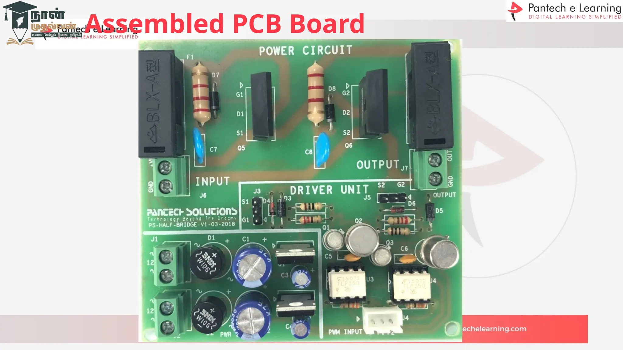
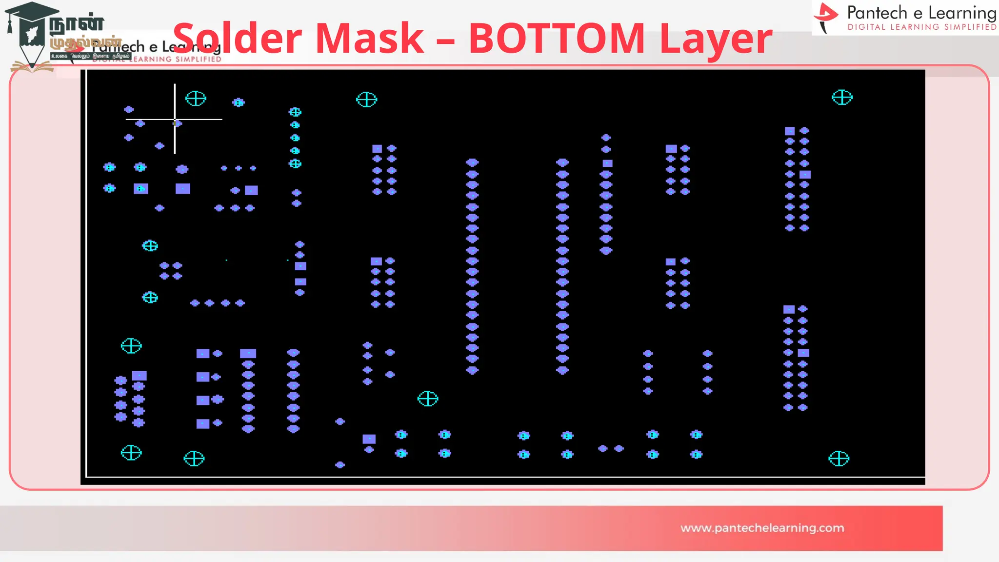
PCB Editor
• PCB size fixing
• Importing Netlist
• Placement of components
• Predetermining Gerber layers
• Aligning components
• Routing the track between components
• Refdes alignment
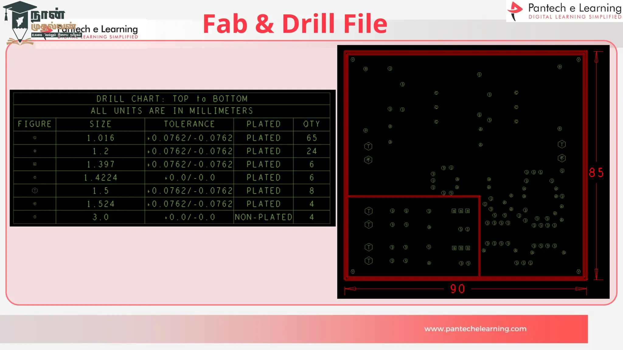
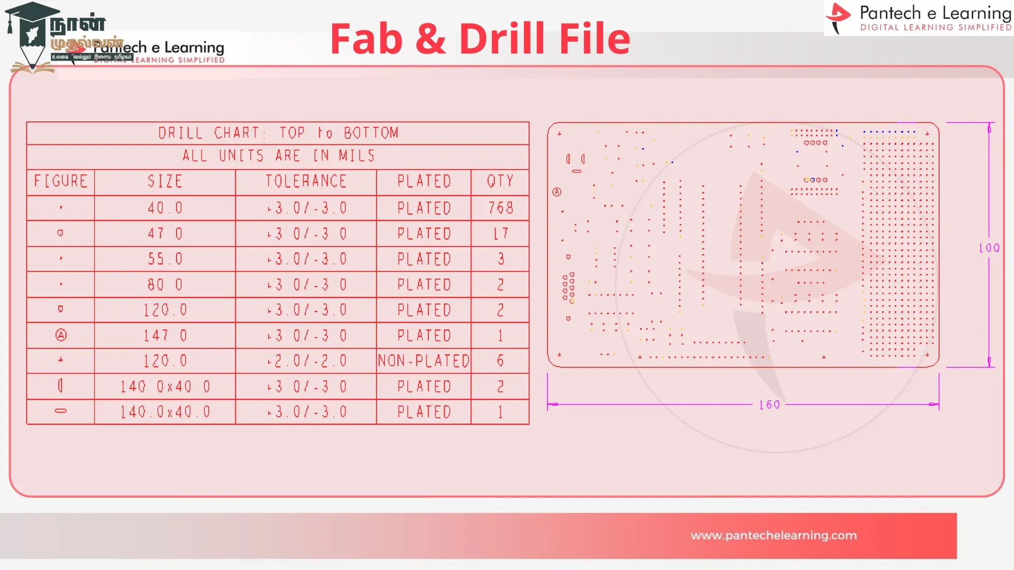
• Pad and drill size verification
• Drill chart customization and generation
• Checking all layers
• Drill file creation
• Gerber file creation for all layers
• Gerber file viewing