Downloaded 189 times

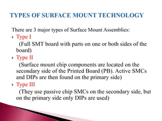
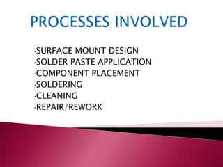

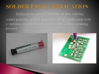
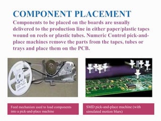

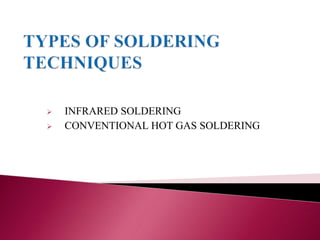

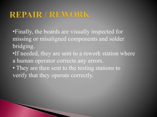
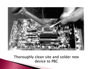


Surface mount technology involves attaching electronic components directly to the surface of printed circuit boards, as opposed to through-hole technology where components are inserted into holes. There are three main types of surface mount assemblies depending on whether components are mounted on one or both sides of the board. The surface mount process involves designing the board, applying solder paste, placing components, soldering, cleaning, and potential repair. Infrared and hot gas soldering are two common soldering techniques used. Reworking involves removing faulty components and soldering new ones in their place.


