Downloaded 221 times


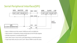
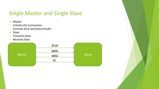
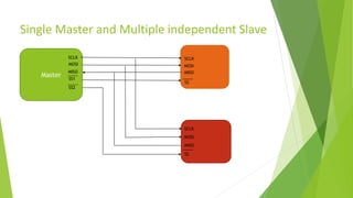

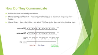


The document provides a comprehensive overview of the Serial Peripheral Interface (SPI), detailing its communication protocol developed by Motorola, which operates on a master-slave configuration and uses four main signal wires for data transfer. It discusses the advantages and disadvantages of SPI, such as full duplex communication and higher throughput compared to I2C but requires more pins and lacks hardware flow control. Additional sections cover the specifics of the SPI control, clock, and data registers, along with practical application information and configurations for both master and slave modes.