

Recommended
More Related Content
What's hot
What's hot (20)
Viewers also liked
Viewers also liked (20)
Similar to Anu Mehra ppt - 2
Similar to Anu Mehra ppt - 2 (20)
Recently uploaded
Recently uploaded (20)
Anu Mehra ppt - 2
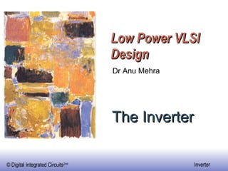
- 1. Low Power VLSI Design The Inverter Dr Anu Mehra
- 2. The CMOS Inverter: A First Glance V in V out C L V DD
- 3. CMOS Inverter Polysilicon In Out GND PMOS 2 Metal 1 NMOS Contacts N Well V DD
- 4. Two Inverters Connect in Metal Share power and ground Abut cells
- 5. CMOS Inverter First-Order DC Analysis V OL = 0 V OH = V DD V M = f(R n , R p ) V DD V DD V in 5 V DD V in 5 0 V out V out R n R p
- 6. CMOS Inverter: Transient Response V out V out R n R p V DD V DD V in 5 V DD V in 5 0 (a) Low-to-high (b) High-to-low C L C L t pHL = f(R on .C L ) = 0.69 R on C L
- 8. PMOS Load Lines V DSp I Dp V GSp =-2.5 V GSp =-1 V DSp I Dn V in =0 V in =1.5 V out I Dn V in =0 V in =1.5 V in = V DD +V GSp I Dn = - I Dp V out = V DD +V DSp V out I Dn V in = V DD +V GSp I Dn = - I Dp V out = V DD +V DSp
- 9. CMOS Inverter Load Characteristics
- 11. Switching Threshold as a function of Transistor Ratio 10 0 10 1 0.8 0.9 1 1.1 1.2 1.3 1.4 1.5 1.6 1.7 1.8 M V (V) W p /W n
- 12. Determining V IH and V IL A simplified approach V OH V OL V in V out V M V IL V IH
- 13. Inverter Gain
- 14. Simulated VTC
- 16. CMOS Inverter Propagation Delay Approach 1 ∆ t=C L ∆V/I DS Iav is average charging current and ∆V is V DD /2 V DD V out V in = V DD C L I av t pHL = C L V swing /2 I av
- 17. CMOS Inverter Propagation Delay Approach 2
- 18. Transient Response t p = 0.69 C L (R eqn +R eqp )/2 t pLH t pHL
- 19. Delay as a function of V DD
- 20. The Transistor as a Switch
- 27. NMOS/PMOS ratio tpLH tpHL tp = W p /W n