CMOS
• Complementary MOS(CMOS) Inverter analysis makes
use of both NMOS and PMOS transistors in the same
logic gate.
• All static parameters of CMOS inverters are superior to
those of NMOS inverters
• Price paid for these substantial improvements
– Increased process complexity to provide isolated
transistors of both polarity types.
3.
CMOS
• CMOS mostwidely used digital circuit technology in
comparison to other logic families.
– lowest power dissipation
– highest packing density
Virtually all modern microprocessors are manufactured
in CMOS and older version are now reprocessed in
CMOS technology.
• Advantage of having both transistors in the same logic
gate comes from the value of VGS
needed to enable the
Drain-Source current channel.
4.
CMOS
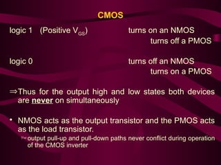
logic 1 (PositiveVGS
) turns on an NMOS
turns off a PMOS
logic 0 turns off an NMOS
turns on a PMOS
ÞThus for the output high and low states both devices
are never on simultaneously
• NMOS acts as the output transistor and the PMOS acts
as the load transistor.
output pull-up and pull-down paths never conflict during operation
of the CMOS inverter
5.
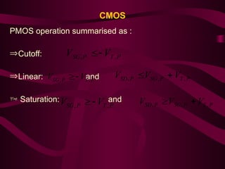
CMOS
PMOS operation summarisedas :
ÞCutoff:
ÞLinear: and
Saturation: and
P
T
P
SG V
V ,
,
P
T
P
SG V
V ,
,
P
T
P
SG
P
SD V
V
V ,
,
,
P
T
P
SG V
V ,
,
P
T
P
SG
P
SD V
V
V ,
,
,
6.
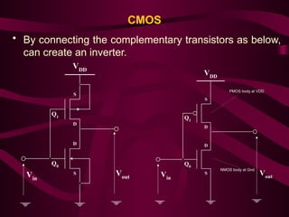
CMOS
• By connectingthe complementary transistors as below,
can create an inverter.
VDD
Vin
Vout
Q0
Q1
D
D
S
S
VDD
Vin
Vout
Q0
Q1
D
D
S
S
PMOS body at VDD
NMOS body at Gnd
7.
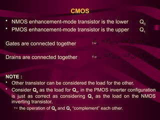
CMOS
• NMOS enhancement-modetransistor is the lower Q0
• PMOS enhancement-mode transistor is the upper Q1
Gates are connected together
Drains are connected together
NOTE :
• Other transistor can be considered the load for the other.
• Consider Q0
as the load for Q1
, in the PMOS inverter configuration
is just as correct as considering Q1
as the load on the NMOS
inverting transistor.
the operation of Q0
and Q1
“complement” each other.
P
SG
DD
N
GS
in V
V
V
V ,
,
P
SD
DD
N
DS
out V
V
V
V ,
,
8.
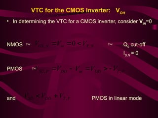
VTC for theCMOS Inverter: VOH
• In determining the VTC for a CMOS inverter, consider VIN
=0
NMOS Q0
cut-off
ID,N
= 0
PMOS
and PMOS in linear mode
N
T
in
N
GS V
V
V ,
, 0
P
T
DD
in
DD
P
SG V
V
V
V
V ,
,
P
T
DD
SD V
V
V ,
9.
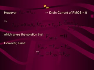
VOH
However DrainCurrent of PMOS = 0
which gives the solution that
However, since
N
D
P
D I
I ,
,
P
SD
P
SD
P
T
P
SG
P
P
D V
V
V
V
I ,
,
,
,
,
2
0
0
,
P
SD
V
out
DD
P
SD V
V
V
,
OH
DD
out V
V
V
10.
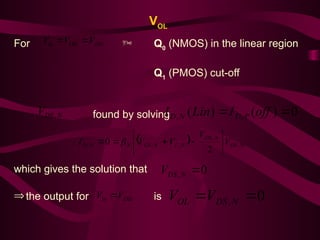
VOL
For Q0
(NMOS)in the linear region
Q1
(PMOS) cut-off
found by solving
which gives the solution that
Þthe output for is
DD
OH
in V
V
V
N
DS
V , 0
)
(
)
( ,
,
off
I
Lin
I P
D
N
D
N
DS
N
DS
N
T
N
GS
N
N
D V
V
V
V
I ,
,
,
,
,
2
0
0
,
N
DS
V
DD
in V
V 0
,
N
DS
OL V
V
11.
VOL
• Unlike theNMOS inverter configurations, the
output of a CMOS inverter does reduce all
the way to 0V.
• Since output can range from 0 volts to VDD
Þ output is said to “rail-to-rail”
12.
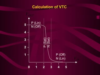
Calculation of VTC
•Find critical points, VOH
, VOL
, VIL
and VIH
.
VIL
NMOS operation in saturation region
PMOS operates in linear mode
– Equate currents to obtain VIL
and corresponding output
voltage.
VIH
NMOS operation in linear region
PMOS operates in saturation mode
– Equate currents to obtain VIH
and corresponding output
voltage.
13.
Calculation of VTC
12 3 4 5
IN
V
0
OUT
V
1
2
3
4
5
P (Off)
N (Lin)
P (Lin)
N (Off)
P
(Sat)
N
(Sat)
14.
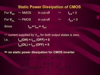
Static Power Dissipationof CMOS
For VOH
NMOS in cut-off ID,N
= 0
For VOL
PMOS in cut-off -ID,P
= 0
Since IDD
= ID,N
= -ID,P
current supplied by VDD for both output states is zero.
i.e. IDD
(OH) = ID,N
(OFF) = 0
IDD
(OL) = ID,P
(OFF) = 0
no static power dissipation for CMOS inverter
DD
DD
DD
DD V
OL
I
OH
I
avg
P
2
)
(
)
(
)
(
0
2
0
0
)
(
DD
DD V
avg
P
15.
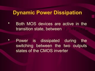
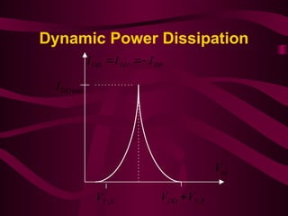
Dynamic Power Dissipation
•Both MOS devices are active in the
transition state, between
• Power is dissipated during the
switching between the two outputs
states of the CMOS inverter
IH
IN
IL V
V
V
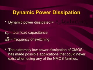
Dynamic Power Dissipation
•Dynamic power dissipated =
CT = total load capacitance
= frequency of switching
• The extremely low power dissipation of CMOS
has made possible applications that could never
exist when using any of the NMOS families.
2
DD
T
DD V
C
dyn
P
18.
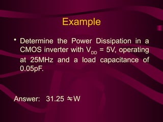
Example
• Determine thePower Dissipation in a
CMOS inverter with VDD
= 5V, operating
at 25MHz and a load capacitance of
0.05pF.
Answer: 31.25 W
19.
Design of SymmetricCMOS
Inverters
• A valuable aspect of CMOS is that a
symmetric VTC is easily obtainable.
• One reason for designing with a symmetric
VTC is to obtain a symmetric transient
response.
20.
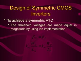
Design of SymmetricCMOS
Inverters
• To achieve a symmetric VTC
• The threshold voltages are made equal in
magnitude by using ion implementation.
P
P
P
N
N
N
P
N
L
W
k
L
W
k '
'
21.
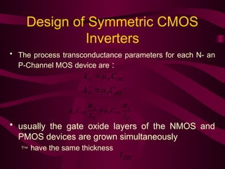
Design of SymmetricCMOS
Inverters
• The process transconductance parameters for each N- an
P-Channel MOS device are :
• usually the gate oxide layers of the NMOS and
PMOS devices are grown simultaneously
have the same thickness
OX
P
P
OX
N
N
C
k
C
k
'
'
P
P
OX
P
N
N
OX
N
L
W
C
L
W
C
OX
t
22.
Design of SymmetricCMOS
Inverters
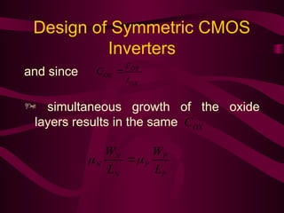
and since
simultaneous growth of the oxide
layers results in the same
OX
OX
OX
t
C
OX
C
P
P
P
N
N
N
L
W
L
W
23.
Design of SymmetricCMOS
Inverters
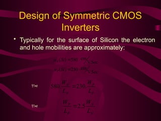
• Typically for the surface of Silicon the electron
and hole mobilities are approximately:
V.Sec
cm
230
)
(
V.Sec
cm
580
)
(
Si
Si
P
N
P
P
N
N
L
W
L
W
.
230
.
580
N
N
P
P
L
W
L
W
5
.
2
24.
Design of SymmetricCMOS
Inverters
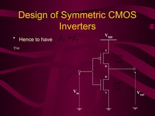
• Hence to have
P
N
VDD
Vin Vout
D
D
S
S
m
m
2
10
m
m
2
4
25.
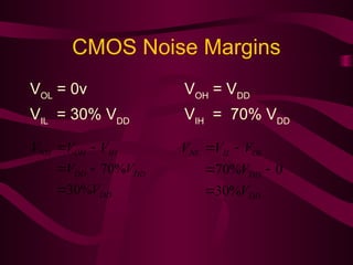
CMOS Noise Margins
VOL
=0v VOH
= VDD
VIL
= 30% VDD
VIH
= 70% VDD
DD
DD
DD
IH
OH
NH
V
V
V
V
V
V
%
30
%
70
DD
DD
OL
IL
NL
V
V
V
V
V
%
30
0
%
70
26.
CMOS Noise Margins
•Noise margins are same in both states and depend
on VDD
.
• At VDD
= 5V noise margins are both 1.5V
• Substantially better than TTL and ECL
• This makes CMOS attractive for applications that
are exposed to high noise environments.
• Noise margins can be made even wider by using a
higher value of VDD
.
– improvement obtained at the expense of a higher drain
on the power because of the higher supply voltage.
27.
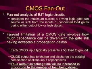
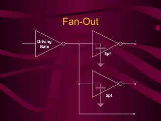
CMOS Fan-Out
• Fan-outanalysis of BJT logic circuits
– considers the maximum current a driving logic gate can
source or sink from the inputs of connected load gates
during either output low or high states.
• Fan-out limitation of a CMOS gate involves how
much capacitance can be driven with the gate still
having acceptable propagation delays
– Each CMOS input typically presents a 5pf load to ground.
ÞCMOS output has to charge and discharge the parallel
combination of all the input capacitances
ÞThus output switching time will be increased in
proportion to the number of load being driven.
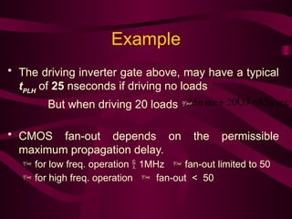
Example
• The drivinginverter gate above, may have a typical
tPLH
of 25 nseconds if driving no loads
But when driving 20 loads
• CMOS fan-out depends on the permissible
maximum propagation delay.
for low freq. operation 1MHz fan-out limited to 50
for high freq. operation fan-out < 50
sec
85
3
20
sec
25 n
n
30.
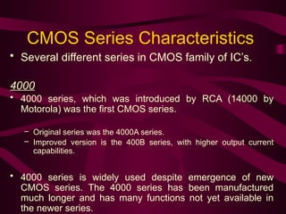
CMOS Series Characteristics
•Several different series in CMOS family of IC’s.
4000
• 4000 series, which was introduced by RCA (14000 by
Motorola) was the first CMOS series.
– Original series was the 4000A series.
– Improved version is the 400B series, with higher output current
capabilities.
• 4000 series is widely used despite emergence of new
CMOS series. The 4000 series has been manufactured
much longer and has many functions not yet available in
the newer series.
31.
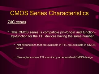
CMOS Series Characteristics
74Cseries
• This CMOS series is compatible pin-for-pin and function-
by-function for the TTL devices having the same number.
– Not all functions that are available in TTL are available in CMOS
series.
– Can replace some TTL circuits by an equivalent CMOS design.
32.
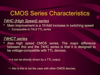
CMOS Series Characteristics
74HC(High Speed) series
• Main improvement is a 10-fold increase in switching speed
– Comparable to 74LS TTL series
74HCT series
• Also high speed CMOS series. The major difference
between this and the 74HC series is that it is designed to
be voltage-compatible with TTL devices.
Þit can be directly driven by a TTL output.
this is this is not the case with other CMOS devices.
33.
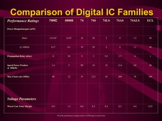
Performance Ratings 74HC4000B 74 74S 74LS 74AS 74ALS ECL
Power Dissipation/gate (mW)
Static 2.5x10⁻³
1x10⁻³
10 20 2 8 1.2 40
@ 100kHz 0.17 0.1 10 20 2 8 1.2 40
Propagation Delay (nSec) 8 50 9 3 9.5 1.7 4 1
Speed Power Product
@ 100kHz
1.4 5 90 10 19 13.6 4.8 40
Max Clock rate (MHz) 40 12 35 12.5 45 200 70 300
Voltage Parameters
Worst Case Noise Margin 0.9 1.5 0.4 0.3 0.3 0.3 0.4 0.25
Comparison of Digital IC Families
All of the performance ratings are for a NAND gate in each series.
34.
Particular Notes onCMOS
• All CMOS inputs on a package (eg. Multi-gate
chip) must be connected to a fixed voltage 0v or
VDD
or another input.
• Applies to even to inputs of extra unused logic
gates on a chip.
–An unconnected CMOS input is susceptible to noise
and static charges that could easily bias both the P
and N channel devices in the conductive state
increased power dissipation & overheating.
35.
Particular Notes onCMOS
• High input resistance of CMOS inputs makes them
especially prone to static-charge build-up that can
produce voltages large enough to break down the
dielectric insulation between the FET’s gate and
channel.
– Most of newer CMOS devices have protected Zener
diodes on each input.
– Diodes are designed to turn-on and limit the size of the
input voltage to well below any damage value.
– While diodes usually function fine, sometimes they do not
turn on quickly enough to prevent the IC from being
damaged
• good practice to use special handling