CMOS inverter
2
The chapterintroduces the CMOS inverter, a fundamental building block for all CMOS logic gates.
Despite its simple structure, the inverter's operation involves complex electronic behavior.
Understanding the CMOS inverter is very important because:
❑ It forms the basis for more complex gates like NAND and NOR gates.
❑ It helps explain the electrical behavior of CMOS digital circuits.
❑ It highlights how small defects can alter inverter performance, leading to CMOS circuit
failures.
3.
CMOS Logic Gatesand Digital Operation
3
CMOS logic gates are categorized as digital cells, which means:
❑ They perform operations based on Boolean algebra.
❑ Both inputs and outputs operate within two distinct logic levels, typically:
• Logic High (1)
• Logic Low (0)
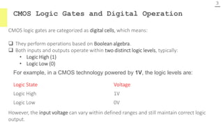
Logic State Voltage
Logic High 1V
Logic Low 0V
For example, in a CMOS technology powered by 1V, the logic levels are:
However, the input voltage can vary within defined ranges and still maintain correct logic
output.
4.
4
Noise Immunity inDigital Circuits
One key advantage of digital circuits like CMOS gates is their noise immunity, meaning:
❑ Small fluctuations or disturbances in input voltage are tolerated if they remain within
allowable logic ranges.
❑ Unlike analog circuits, where small voltage changes can cause significant errors, digital
circuits avoid such problems.
Undefined Voltage Range
In addition to the two defined logic states, there is a third voltage range:
❑ This range exists between the high and low logic levels.
❑ It occurs during transitions when input or output voltages change state.
❑ Under normal, stable (quiescent) operation, no circuit node remains in this undefined
range.
❑ These intermediate voltages carry no valid logic meaning.
5.
THE CMOS INVERTER
5
Functionof an Inverter
An inverter is one of the most basic logic gates. Its job is simple:
•It converts a logic high to a logic low, or
•It converts a logic low to a logic high. Input Voltage
(Vin)
Output Voltage
(Vout)
High (e.g., 1V) Low (0V)
Low (0V) High (e.g., 1V)
The Boolean expression for an inverter is:
Vout= 𝑉𝑖𝑛
6.
CMOS Inverter Structure
6
TheCMOS inverter uses two complementary transistors:
❑ An nMOS transistor, which conducts when the input is high.
❑ A pMOS transistor, which conducts when the input is low.
These two act like complementary switches:
Input Voltage pMOS nMOS Output Behavior
High (e.g., 1V) OFF ON
Output pulled to 0V
(Logic Low)
Low (0V) ON OFF
Output pulled to 1V
(Logic High)
7.
7
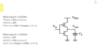
When Input A= 0 (LOW):
•PMOS is ON (conducts)
•NMOS is OFF
•Path from VDD → Output, so Y = 1
When Input A = 1 (HIGH):
•PMOS is OFF
•NMOS is ON (conducts)
•Path from Output → GND, so Y = 0
8.
Steady-State (Quiescent) Behavior
8
Inthe quiescent state, meaning when the circuit is stable and not transitioning:
❑ Only one transistor conducts at a time.
❑ The output is connected to either the power supply (VDD) or ground (GND),
depending on the input.
❑ There is no direct current path between VDD and GND, meaning no steady-state
power consumption.
❑ This makes CMOS inverters highly energy-efficient in steady-state operation.
9.
Load Capacitance (CL)
9
Theoutput node of the inverter connects to some parasitic capacitance, represented as CLCL,
which comes from:
❑ The transistor's internal capacitances.
❑ The wiring or interconnections in the circuit.
While CLCL does not affect static behavior, it plays an important role in dynamic behavior,
specifically:
❑ It slows down logic transitions (switching from high to low or low to high).
❑ The capacitor must charge or discharge during each transition, which takes time.
❑ Larger capacitances lead to slower circuits.
Thus, CLCL directly impacts the speed of digital circuits.
Static and Dynamic Analysis
•Static analysis focuses on behavior when the circuit is stable (steady
output levels).
•Dynamic analysis studies the circuit's behavior during transitions (how
quickly the output switches states).
10.
10
The output parasiticcapacitance CLC (also called load capacitance) plays a critical role
in determining the dynamic performance, particularly the speed and power consumption, of
CMOS digital circuits
Switching Speed (Propagation Delay)
• When a CMOS gate switches output from LOW to HIGH or HIGH to LOW, it must charge
or discharge the load capacitance CLC through the PMOS or NMOS transistors. This
charging and discharging process takes time, resulting in propagation delay.
• Tpd ∝ R⋅CL
Dynamic power consumption occurs each time the output switches from 0 to 1, as energy is
required to charge the load capacitance CLC to the supply voltage VDD, and this power is
mathematically expressed as Pdynamic=α⋅CL⋅VDD2⋅f, where αalphaα is the activity factor,
and f is the switching frequency
11.
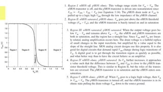
Inverter Static Operation11
Voltage Characteristic. The static voltage characteristic
measures the logic gate input
and output voltage over the whole voltage range. This
curve defines the voltage levels mapped to each logic
state. Figure 4.2 shows an inverter static voltage
transfer curve (Vout versus Vin). Noise margin refers to
the amount of input signal variation allowed before the
output voltage shows a significant change. Noise
margins are often simplistically defined at the points of
the curve where the slope is -1. There are five bias state
regions corresponding to the transistor operating
regions.
13
Region I: nMOSOff, pMOS Ohmic
Vin<Vtn (very low input voltage)
nMOS: Off
pMOS: On (linear/ohmic region)
Output Vout≈VDD
Region II: nMOS Saturated, pMOS Ohmic
•Vin is just above Vtn
•nMOS: On (saturation)
•pMOS: On (ohmic)
•Output starts to drop from high
Region III: Both nMOS and pMOS Saturated
•Middle of the transition (steep slope in the VTC)
•nMOS: Saturation
•pMOS: Saturation
•Linear gain region → Acts like an amplifier (analog
region)
•Very sensitive to input changes
Region IV: nMOS Ohmic, pMOS Saturated
•VinV_{in}Vin increases more
•nMOS: Ohmic
•pMOS: Saturation
•Output goes near ground
Region V: nMOS Ohmic, pMOS Off
•Vin>VDD−Vtp
•nMOS: On (ohmic)
•pMOS: Off
•Output Vout≈ 0 (logic low)
14.
1 0 /0 7 / 2 0 2 5 D i g i t a l I C D e s i g n
14
Except for Region I and Region V, the point at which transistors change from one zone
to another depends on the inverter input and output voltages (Regions I and V depend only
on the input). The input voltage at which these changes occur depends on the relative sizing
of the devices, since the transistor width-to-length dimension (W/L) determines the
current for a given gate–source voltage and, therefore, the effective equivalent resistance
between drain and source.
15.
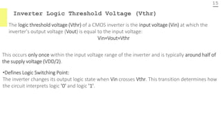
Inverter Logic ThresholdVoltage (Vthr)
15
The logic threshold voltage (Vthr) of a CMOS inverter is the input voltage (Vin) at which the
inverter's output voltage (Vout) is equal to the input voltage:
Vin=Vout=Vthr
This occurs only once within the input voltage range of the inverter and is typically around half of
the supply voltage (VDD/2).
•Defines Logic Switching Point:
The inverter changes its output logic state when Vin crosses Vthr. This transition determines how
the circuit interprets logic '0' and logic '1'.
16.
Why is VTHRimportant?
16
Defines Logic Switching Point:
The inverter changes its output logic state when Vin crosses Vthr. This transition determines how the circuit
interprets logic '0' and logic '1’.
Critical for Defect Analysis:
In CMOS circuits, defects like leakage paths or weak transistors can cause intermediate voltages at certain
nodes. Whether these voltages lead to a logic malfunction depends on:
•The circuit's Vthr value.
•The actual input voltage at the affected node.
Weak Logic Voltages:
Voltages that are:
Slightly lower than a strong logic '1', or Slightly higher than a strong logic '0’, are considered weak logic
voltages.
These weak logic states may still be interpreted correctly by subsequent gates, but they reduce
noise margins and degrade gate driving capability, making the circuit more susceptible to noise
or further malfunction.
17.
Voltage Levels andNoise Margins in CMOS Logic Circuits
17
In real-world circuits, input and output voltage ranges differ due to:
1. Circuit design variations.
2. The presence of electrical noise.
When digital signals pass between logic gates, they can pick up electrical noise (interference,
signal degradation, etc.). To ensure reliable operation, logic levels must be separated enough
to tolerate some noise. Noise margin quantifies this tolerance.
This requires well-defined voltage limits to ensure reliable logic interpretation between gates.
Term Description
VIL
Input Low Voltage: Maximum voltage still recognized as a
logic '0' at a gate input.
VIH
Input High Voltage: Minimum voltage recognized as a logic '1'
at a gate input.
VOL
Output Low Voltage: Maximum voltage output by a gate for a
logic '0' under specified load conditions.
VOH
Output High Voltage: Minimum voltage output by a gate for a
logic '1' under specified load conditions.
18.
18
Noise Margin High(NMH):
NMH=VOH−VIH
It represents how much noise a HIGH signal
can tolerate before it might be
misinterpreted as LOW.
Noise Margin Low (NML):
NML=VIL−VOL
It represents how much noise a LOW signal
can tolerate before it might be
misinterpreted as HIGH.
Example Calculation
Suppose a digital IC has the following specs:
VOH=4.9v
VIH=2.0v
VIL=0.8v
VOL=0.1V
NMH=4.9−2.0=2.9V
NML=0.8−0.1= 0.7V
These margins mean the logic system can
tolerate:
Up to 2.9V of noise on HIGH-level signals,
Up to 0.7V of noise on LOW-level signals
19.
19
The logic thresholdvoltage of a CMOS inverter depends on the aspect ratio of the
transistors:
Wp
Wn
Both pMOS and nMOS transistors typically have equal channel lengths, so the ratio simplifies to:
Design Goal: Achieve a symmetric transfer characteristic, where:
This happens when the pull-up and pull-down networks are balanced.
20.
20
Aspect Ratio forSymmetric Inverter
The expression for achieving symmetry in the inverter's VTC (Voltage Transfer Characteristic) is:
Where:
•μn μp: electron and hole mobilities
•Vtn Vtp: threshold voltages for nMOS and pMOS
•VDD : supply voltage
Practical Design Consideration
•Since μn>μp , electron mobility is higher.
•Designers often set:
21.
example 21
Given Parameters
•μn=360cm2/V⋅s
•μp=109 cm2
•Vtn=0.35 V
•Vtp=−0.36 V
•VDD=1.8 V
1. Compute mobility ratio
2Compute threshold voltage terms
22.
NAND GATES
22
MOS technologynaturally implements inverting (negated) logic functions.
Common examples:
•Inverter (NOT gate): outputs the complement of the input.
•NAND gate: outputs NOT (A AND B).
•NOR gate: outputs NOT (A OR B).
Noncontrolling Input States
•A noncontrolling input is one that does not
affect the output under certain conditions.
•In a NAND gate:
• Logic 1 is the noncontrolling input.
Dominating Zero Logic
•Any input at logic 0 → Output is 1
•Reason: A⋅B=0 if either A or B is 0 → NAND of
0 is 1
Example:
•If A = 1 → output only depends on B:
• If B = 1 → output = 0
• If B = 0 → output = 1
→ So, C = NOT(B) when A = 1
23.
23
PMOS Transistors (Top– Pull-up Network):
•PMOS transistors conduct when input is LOW (0).
•The PMOS transistors are connected in parallel, so only
one needs to be ON to pull the output HIGH
NMOS Transistors (Bottom – Pull-down
Network):
•NMOS transistors conduct when input is HIGH
(1).
•The NMOS transistors are connected in series, so
both must be ON to pull the output LOW.
Operation by Input Case:
•A = 0, B = 0:
• Both PMOS are ON → Output = HIGH
• Both NMOS are OFF → No path to GND
•A = 0, B = 1 or A = 1, B = 0:
• One PMOS is ON → Output = HIGH
• One NMOS is OFF → No complete path to
GND
•A = 1, B = 1:
• Both PMOS are OFF
• Both NMOS are ON → Output = LOW
(connected to GND)