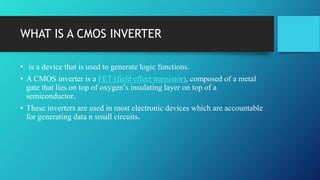
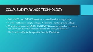
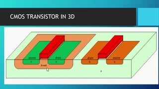
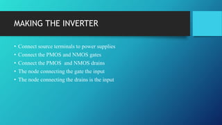
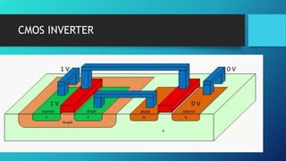
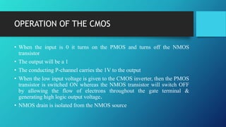
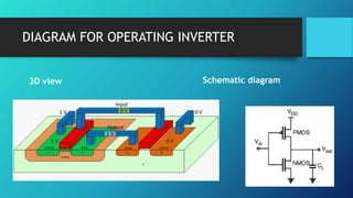
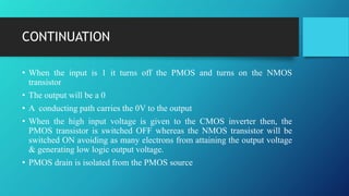
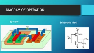
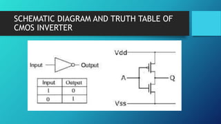
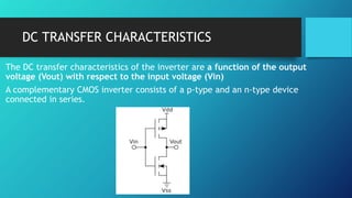
GROUP 1
• ADAMS ANDY PANASHE R195260E
• BASVI VICTOR MUNASHE R195324Z
• BUME TITOS MAPURANGA R197144Q
• CHAPFUWA ADOLF R195300C
• CHIFAMBA ANOTIDA COURAGE R1810988
• CHIGWEREWE ALEX R197132Z
• CHIMUGUNDE TATENDA TENDAI R1813907
CMOS TECHNOLOGY
CMOS INVERTER
WHAT IS A CMOS INVERTER
• is a device that is used to generate logic functions.
• A CMOS inverter is a FET (field effect transistor), composed of a metal
gate that lies on top of oxygen’s insulating layer on top of a
semiconductor.
• These inverters are used in most electronic devices which are accountable
for generating data n small circuits.
COMPLEMENTARY MOS TECHNOLOGY
• Both NMOS and PMOS Transistors are combined on a single chip
• N-well : held power supply voltage, P-substrate : held at ground voltage
• PN region between the NMOS AND PMOS is reverse biased so no current
flows between those PN junctions besides the voltage difference.
• The N-well is effectively separated from the P substrate
CMOS TRANSISTOR IN 3D
MAKING THE INVERTER
• Connect source terminals to power supplies
• Connect the PMOS and NMOS gates
• Connect the PMOS and NMOS drains
• The node connecting the gate the input
• The node connecting the drains is the input
CMOS INVERTER
OPERATION OF THE CMOS
• When the input is 0 it turns on the PMOS and turns off the NMOS
transistor
• The output will be a 1
• The conducting P-channel carries the 1V to the output
• When the low input voltage is given to the CMOS inverter, then the PMOS
transistor is switched ON whereas the NMOS transistor will switch OFF
by allowing the flow of electrons throughout the gate terminal &
generating high logic output voltage.
• NMOS drain is isolated from the NMOS source
DIAGRAM FOR OPERATING INVERTER
3D view Schematic diagram
CONTINUATION
• When the input is 1 it turns off the PMOS and turns on the NMOS
transistor
• The output will be a 0
• A conducting path carries the 0V to the output
• When the high input voltage is given to the CMOS inverter then, the
PMOS transistor is switched OFF whereas the NMOS transistor will be
switched ON avoiding as many electrons from attaining the output voltage
& generating low logic output voltage.
• PMOS drain is isolated from the PMOS source
DIAGRAM OF OPERATION
3D view Schematic view
LAYOUT OF THE CMOS INVERTER
EXPLANATION
• This is the view looking down onto the surface of the CMOS.
• Each transistor is shown in different colour
• NMOS source terminal are connected to 0V
• PMOS source terminal are connected to 1V
• X boxes are for the contacts
• PMOS must be made larger because it is intrinsically weaker than NMOS
and it needs to balance the electrical properties to the NMOS
SCHEMATIC DIAGRAM AND TRUTH TABLE OF
CMOS INVERTER
ADVANTAGES AND DISADVANTAGES
ADVANTAGES
• These are low-cost to produce
mass.
• High noise immunity
• These inverters use electricity
once they are switched ON & OFF
resulting in less power
consumption
DISADVANTAGES
• As compared to other inverters,
the switching speed of the CMOS
inverter is high.
• It uses two transistors to make an
inverter, so it uses more space on
the IC as compared to the NMOS
inverter.
DC TRANSFER CHARACTERISTICS
The DC transfer characteristics of the inverter are a function of the output
voltage (Vout) with respect to the input voltage (Vin)
A complementary CMOS inverter consists of a p-type and an n-type device
connected in series.
DC TRANSFER CHARACTERISTICS
(Graphical analysis)
DC TRANSFER CHARACTERISTICS
(Graphical analysis)
The red dots indicate points of intersections of transfer curves of the
pMOS and the nMOS at the same input
DC TRANSFER CHARACTERISTICS
(Graphical analysis)
Vin Vout
0 0
1 4.9
2 4.4
3 0.6
4 0.1
5 0
OPERATING REGIONS
Threshold Voltage (Vtn) for nMos should be positive and the threshold
Voltage (Vtp) for pMos is negative.
OPERATING REGIONS

HETT406 GROUP 1 PRESENTATION_CMOS inverter.pptx

  • 1.
    GROUP 1 • ADAMSANDY PANASHE R195260E • BASVI VICTOR MUNASHE R195324Z • BUME TITOS MAPURANGA R197144Q • CHAPFUWA ADOLF R195300C • CHIFAMBA ANOTIDA COURAGE R1810988 • CHIGWEREWE ALEX R197132Z • CHIMUGUNDE TATENDA TENDAI R1813907
  • 2.
  • 3.
    WHAT IS ACMOS INVERTER • is a device that is used to generate logic functions. • A CMOS inverter is a FET (field effect transistor), composed of a metal gate that lies on top of oxygen’s insulating layer on top of a semiconductor. • These inverters are used in most electronic devices which are accountable for generating data n small circuits.
  • 4.
    COMPLEMENTARY MOS TECHNOLOGY •Both NMOS and PMOS Transistors are combined on a single chip • N-well : held power supply voltage, P-substrate : held at ground voltage • PN region between the NMOS AND PMOS is reverse biased so no current flows between those PN junctions besides the voltage difference. • The N-well is effectively separated from the P substrate
  • 5.
  • 6.
    MAKING THE INVERTER •Connect source terminals to power supplies • Connect the PMOS and NMOS gates • Connect the PMOS and NMOS drains • The node connecting the gate the input • The node connecting the drains is the input
  • 7.
  • 8.
    OPERATION OF THECMOS • When the input is 0 it turns on the PMOS and turns off the NMOS transistor • The output will be a 1 • The conducting P-channel carries the 1V to the output • When the low input voltage is given to the CMOS inverter, then the PMOS transistor is switched ON whereas the NMOS transistor will switch OFF by allowing the flow of electrons throughout the gate terminal & generating high logic output voltage. • NMOS drain is isolated from the NMOS source
  • 9.
    DIAGRAM FOR OPERATINGINVERTER 3D view Schematic diagram
  • 10.
    CONTINUATION • When theinput is 1 it turns off the PMOS and turns on the NMOS transistor • The output will be a 0 • A conducting path carries the 0V to the output • When the high input voltage is given to the CMOS inverter then, the PMOS transistor is switched OFF whereas the NMOS transistor will be switched ON avoiding as many electrons from attaining the output voltage & generating low logic output voltage. • PMOS drain is isolated from the PMOS source
  • 11.
    DIAGRAM OF OPERATION 3Dview Schematic view
  • 12.
    LAYOUT OF THECMOS INVERTER
  • 13.
    EXPLANATION • This isthe view looking down onto the surface of the CMOS. • Each transistor is shown in different colour • NMOS source terminal are connected to 0V • PMOS source terminal are connected to 1V • X boxes are for the contacts • PMOS must be made larger because it is intrinsically weaker than NMOS and it needs to balance the electrical properties to the NMOS
  • 14.
    SCHEMATIC DIAGRAM ANDTRUTH TABLE OF CMOS INVERTER
  • 15.
    ADVANTAGES AND DISADVANTAGES ADVANTAGES •These are low-cost to produce mass. • High noise immunity • These inverters use electricity once they are switched ON & OFF resulting in less power consumption DISADVANTAGES • As compared to other inverters, the switching speed of the CMOS inverter is high. • It uses two transistors to make an inverter, so it uses more space on the IC as compared to the NMOS inverter.
  • 16.
    DC TRANSFER CHARACTERISTICS TheDC transfer characteristics of the inverter are a function of the output voltage (Vout) with respect to the input voltage (Vin) A complementary CMOS inverter consists of a p-type and an n-type device connected in series.
  • 17.
  • 18.
    DC TRANSFER CHARACTERISTICS (Graphicalanalysis) The red dots indicate points of intersections of transfer curves of the pMOS and the nMOS at the same input
  • 19.
    DC TRANSFER CHARACTERISTICS (Graphicalanalysis) Vin Vout 0 0 1 4.9 2 4.4 3 0.6 4 0.1 5 0
  • 20.
    OPERATING REGIONS Threshold Voltage(Vtn) for nMos should be positive and the threshold Voltage (Vtp) for pMos is negative.
  • 21.