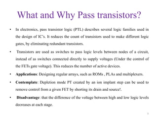
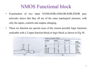
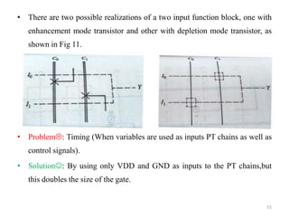
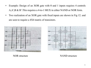
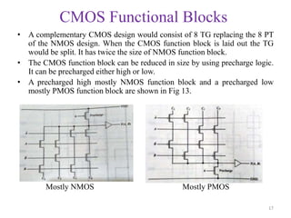
Pass-transistor logic uses transistors as switches to pass logic levels between circuit nodes, rather than connecting directly to power supplies, reducing the number of active devices. It has advantages over standard NMOS gate logic like being minimum geometry and dissipating no standby power. However, voltage differences decrease between logic levels at each stage.
General functional blocks can implement all 16 logic functions of two inputs using NMOS or CMOS pass transistors controlled by four input signals. NMOS blocks pull down to ground but only up to a threshold below power, while CMOS transmission gates can output strong ones and zeros. Precharge logic can reduce the size of CMOS blocks.
This presentation discusses the basics of Pass Transistor Logic, its advantages, limitation and finally implementation of Boolean functions/Combinational Logic circuits using Pass Transistor Logic.
This document discusses the basics of pass transistor logic. It also discusses how to realize ta a boolean equation using PTL , advantages and limitations of pass transistor circuits
A transmission gate is similar to a relay that can conduct in both directions or block by a control signal with almost any voltage potential. CMOS transmission gate consists of one nMOS and one pMOS transistor, connected in parallel. The gate voltages applied to these two transistors are also set to be complementary signals. As such, the CMOS TG operates as a bidirectional switch between the nodes A and B which is controlled by signal C
Multi carrier equalization by restoration of redundanc y (merry) for adaptive...IJNSA Journal
This paper proposes a new blind adaptive channel shortening approach for multi-carrier systems. The
performance of the discrete Fourier transform-DMT (DFT-DMT) system is investigated with the proposed
DST-DMT system over the standard carrier serving area (CSA) loop1. Enhanced bit rates demonstrated
and less complexity also involved by the simulation of the DST-DMT system.
In this paper a review of the dynamic logic circuit design has been done as these circuits are used due to their high performance, high speed and less number of transistors in the circuit. The number of required transistors is lesser than the CMOS logic style. The OR dynamic logic style is not applicable as it has low noise tolerance at the dynamic stage which can change the output. Domino logic uses one static CMOS inverter at the output of dynamic node which is more noise immune and has less capacitance at the output node.
This presentation has given a brief introduction and working of CMOS Logic Structures which includes MOS logic, CMOS logic, CMOS logic structure, CMOS complementary logic, pass transistor logic, bi CMOS logic, pseudo –nMOS logic, CMOS domino logic, Cascode Voltage Switch Logic(CVSL), clocked CMOS logic(c²mos), dynamic CMOS logic
Dee 6113 CMOS IC DESIGN (Chapter 3 ~ CMOS inverter)MielWitwicky
Question 4
a) Draw a schematic diagram of an inverter.
b) Voltage Transfer Characteristics (VTC) is a plot of output voltage as a function of the input voltage. Draw and label the VTC of a CMOS inverter.
c) The inverter is really the nucleus of all digital design. Once its operation and properties are clearly understood, designing more intricate structures such as NAND gates, address, multipliers, and microprocessors is greatly simplified. Therefore, interpret the properties of static CMOS inverter circuit.
Performance Analysis of Encoder in Different Logic Techniques for High-Speed ...Achintya Kumar
In designing a system, we can replace cell components by appropriate technique based cell so that the noise margin of overall circuit is improved. In future we can also implement some techniques for sequential circuits.
This presentation discusses the basics about how to realize logic functions using Static CMOS logic. This presentation discusses about how to realize a Boolean expression by drawing a Pull-up network and a pull-down network. It also briefs about the pass transistor logic and the concepts of weak and strong outputs.
pull up to pull down ratio of nmos inverter driven by another nmos inverter and also another describing with pass transistor. Transistor sizing with example and some formulas
كشف اسماء السيدات المقبولات في الوظائف الصحيةAbdo Magdi
كشف اسماء السيدات المقبولات في الوظائف الصحية
http://www.thaqfny.com/167788/%d8%a7%d9%84%d9%88%d8%b8%d8%a7%d8%a6%d9%81-%d8%a7%d9%84%d8%b5%d8%ad%d9%8a%d8%a9/
What happens when we feel unwelcome? What happens when we do? Find out how, sometimes, we don't welcome differences and cause "ouch" moments. Find out also how to respond in more welcoming ways.
Os presento una descripción el un tema de actualidad, tal como es el Bullying, al igual que sus estrategias,causas para terminar con una campaña de sensibilización de este tema tan espinoso para la adolescencia.
The outcome of the Academy Award for Best Picture surprised us all. But, could that have been predicted? In this practical workshop you'll use a dataset that contains previous Oscar winners to build a prediction model to guess the winner for Best Picture. You'll get an introduction to a data scientist's tools and methods, including an overview of basic machine learning concepts. Unlike this year's Oscars, our model will predict only one winner!
it covers topics Introduction
Classification of Logic Families
Important point
Level of Integration
Specification of Digital ICs
TTL Circuit
TTL NAND Gates
MOS/CMOS Circuits
CMOS NAND Gate
ECL Circuit
Comparison
Numbers of Digital ICs
2011 Protection of a 3.3V Domain and Switchable 1.8V/3.3V I/O in 40nm and 28n...Sofics
2011 Japan RCJ symposium
Today’s advanced technologies’ overdrive transistors cannot always meet the signal speeds of existing standards. This paper describes the issues, solutions and results to build the necessary protection for HBM, MM, CDM and latch-up for a 3.3V domain and 1.8V/3.3V I/O, based only on 1.8V transistors, in a 40nm process. Results of the design ported to 28nm are also presented.
Analysis and Design of A Low-Voltage Low-Power Double-Tail Comparator. This is a final semester Mtech project on VLSI design implementation of dual tail comparator in a modifyied version. This design is implemented using VHDL Language with 100% Source code synthesizable available. Software for free to download and knowledge transfer for the same project is also being implemented..The design is implemented using FSM technology, low power is achieved in this project.area utilization is the major advantage in this project.Low power techniques such as Clock gating, power gating is implemented in this project.,ieee reference paper is used for the base.
PHP Frameworks: I want to break free (IPC Berlin 2024)Ralf Eggert
In this presentation, we examine the challenges and limitations of relying too heavily on PHP frameworks in web development. We discuss the history of PHP and its frameworks to understand how this dependence has evolved. The focus will be on providing concrete tips and strategies to reduce reliance on these frameworks, based on real-world examples and practical considerations. The goal is to equip developers with the skills and knowledge to create more flexible and future-proof web applications. We'll explore the importance of maintaining autonomy in a rapidly changing tech landscape and how to make informed decisions in PHP development.
This talk is aimed at encouraging a more independent approach to using PHP frameworks, moving towards a more flexible and future-proof approach to PHP development.
Generative AI Deep Dive: Advancing from Proof of Concept to ProductionAggregage
Join Maher Hanafi, VP of Engineering at Betterworks, in this new session where he'll share a practical framework to transform Gen AI prototypes into impactful products! He'll delve into the complexities of data collection and management, model selection and optimization, and ensuring security, scalability, and responsible use.
Observability Concepts EVERY Developer Should Know -- DeveloperWeek Europe.pdfPaige Cruz
Monitoring and observability aren’t traditionally found in software curriculums and many of us cobble this knowledge together from whatever vendor or ecosystem we were first introduced to and whatever is a part of your current company’s observability stack.
While the dev and ops silo continues to crumble….many organizations still relegate monitoring & observability as the purview of ops, infra and SRE teams. This is a mistake - achieving a highly observable system requires collaboration up and down the stack.
I, a former op, would like to extend an invitation to all application developers to join the observability party will share these foundational concepts to build on:
DevOps and Testing slides at DASA ConnectKari Kakkonen
My and Rik Marselis slides at 30.5.2024 DASA Connect conference. We discuss about what is testing, then what is agile testing and finally what is Testing in DevOps. Finally we had lovely workshop with the participants trying to find out different ways to think about quality and testing in different parts of the DevOps infinity loop.
LF Energy Webinar: Electrical Grid Modelling and Simulation Through PowSyBl -...DanBrown980551
Do you want to learn how to model and simulate an electrical network from scratch in under an hour?
Then welcome to this PowSyBl workshop, hosted by Rte, the French Transmission System Operator (TSO)!
During the webinar, you will discover the PowSyBl ecosystem as well as handle and study an electrical network through an interactive Python notebook.
PowSyBl is an open source project hosted by LF Energy, which offers a comprehensive set of features for electrical grid modelling and simulation. Among other advanced features, PowSyBl provides:
- A fully editable and extendable library for grid component modelling;
- Visualization tools to display your network;
- Grid simulation tools, such as power flows, security analyses (with or without remedial actions) and sensitivity analyses;
The framework is mostly written in Java, with a Python binding so that Python developers can access PowSyBl functionalities as well.
What you will learn during the webinar:
- For beginners: discover PowSyBl's functionalities through a quick general presentation and the notebook, without needing any expert coding skills;
- For advanced developers: master the skills to efficiently apply PowSyBl functionalities to your real-world scenarios.
Key Trends Shaping the Future of Infrastructure.pdfCheryl Hung
Keynote at DIGIT West Expo, Glasgow on 29 May 2024.
Cheryl Hung, ochery.com
Sr Director, Infrastructure Ecosystem, Arm.
The key trends across hardware, cloud and open-source; exploring how these areas are likely to mature and develop over the short and long-term, and then considering how organisations can position themselves to adapt and thrive.
Dev Dives: Train smarter, not harder – active learning and UiPath LLMs for do...UiPathCommunity
💥 Speed, accuracy, and scaling – discover the superpowers of GenAI in action with UiPath Document Understanding and Communications Mining™:
See how to accelerate model training and optimize model performance with active learning
Learn about the latest enhancements to out-of-the-box document processing – with little to no training required
Get an exclusive demo of the new family of UiPath LLMs – GenAI models specialized for processing different types of documents and messages
This is a hands-on session specifically designed for automation developers and AI enthusiasts seeking to enhance their knowledge in leveraging the latest intelligent document processing capabilities offered by UiPath.
Speakers:
👨🏫 Andras Palfi, Senior Product Manager, UiPath
👩🏫 Lenka Dulovicova, Product Program Manager, UiPath
Epistemic Interaction - tuning interfaces to provide information for AI supportAlan Dix
Paper presented at SYNERGY workshop at AVI 2024, Genoa, Italy. 3rd June 2024
https://alandix.com/academic/papers/synergy2024-epistemic/
As machine learning integrates deeper into human-computer interactions, the concept of epistemic interaction emerges, aiming to refine these interactions to enhance system adaptability. This approach encourages minor, intentional adjustments in user behaviour to enrich the data available for system learning. This paper introduces epistemic interaction within the context of human-system communication, illustrating how deliberate interaction design can improve system understanding and adaptation. Through concrete examples, we demonstrate the potential of epistemic interaction to significantly advance human-computer interaction by leveraging intuitive human communication strategies to inform system design and functionality, offering a novel pathway for enriching user-system engagements.
Essentials of Automations: Optimizing FME Workflows with ParametersSafe Software
Are you looking to streamline your workflows and boost your projects’ efficiency? Do you find yourself searching for ways to add flexibility and control over your FME workflows? If so, you’re in the right place.
Join us for an insightful dive into the world of FME parameters, a critical element in optimizing workflow efficiency. This webinar marks the beginning of our three-part “Essentials of Automation” series. This first webinar is designed to equip you with the knowledge and skills to utilize parameters effectively: enhancing the flexibility, maintainability, and user control of your FME projects.
Here’s what you’ll gain:
- Essentials of FME Parameters: Understand the pivotal role of parameters, including Reader/Writer, Transformer, User, and FME Flow categories. Discover how they are the key to unlocking automation and optimization within your workflows.
- Practical Applications in FME Form: Delve into key user parameter types including choice, connections, and file URLs. Allow users to control how a workflow runs, making your workflows more reusable. Learn to import values and deliver the best user experience for your workflows while enhancing accuracy.
- Optimization Strategies in FME Flow: Explore the creation and strategic deployment of parameters in FME Flow, including the use of deployment and geometry parameters, to maximize workflow efficiency.
- Pro Tips for Success: Gain insights on parameterizing connections and leveraging new features like Conditional Visibility for clarity and simplicity.
We’ll wrap up with a glimpse into future webinars, followed by a Q&A session to address your specific questions surrounding this topic.
Don’t miss this opportunity to elevate your FME expertise and drive your projects to new heights of efficiency.
UiPath Test Automation using UiPath Test Suite series, part 3DianaGray10
Welcome to UiPath Test Automation using UiPath Test Suite series part 3. In this session, we will cover desktop automation along with UI automation.
Topics covered:
UI automation Introduction,
UI automation Sample
Desktop automation flow
Pradeep Chinnala, Senior Consultant Automation Developer @WonderBotz and UiPath MVP
Deepak Rai, Automation Practice Lead, Boundaryless Group and UiPath MVP
A tale of scale & speed: How the US Navy is enabling software delivery from l...sonjaschweigert1
Rapid and secure feature delivery is a goal across every application team and every branch of the DoD. The Navy’s DevSecOps platform, Party Barge, has achieved:
- Reduction in onboarding time from 5 weeks to 1 day
- Improved developer experience and productivity through actionable findings and reduction of false positives
- Maintenance of superior security standards and inherent policy enforcement with Authorization to Operate (ATO)
Development teams can ship efficiently and ensure applications are cyber ready for Navy Authorizing Officials (AOs). In this webinar, Sigma Defense and Anchore will give attendees a look behind the scenes and demo secure pipeline automation and security artifacts that speed up application ATO and time to production.
We will cover:
- How to remove silos in DevSecOps
- How to build efficient development pipeline roles and component templates
- How to deliver security artifacts that matter for ATO’s (SBOMs, vulnerability reports, and policy evidence)
- How to streamline operations with automated policy checks on container images
Accelerate your Kubernetes clusters with Varnish CachingThijs Feryn
A presentation about the usage and availability of Varnish on Kubernetes. This talk explores the capabilities of Varnish caching and shows how to use the Varnish Helm chart to deploy it to Kubernetes.
This presentation was delivered at K8SUG Singapore. See https://feryn.eu/presentations/accelerate-your-kubernetes-clusters-with-varnish-caching-k8sug-singapore-28-2024 for more details.
2. Outline
1. What and Why Pass transistors?
2. Designing Pass transistor logic
3. General Function Blocks
I. NMOS Function Blocks
II. CMOS Function Blocks
2
3. What and Why Pass transistors?
• In electronics, pass transistor logic (PTL) describes several logic families used in
the design of IC’s. It reduces the count of transistors used to make different logic
gates, by eliminating redundant transistors.
• Transistors are used as switches to pass logic levels between nodes of a circuit,
instead of as switches connected directly to supply voltages (Under the control of
the FETs gate voltage). This reduces the number of active devices.
• Applications: Designing regular arrays, such as ROMs , PLAs and multiplexers.
• Contemplate: Depletion mode PT created by an ion implant step can be used to
remove control from a given FET by shorting its drain and source!.
• Disadvantage: that the difference of the voltage between high and low logic levels
decreases at each stage.
3
4. • Two major advantages of PT over standard NMOS gate logic are:
1. They are not “ratiod” devices and can be minimum geometry.
2. They do not have a path from plus supply to ground, and do not
dissipate standby power.
• If the gate and drain of a pass transistor are both high, the source will rise
to the lower of the potentials VDD and VGS – VTH.
• If the gate and drain are both at VDD , the source can only rise to one
threshold voltage below the gate, as shown in Fig 1.
4
5. • Consider the Fig 2.
• Three pass transistor driving an inverter.
• With gate and drain of the first pass transistor at 5V its source rises to 3.5V
and the device is at the onset of pinching off.
• With the gate bias of the second FET at 5V and its drain at 3.5V, its source
rises to the drain potential 3.5V, and the device passes the input voltage to
its output (Depletion mode devices are short circuited).
• Each additional input requires only a minimum-geometry FET and adds no
DC power dissipation to the circuit.
5
6. • Disadvantages: Chare steering, For Fig 2. inputs A,B,C and D all at 5V.
The voltage presented to inverter input is only 3.5V. This must be sufficient
to drive the inverter output low.
• If a PT is driven by a voltage less than 5V, the source of that FET will be at
one threshold voltage less than corresponding gate voltage.
• Fig 3. shows a situation when input C is 3.5V, Which would be the case if it
were driven by a pass transistor. Even though input D is 5V, the voltage to
the inverter is only 2V. This is below inverter threshold voltage and is most
likely treated as logic 0.
• A sufficiently high inverter ratio will solve this problem, but at the expense
of a long pull-up.
6
7. • Thumb Rule: In designing NMOS PT logic, one must never drive a PT
with the output of another PT!
• Another one: In designing PT logic, care must be taken to ensure the
existence of both charging and discharging paths to the inputs of all
inverters!
• Charge sharing is a serious problem which occurs when two or more
capacitors at different potentials are tied together. One must be aware of
sneak paths.
• Sneak path is created when two PT are both on at the same time and one is
connected to VDD while the other is connected to GND, as shown in Fig 4.
7
8. • There is also a timing problem!
• One more rule : One must always provide both a charging and a
discharging path for all input variables!
• A PT chain driving a capacitive load is shown in Fig 5.
• PT can be approximated as a lumped RC equivalent circuit. Where C is
gate to channel capacitance plus any parasitic capacitance of the gate node.
R is the series resistance of the channel with the FET operating in the linear
region, plus any parasitic resistance between nodes .
8
9. • The rise time is proportional to the total resistance Rt and the total
capacitance Ct, of the line, both of which double when the number of PT
doubles. Hence propagation time is proportional to the square of the
number of PT in the chain.
• A string (finite transmission) of N elements, a string of identical pass
transistor driving a matched load CL=Cg, exhibits a delay of approximately
tp = 0.7N(N+1) RCL/2
• More accurate estimate for the propagation delay times low to high tpLH,
and high to low tpHL are
tpLH = 0.63 N(N+1)RCL/2
and
tpHL = 0.79 N(N+1)RCL/2
• Periodic restoration of the full signal voltage swing will improve the speed
of the circuit.
9
10. Designing PTL
• Good PT design can design often faster logic than conventional MOS
design, with very low power loss and much less chip area.
• A weak one can be defined as an output voltage that is above ViH but lower
than a strong one, and a weak zero as an output that is below ViL but higher
than a strong zero. Typical values are as given below for 5V logic.
10
Signal Rannge,V
Strong one 4.5-5.0
Weak one 3.5-4.5
Weak zero 0.5-1.5
Strong zero 0.0-0.5
11. • An NMOS PT can pull down to the negative rail, but it can only pull up to a
threshold voltage below the positive rail, as shown in Fig 6.
• In contrast PMOS PT can pull up to the positive rail, but can only pull down to
a threshold voltage above the negative rail. It can output a strong ne, but only a
weak zero, as shown in Fig 7.
• CMOS Transmission Gates (TG) can be used whenever PMOS devices are
available. CMOS TGs are superior to NMOS PT in two significant ways:
i. Output both strong ones and zeros
ii. TG consists of two transistors in parallel and except near the positive and negative
rails, it has about half the resistance of a single pass transistor.
11
12. • Two disadvantages to CMOS TG are:
i. They require more are than NMOS pass circuitry.
ii. Require complemented control signals.
• The circuit diagram ,stick diagram of a CMOS TG are as shown in Fig 8.
Note: With four or less pass gates, the transistor network dissipates negligible
switching power.
• Pass transistor implementation of 2-input NAND and NOR gates.
12
13. General Functional Blocks
• The function block can be either NMOS or CMOS and if implemented the
details if its operation can be left unbounded until later.
• The general two variable function block that implement all 16 logic
function of two input variables A and B is controlled by inputs C0 through
C3,is as shown in Fig 9.
13
14. NMOS Functional block
• Examination of two input NAND,NOR,AND,OR,XOR,XNOR pass
networks shows that they all are of the same topological structure, with
only the inputs, controls and outputs changing.
• These six function are special cases of the sixteen possible logic functions
realizable with a 2-input function block,or logic block as shown in Fig 10.
14
15. • There are two possible realizations of a two input function block, one with
enhancement mode transistor and other with depletion mode transistor, as
shown in Fig 11.
• Problem: Timing (When variables are used as inputs PT chains as well as
control signals).
• Solution: By using only VDD and GND as inputs to the PT chains,but
this doubles the size of the gate.
15
16. • Example: Design of an XOR gate with 0 and 1 inputs requires 4 controls
A,A’,B & B’.This requires a 4-to-1 MUX in either NAND or NOR form.
• Two realization of an XOR gate with fixed inputs are shown in Fig 12. and
are seen to require a 4X4 matrix of transistors.
NOR structure NAND structure
16
17. CMOS Functional Blocks
• A complementary CMOS design would consist of 8 TG replacing the 8 PT
of the NMOS design. When the CMOS function block is laid out the TG
would be split. It has twice the size of NMOS function block.
• The CMOS function block can be reduced in size by using precharge logic.
It can be precharged either high or low.
• A precharged high mostly NMOS function block and a precharged low
mostly PMOS function block are shown in Fig 13.
Mostly NMOS Mostly PMOS
17