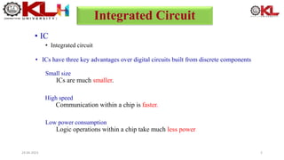
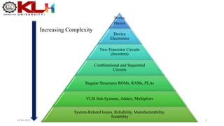
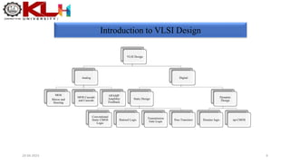
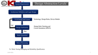
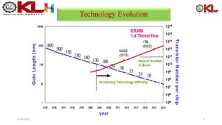
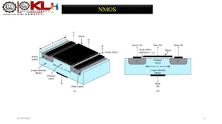
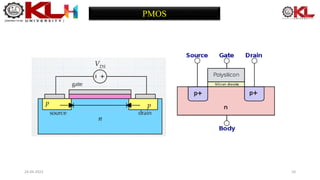
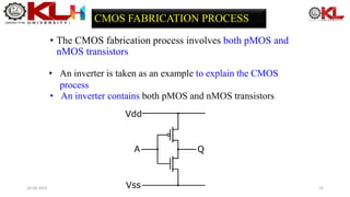
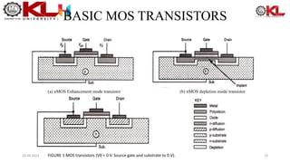
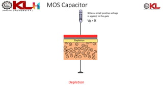
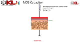
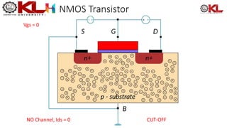
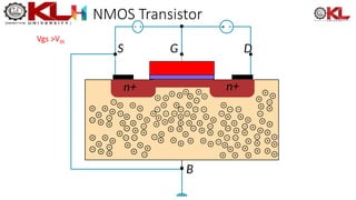
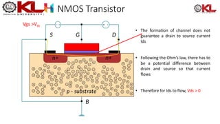
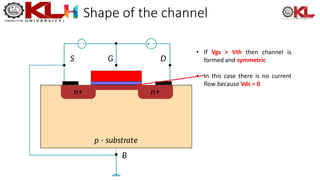
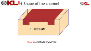
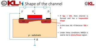
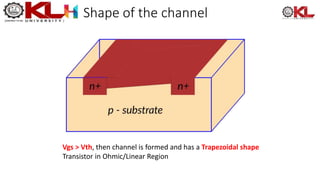
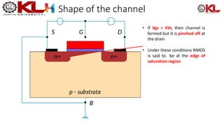
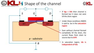
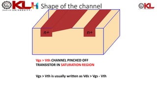
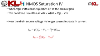
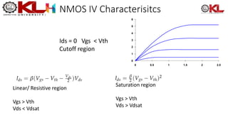
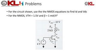
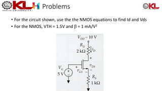
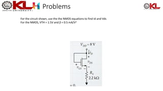
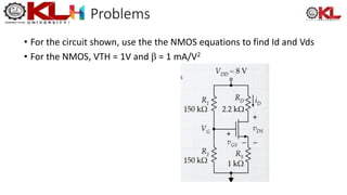
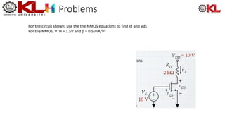
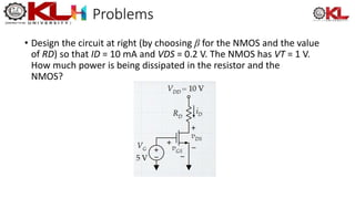
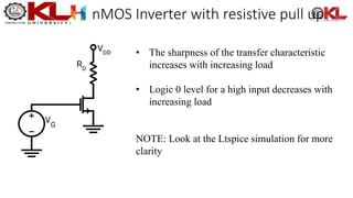
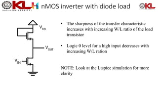
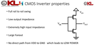
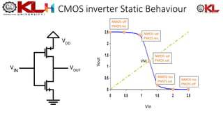
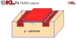
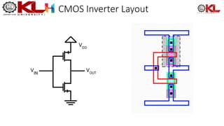
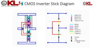
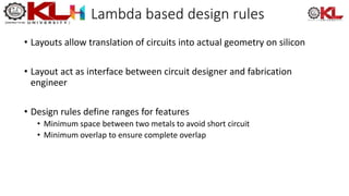
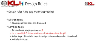
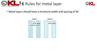
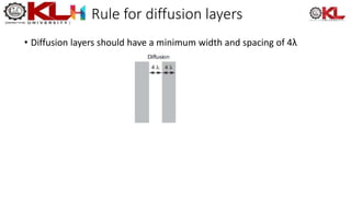
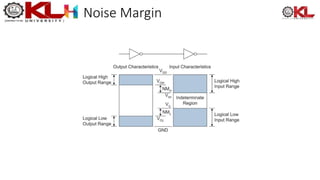
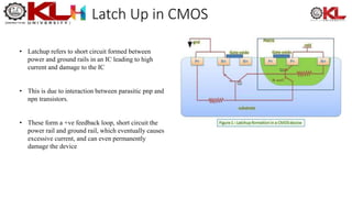
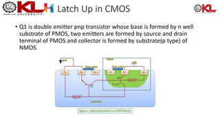
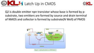
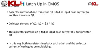
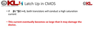
1. VLSI Design
Dr. Vijay Rao Kumbhare
Assistant Professor (ECE)
K L University, Hyderabad
Session Outcome: 1 Remember the IC era and Understand the MOS transistor analysis
Session No. 03
22-12-2022
1
24-04-2023
2. Integrated Circuit
• IC
• Integrated circuit
2
24-04-2023
• ICs have three key advantages over digital circuits built from discrete components
Small size
ICs are much smaller.
High speed
Communication within a chip is faster.
Low power consumption
Logic operations within a chip take much less power
11. Fabrication
• nMOS - Early process with which only nMOS transistors
could be fabricated
11
24-04-2023
• pMOS - Similar to nMOS process, but only pMOS transistors
could be fabricated
• CMOS - Complementary Metal Oxide Semiconductor process with which
both pMOS and nMOS could be fabricated on the same substrate
12. CMOS FABRICATION PROCESS
• The CMOS fabrication process involves both pMOS and
nMOS transistors
12
24-04-2023
• An inverter is taken as an example to explain the CMOS
process
• An inverter contains both pMOS and nMOS transistors
13. BASIC MOS TRANSISTORS
(a) nMOS Enhancement mode transistor (b) nMOS depletion mode transistor
FIGURE 1 MOS transistors (V0 = 0 V. Source gate and substrate to 0 V). 13
24-04-2023
20. NMOS Transistor
• The formation of channel does not
guarantee a drain to source current
Ids
• Following the Ohm’s law, there has to
be a potential difference between
drain and source so that current
flows
• Therefore for Ids to flow, Vds > 0
Vgs >Vth
21. Shape of the channel
• If Vgs > Vth then channel is
formed and symmetric
• In this case there is no current
flow because Vds = 0
22. Shape of the channel
Vgs > Vth CHANNEL SYMMETRIC
23. Shape of the channel
• If Vgs > Vth, then channel is
formed and has a trapezoidal
shape
• In this case, Ids > 0 because Vds >
0
• Under these conditions NMOS is
said to be in ohmic/linear region
24. Shape of the channel
Vgs > Vth, then channel is formed and has a Trapezoidal shape
Transistor in Ohmic/Linear Region
25. Shape of the channel
• If Vgs > Vth, then channel is
formed but it is pinched off at
the drain
• Under these conditions NMOS
is said to be at the edge of
saturation region
26. Shape of the channel
• If Vgs > Vth then channel is
formed but it does not exist
till the drain region
• Under these conditions NMOS
is said to be in the saturation
region
• Even without channel formed
completely till the drain, the
current flows from drain to
source due to drift
• In saturation region, Ids is
independent of Vds
27. Shape of the channel
Vgs > Vth CHANNEL PINCHED OFF
TRANSISTOR IN SATURATION REGION
Vgs > Vth is usually written as Vds > Vgs - Vth
28. IV Characteristics
The IV Characteristics we derive now are from IDEAL Model
Too many secondary effects are neglected in this model
In Cut-off region Ids = 0
In Linear Region, Ids depends on
How much charge is in the channel?
How fast is the charge moving?
29. Channel Charge
MOS structure looks like parallel plate capacitor while
operating in inversion
Gate – oxide – channel
30. Carrier Velocity
• Charge is carried by electron in NMOS
• Carrier velocity v is proportional to lateral E-field between source and drain
•
•
• Time for the carriers to cross the channel
31. NMOS Linear IV
• NOW, we know
• How much charge is in the channel (QChannel)
• How much time each carrier takes to cross the channel
32. NMOS Saturation IV
• When Vgd < Vth channel pinches off at the drain region
• This condition is written as Vds > Vdsat = Vgs – Vth
• Now the drain source voltage no longer causes increase in current
34. Problems
• For the circuit shown, use the the NMOS equations to find Id and Vds
• For the NMOS, VTH = 1.5V and β = 1 mA/V2
35. Problems
• For the circuit shown, use the the NMOS equations to find Id and Vds
• For the NMOS, VTH = 1.5V and β = 1 mA/V2
36. Problems
For the circuit shown, use the the NMOS equations to find Id and Vds
For the NMOS, VTH = 1.5V and β = 0.5 mA/V2
37. Problems
• For the circuit shown, use the the NMOS equations to find Id and Vds
• For the NMOS, VTH = 1V and β = 1 mA/V2
38. Problems
For the circuit shown, use the the NMOS equations to find Id and Vds
For the NMOS, VTH = 1.5V and β = 0.5 mA/V2
39. Problems
• Design the circuit at right (by choosing β for the NMOS and the value
of RD) so that ID = 10 mA and VDS = 0.2 V. The NMOS has VT = 1 V.
How much power is being dissipated in the resistor and the
NMOS?
40. nMOS Inverter with resistive pull up
• The sharpness of the transfer characteristic
increases with increasing load
• Logic 0 level for a high input decreases with
increasing load
NOTE: Look at the Ltspice simulation for more
clarity
41. nMOS inverter with diode load
• The sharpness of the transfer characteristic
increases with increasing W/L ratio of the load
transistor
• Logic 0 level for a high input decreases with
increasing W/L ration
NOTE: Look at the Ltspice simulation for more
clarity
42. CMOS Inverter properties
• Full rail to rail swing
• Low output impedance
• Extremely high input impedance
• Large Fanout
• No direct path from VDD to GND which leads to LOW POWER
43. CMOS inverter Static Behaviour
0
0.5
1
1.5
2
2.5
0 0.5 1 1.5 2 2.5
VIn
Vout
NMOS off
PMOS res
NMOS sat
PMOS res
NMOS sat
PMOS sat
NMOS res
PMOS sat NMOS res
PMOS off
VM
44. Transient Behaviour
Vin = 0
Low to High Transition
Propagation Delay α Rp Cout
Vin = 1
HIGH to Low Transition
Propagation Delay α Rn Cout
45. Transient Behaviour
• How can we build a faster inverter?
Keeping the Output capacitance small
Decreasing ON resistance of the transistor
ON resistance decreases with increasing W/L ratio of the transistor
46. Transient Behaviour
• When Both PMOS and NMOS are symmetric, VM = VDD/2
• Symmetrical when W/L of PMOS is roughly twice that of NMOS
• This is because the mobility of electrons is roughly twice that of holes
• The inverter can be skewed to be either high or low
• Note: Look into the CMOS inverter characteristics file for better
understanding
51. Scaling
• Technology shrinks by 0.7 times every generation
• With every generation we can integrate 2x more functionality
• Cost of a function decreases by 2x
• There is a need for better design
52. Supply Voltage Scaling
• Continuing technology scaling forces the supply voltages to reduce at
rates similar to device dimensions
• For example 180 nm 1.8 V and for 90 nm 1.1 V
• How does it affect CMOS inverter ?
• Reducing VDD improves transition region gain
• But gain degrades for very low supply voltages
0
0.5
1
1.5
2
2.5
0 0.5 1 1.5 2 2.5
0
0.05
0.1
0.15
0.2
0 0.05 0.1 0.15 0.2
53. Lambda based design rules
• Layouts allow translation of circuits into actual geometry on silicon
• Layout act as interface between circuit designer and fabrication
engineer
• Design rules define ranges for features
• Minimum space between two metals to avoid short circuit
• Minimum overlap to ensure complete overlap
54. Design Rules
• Design rules have two major approaches
• Micron rules
• Absolute dimensions are discussed
• Lambda rules
• Depend on a single parameter λ
• λ is usually 0.5 times minimum drawn transistor length
• Advantage of Lambda rules is design rules can be scaled based on λ
• Widely accepted
55. Rules for metal layer
• Metal layers should have a minimum width and spacing of 4λ
56. Rule for diffusion layers
• Diffusion layers should have a minimum width and spacing of 4λ
57. Rules for polysilicon layer
• Polysilicon to have a minimum width of 2λ
• Minimum spacing between two polys must be 3λ
58. Rules for contacts
• Contacts must be 2λ by 2λ and should be surrounded by 1λ on the
layers above and below
59. Rule for spacing between contacts
• Contacts must have a spacing of 3λ from each other
63. Latch Up in CMOS
• Latchup refers to short circuit formed between
power and ground rails in an IC leading to high
current and damage to the IC
• This is due to interaction between parasitic pnp and
npn transistors.
• These form a +ve feedback loop, short circuit the
power rail and ground rail, which eventually causes
excessive current, and can even permanently
damage the device
64. Latch Up in CMOS
• Q1 is double emitter pnp transistor whose base is formed by n well
substrate of PMOS, two emitters are formed by source and drain
terminal of PMOS and collector is formed by substrate(p type) of
NMOS.
65. Latch Up in CMOS
Q2 is double emitter npn transistor whose base is formed by p-
substrate, two emitters are formed by source and drain terminal
of NMOS and collector is formed by substrate(N Well) of PMOS
66. Latch Up in CMOS
• Collector current of one transistor Q1 is fed as input base current to
another transistor Q2
• Collector current of Q2, Ic2 = β2 * Ib2
• This collector current Ic2 is fed as input base current Ib1 to transistor
Q1
• In this way both transistors feedback each other and the collector
current of each goes on multiplying.
67. Latch Up in CMOS
• If β1 *β2 >=1, both transistors will conduct a high saturation
current
• This current eventually becomes so large that it may damage the
device.
Editor's Notes
or equivalently Vgs > Vgd
and Vgs = Vgd,
In a MOS transistor, the channel shape is a function of two voltages: Vgs and Vgd
and Vgs = Vgd
Vgd
In a MOS transistor, the channel shape is a function of two voltages: Vgs and Vgd
Vgd >
and Vgd = Vth
In a MOS transistor, the channel shape is a function of two voltages: Vgs and Vgd