Downloaded 157 times


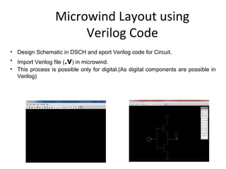


The document discusses the VLSI lab and its goals of designing and simulating CMOS inverter circuits using CAD tools. It describes the necessary hardware, software, and foundry resources needed. The design steps are outlined as schematic creation, layout design, DRC checks, parasitic extraction, and post-layout simulation. A list of experiments is provided focusing on logic gates, flip flops, multiplexers, and sequential circuits. The document also discusses the Microwind tool for circuit layout and simulation and provides tutorials on MOS devices and design rules for the layout process.