Downloaded 2,174 times
![Stick Diagram Intermediate representation between the transistor level and the mask (layout) level. Gives topological information (identifies different layers and their relationship) Assumes that wires have no width. It is possible to translate stick diagram automatically to layout with correct design rules. [Ref]: 教育部顧問室 「超大型積體電路與系統設計」教育改進計畫 EDA 聯盟 – 推廣課程 Chap.1](https://image.slidesharecdn.com/lect5stickdiagramlayoutrules-1226994677707873-9/85/lect5_Stick_diagram_layout_rules-8-320.jpg)
![Stick Diagram 1. When the same material (on the same layer) touch or cross, they are connected and belong to the same electrical node. 2. When polysilicon crosses N or P diffusion , an N or P transistor is formed. Polysilicon is drawn on top of diffusion. Diffusion must be drawn connecting the source and the drain. Gate is automatically self-aligned during fabrication. [Ref]: 教育部顧問室 「超大型積體電路與系統設計」教育改進計畫 EDA 聯盟 – 推廣課程 Chap.1](https://image.slidesharecdn.com/lect5stickdiagramlayoutrules-1226994677707873-9/85/lect5_Stick_diagram_layout_rules-9-320.jpg)
![Stick Diagram 3. When a metal line needs to be connected to one of the other three conductors, a contact cut ( via ) is required. [Ref]: 教育部顧問室 「超大型積體電路與系統設計」教育改進計畫 EDA 聯盟 – 推廣課程 Chap.1](https://image.slidesharecdn.com/lect5stickdiagramlayoutrules-1226994677707873-9/85/lect5_Stick_diagram_layout_rules-10-320.jpg)
![CMOS Inverter Stick Diagrams Basic layout More area efficient layout [Ref]: 教育部顧問室 「超大型積體電路與系統設計」教育改進計畫 EDA 聯盟 – 推廣課程 Chap.1](https://image.slidesharecdn.com/lect5stickdiagramlayoutrules-1226994677707873-9/85/lect5_Stick_diagram_layout_rules-13-320.jpg)
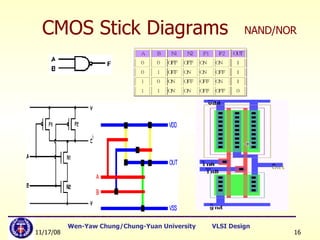
![[Ref]: 教育部顧問室 「超大型積體電路與系統設計」教育改進計畫 EDA 聯盟 – 推廣課程 Chap.1 CMOS Stick Diagrams NAND](https://image.slidesharecdn.com/lect5stickdiagramlayoutrules-1226994677707873-9/85/lect5_Stick_diagram_layout_rules-17-320.jpg)
![CMOS Stick Diagrams [Ref]: 教育部顧問室 「超大型積體電路與系統設計」教育改進計畫 EDA 聯盟 – 推廣課程 Chap.1 NOR](https://image.slidesharecdn.com/lect5stickdiagramlayoutrules-1226994677707873-9/85/lect5_Stick_diagram_layout_rules-20-320.jpg)
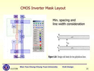
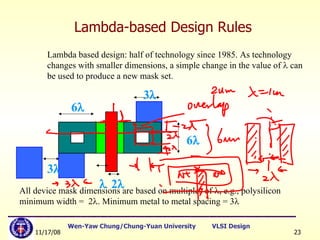
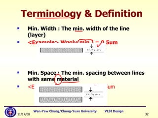
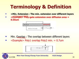
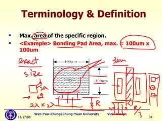
![Design Rules(1) Layout rules are used for preparing the masks for fabrication. Fabrication processes have inherent limitations in accuracy. Design rules specify geometry of masks to optimize yield and reliability (trade-offs: area, yield, reliability). Three major rules: Wire width: Minimum dimension associated with a given feature. Wire separation: Allowable separation. Contact: overlap rules. [Ref]: 教育部顧問室 「超大型積體電路與系統設計」教育改進計畫 EDA 聯盟 – 推廣課程 Chap.1](https://image.slidesharecdn.com/lect5stickdiagramlayoutrules-1226994677707873-9/85/lect5_Stick_diagram_layout_rules-30-320.jpg)
![Design Rules(2) Two major approaches: “ Micron” rules: stated at micron resolution. rules: simplified micron rules with limited scaling attributes. may be viewed as the size of minimum feature. Design rules represents a tolerance which insures very high probability of correct fabrication (not a hard boundary between correct and incorrect fabrication). Design rules are determined by experience. [Ref]: 教育部顧問室 「超大型積體電路與系統設計」教育改進計畫 EDA 聯盟 – 推廣課程 Chap.1](https://image.slidesharecdn.com/lect5stickdiagramlayoutrules-1226994677707873-9/85/lect5_Stick_diagram_layout_rules-31-320.jpg)
![SCMOS Design Rules [Ref]: 教育部顧問室 「超大型積體電路與系統設計」教育改進計畫 EDA 聯盟 – 推廣課程 Chap.1](https://image.slidesharecdn.com/lect5stickdiagramlayoutrules-1226994677707873-9/85/lect5_Stick_diagram_layout_rules-39-320.jpg)
![MOSIS Layout Design Rules MOSIS design rules (SCMOS rules) are available at http://www.mosis.org. 3 basic design rules: Wire width Wire separation Contact rule MOSIS design rule examples [Ref]: 教育部顧問室 「超大型積體電路與系統設計」教育改進計畫 EDA 聯盟 – 推廣課程 Chap.1](https://image.slidesharecdn.com/lect5stickdiagramlayoutrules-1226994677707873-9/85/lect5_Stick_diagram_layout_rules-40-320.jpg)
![Concluding Remarks Milestones technology in silicon era Transistor Integrated Circuits CMOS Technology Key weapons in SOC era Design Automation Design Reuse Breakthrough techniques in design automation Simulation (e.g., SPICE, Verilog-XL, etc.) Automatic Placement and Routing (APR) Logic Synthesis (e.g., Design Compiler) Formal Verification Test Pattern Generation It is EDA that pushes the IC design technology forward ! [Ref]: 教育部顧問室 「超大型積體電路與系統設計」教育改進計畫 EDA 聯盟 – 推廣課程 Chap.1](https://image.slidesharecdn.com/lect5stickdiagramlayoutrules-1226994677707873-9/85/lect5_Stick_diagram_layout_rules-46-320.jpg)
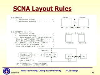
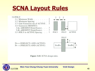
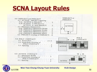
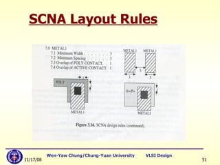
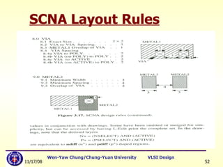
![SCNA Layout Rules [Ref.] John P. Uyemura, “Physical Design of CMOS Integrated Circuits Using L-EDIT”, PWS Publishing Company, 1995.](https://image.slidesharecdn.com/lect5stickdiagramlayoutrules-1226994677707873-9/85/lect5_Stick_diagram_layout_rules-47-320.jpg)

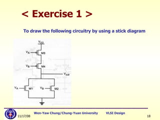
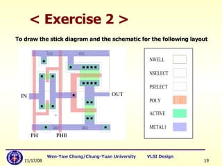
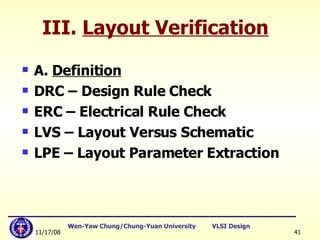
The document discusses stick diagrams and design rules for VLSI layout. It begins by explaining stick diagrams, which provide topological information to represent circuits between the schematic and layout levels. Examples of stick diagrams for CMOS inverters and other gates are shown. The document then covers design rules, which specify geometries and spacing to optimize yield and reliability. Examples of minimum widths, spacings, and other rules are discussed. The end discusses layout verification using techniques like DRC, LVS, and extraction to check for errors and ensure consistency between schematic and layout.


