MOS and CMOS circuit design involves several key concepts:
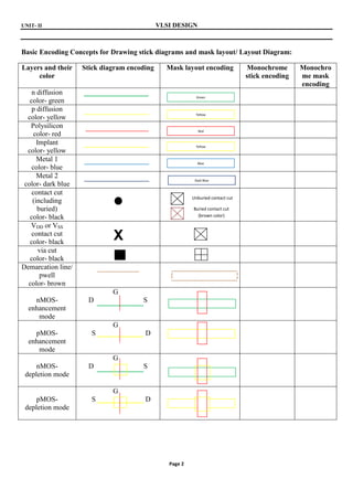
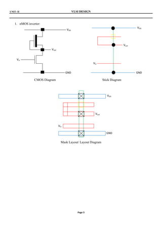
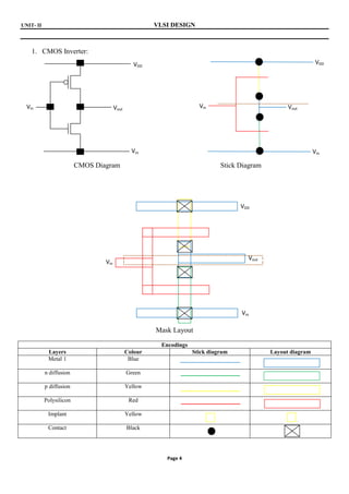
1. Circuits are formed from diffusion, polysilicon, and metal layers isolated by silicon dioxide. Transistors form where polysilicon crosses diffusion regions.
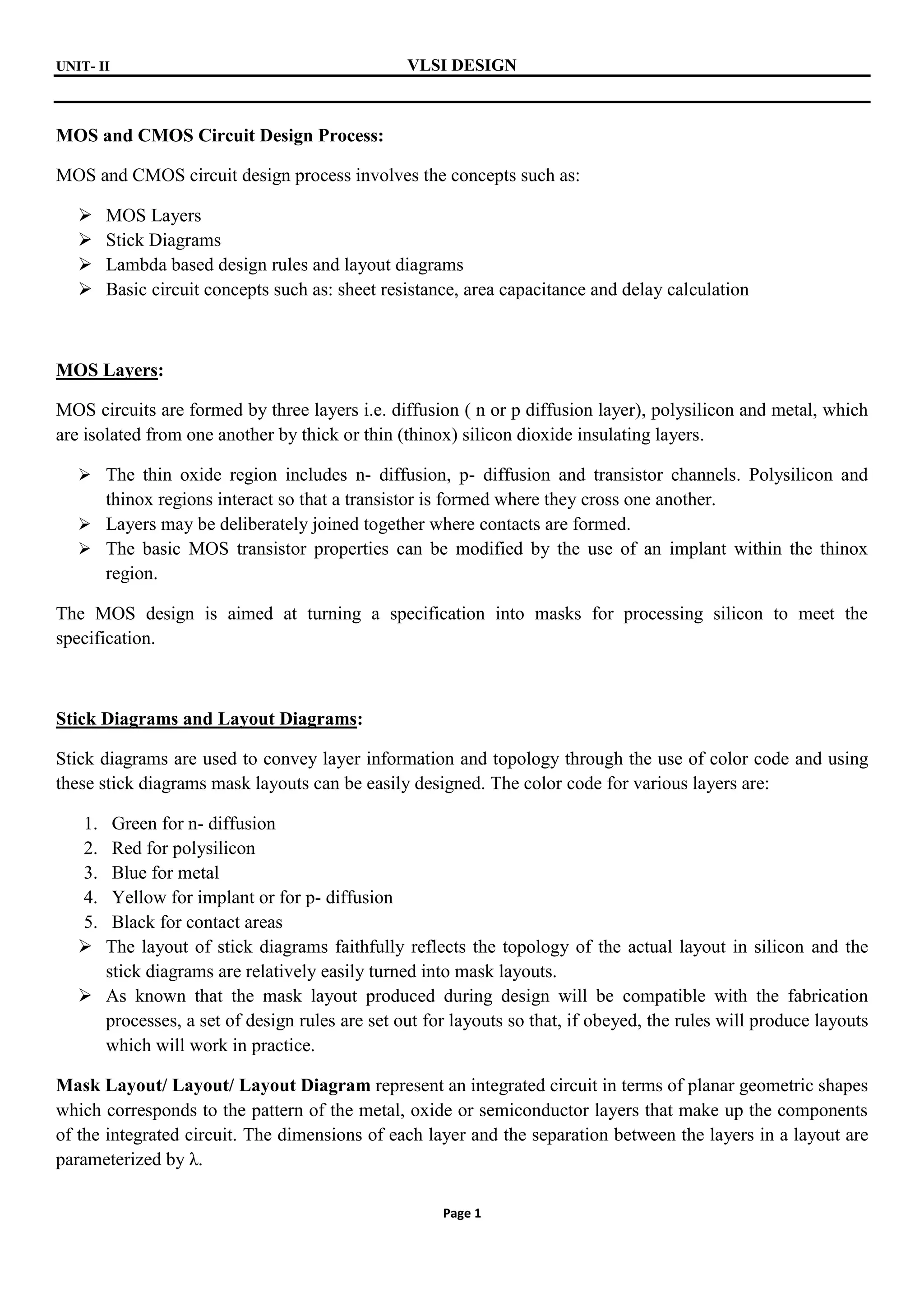
2. Stick diagrams use colors to represent layers and convey topology. Layout diagrams translate stick diagrams into mask patterns matching silicon topology.
3. Design rules parameterized by λ ensure mask layouts produce working circuits across fabrication processes by specifying minimum widths, separations, and extensions in units of λ.
This document discusses the design of high performance printed circuit boards. It covers topics such as PCB design flow, mechanical design considerations, electrical considerations like impedance and noise, capacitor advantages and disadvantages, microstrip and signal trace configurations, cross-talk control techniques, termination methods, and guidelines for layout and EMI reduction. The goal is to minimize delays, noise, and reliability issues through careful mechanical and electrical design.
The composition and packaging of integrated circuitsVinsion Chan
Integrated circuits (ICs) are electronic circuits formed on a small chip of semiconductor material. They consist of transistors, resistors, capacitors, and other components connected together to form complete circuits. ICs can be categorized in several ways, including by function (analog, digital, or mixed-signal), manufacturing process (semiconductor or thin-film), integration level (small-scale to very large-scale), conductive type (bipolar or unipolar), application (computers, communications, etc.), and physical appearance (circular, flat, or dual-in-line package). Modern ICs allow many circuit elements to be miniaturized and placed on a single semiconductor chip, improving performance, reliability, and energy efficiency.
1) The document discusses the capacitance-voltage characteristics of a MOS capacitor. It derives expressions for surface charge, depletion approximation, onset of strong inversion, and calculation of capacitance in different regimes.
2) Graphs of capacitance versus voltage are shown and explained for accumulation, flat-band, depletion, and inversion conditions.
3) The differences between low-frequency and high-frequency approximations are described based on whether inversion or depletion charge can follow the applied signal.
Stick diagrams are used to represent VLSI layouts in an abstract way, showing the relative placements and connections between different layers like polysilicon, diffusion, and metal layers. They follow rules like only allowing electrical contact between sticks of the same layer when they cross. Euler graphs can be used to determine if a CMOS logic gate layout is possible by finding an Euler path through the graph. MOS transistors have different operating regions depending on voltages, and their I-V characteristics can be modeled based on factors like channel charge and carrier mobility. Parasitic capacitances also exist between diffusion regions, gates, and the substrate.
Ericsson WCDMA W14 Radio Network Functionality.pdfHuong Tra Tran
This document provides a summary of WCDMA radio network functionality including:
- An overview of HSPA features such as short transmission time interval and adaptive modulation that improve data rates.
- A description of the main functionality areas of WCDMA including idle mode, radio connection supervision, power control, capacity management and mobility.
- Details on specific power control functions including open loop power control and inner and outer loop power control.
- Explanations of cell selection and reselection processes, and radio link failure detection.
The document is intended as a training manual for understanding the key components and operations of WCDMA radio networks.
Very Large Scale Integration (VLSI) is a solid career choice and offers job opportunities for ECE freshers pursuing core employment. In India and overseas, VLSI provides a variety of employment roles featuring outstanding professional growth and salary incentives.
The document discusses network-on-chip (NoC) technology. NoC uses a packet switched network approach to connect intellectual property cores on a chip. It provides advantages over traditional bus-based interconnects like higher bandwidth, energy efficiency, and scalability. NoCs operate using a layered approach with physical, transport, and transaction layers. Common routing algorithms for NoCs include dimension order routing, XY routing, fully adaptive routing, and minimal adaptive routing. NoCs allow for modular and reconfigurable integration of IP cores from different vendors.
Freq response of CE and CC discrete circuitsJavaria Haseeb
The document discusses frequency response and how capacitors affect an amplifier's response. It notes that an ideal amplifier's gain should be independent of frequency, but in practice amplifiers only act linearly over a range of frequencies defined by lower (fL) and upper (fH) cut-off frequencies. Capacitors introduce poles that define these cut-off frequencies. The document examines how to determine which capacitors contribute to fL and fH by analyzing the circuit with different capacitor conditions. It also discusses the capacitive effects in transistors that contribute to the high-frequency response roll-off.
Stick Diagram and Lambda Based Design RulesTahsin Al Mahi
This presentation discusses stick diagrams and lambda-based design rules for VLSI system design. It begins with an overview of the top-down design hierarchy and then defines stick diagrams as a way to represent different layers of a layout using colors or monochrome lines. Common stick encodings are presented along with examples of drawing a CMOS inverter. Design rules are then covered, with lambda serving as a size-independent unit and rules specifying dimensions for wires, transistors, and contacts between layers. The goal is to convey key layer information and spacing requirements for mask layouts in a standardized way.
This document discusses integrated circuits (ICs) and their manufacturing. It describes how ICs are miniature circuits on semiconductor chips that contain components like transistors and diodes. The two main techniques for manufacturing ICs are the bipolar technique and metal oxide semiconductor (MOS) technique. It also discusses different categories of digital ICs based on their scale of integration, including small-scale, medium-scale, large-scale, and very-large scale integration circuits. Factors that influence IC technology choices are also summarized.
The document discusses PCI (Physical Cell Identity) planning in LTE networks. It describes the cell search process where the UE detects the PCI from the PSS and SSS. The PCI is used to determine the location of reference signals and avoid interference. The document recommends strategies for PCI planning such as assigning color groups to sectors and code groups to sites to avoid conflicting PCI combinations in adjacent cells. It also discusses tools to analyze potential PCI interference and make changes to mitigate issues.
The document is a service manual that provides instructions for repairing Nokia phone models RM-133 and RM-132. It contains information about the phone specifications and components. The manual instructs technicians on general repair procedures, accessing repair documentation on Nokia's website, disassembling the phones, troubleshooting issues, and includes exploded views of the phone components. It aims to help service technicians at Levels 1 and 2 carry out repairs to Nokia products.
Define location of Preplaced cells(http://www.vlsisystemdesign.com/PD-Flow.php)VLSI SYSTEM Design
https://www.udemy.com/vlsi-academy
During placement and routing, most of the placement tools, place/move logic cells based on floorplan specifications. Some of the important or critical cell's locations has to be pre-defined before actual placement and routing stages. The critical cells are mostly the cells related to clocks, viz. clock buffers, clock mux, etc. and also few other cells such as RAM's, ROM,s etc. Since, these cells are placed in to core before placement and routing stage, they are called 'preplaced cells'.
The document is a technical presentation about the MINI-LINK 6352 product from Ericsson. It discusses E-band spectrum characteristics, features of the MINI-LINK 6352 such as capacity, interfaces and antennas. It also covers use cases, design considerations and site solutions such as power and backhaul options.
This document discusses transmission lines and their parameters. It begins by introducing transmission lines as guided structures that direct the propagation of energy from a source to a load. It then discusses the key parameters used to describe transmission lines - resistance, inductance, conductance and capacitance per unit length. It provides examples of how electromagnetic waves propagate through transmission lines and derives the transmission line equations. It also covers input impedance, standing wave ratio, power, and gives examples of calculating transmission line properties. The document concludes by discussing microstrip transmission lines.
The document discusses DDR noise interference issues in cellular devices. It notes that DDR noise can desense channels near half the DDR clock frequency and that this noise can couple from the DDR chip to the baseband chip and then to RF components. It recommends using an LC filter near the baseband chip to mitigate this issue but notes the capacitor cannot be too large or it may degrade the sensitivity of wide bandwidth LTE signals by attenuating the I/Q signals.
The document provides information about a paper presentation on VLSI design and fabrication by two students. It includes an outline of topics to be covered such as introduction to VLSI, MOS transistors, CMOS circuits, and fabrication. The presentation aims to provide an introduction to VLSI design including how MOS transistors work and are used to build logic gates, as well as the process of designing masks and layouts for chips. It also gives an overview of the fabrication process used to manufacture chips.
The United Arab Emirates has a power production capacity of 18.74 GW but lacks capacity during peak seasonal times due to increasing demand. It also lacks natural gas resources. The Gulf Cooperation Council began developing a regional power grid to help meet demand. Phase 3 of this grid will connect the southern system of the UAE. The UAE also plans to build 4 nuclear reactors to generate additional power. Electric power is transmitted through overhead transmission lines suspended by steel lattice towers for long distances. The document discusses the anatomy of transmission towers and the different types, configurations, and design considerations for efficient power transmission.
Propagation Effects and Their Impact on Satellite-Earth Links: Introduction,
Quantifying attenuation and depolarization,
Propagation effects that are not associated with hydrometeors, Prediction of rain attenuation,
Prediction of XPD,
Propagation impairments countermeasures.
The document discusses placement in physical design. It describes placement as assigning positions to predesigned cells on a chip without overlapping to optimize objectives like minimizing area and interconnects. It discusses different placement types, formulates the placement problem, and describes algorithms like partitioning-based placement, simulated annealing placement, and iterative placement methods.
I have prepared it to create an understanding of delay modeling in VLSI.
Regards,
Vishal Sharma
Doctoral Research Scholar,
IIT Indore
vishalfzd@gmail.com
CMOS analog IC Design presentation.pptxAkash588342
The document summarizes the CS stage with source degeneration. It describes how adding a degeneration resistor RS in series with the source terminal makes the input device more linear. As the input voltage increases, the voltage drop across RS increases, making variations in drain current smoother. Source degeneration reduces the dependence of gain on transconductance. It also increases the output resistance of the circuit by boosting the transistor's output resistance ro by a factor that includes RS. The document provides analysis of how source degeneration affects transconductance, voltage gain, and output resistance using small-signal models.
Design And Analysis of Charge Pump for PLL at 90nm CMOS technologyRavi Chandra
The document discusses the design and analysis of a charge pump for phase locked loop applications in 90nm CMOS technology. It begins with an introduction to charge pumps and their use in PLLs. It then outlines the objectives of designing an optimized charge pump with reduced charge sharing and current mismatching. The methodology discusses studying conventional charge pump design, designing a proposed charge pump using operational amplifiers for current matching, and analyzing effects of process, voltage and temperature variation on output voltage. Simulation results show the proposed design has less current mismatching, wider output voltage range, and is more immune to PVT variation compared to a conventional design.
IC Design of Power Management Circuits (IV)Claudia Sin
by Wing-Hung Ki
Integrated Power Electronics Laboratory
ECE Dept., HKUST
Clear Water Bay, Hong Kong
www.ee.ust.hk/~eeki
International Symposium on Integrated Circuits
Singapore, Dec. 14, 2009
1. The document discusses GPS signal power received on Earth from satellites in low Earth orbit. It calculates the free space path loss over the 20,000 km distance to be approximately 180.4 dB.
2. GPS satellites transmit signals at 25.6 Watts with a 13 dBi antenna gain, resulting in an effective isotropic radiated power of around 500 Watts or 27 dBW.
3. Accounting for the 180.4 dB free space path loss and 2 dB of atmospheric loss, the received power at the Earth's surface is calculated to be -155 dBW, which has a 5 dB margin above the specification of -160 dBW.
This document provides an overview of the ASIC design process, which includes the following main steps:
1. Front-end design including market research, specification, architecture, and RTL design.
2. Verification of the RTL code by verification engineers.
3. Synthesis of the RTL code into a gate-level netlist, followed by equivalence checking.
4. Physical design including placement and routing of standard cells, followed by extraction of parasitic components and timing analysis.
5. Physical verification including design rule checking and layout vs schematic checking.
Optimized Local I/O ESD Protection for SerDes In Advanced SOI, BiCMOS and Fin...Sofics
Sofics presentation (B2.2) at the 1st International EOS/ESD Symposium on Design and System (IEDS). IEDS is dedicated to the fundamental understanding of issues related to electrostatic discharge on design and system and the application of this knowledge to the solution of problems.
Semiconductor companies are developing ever faster interfaces to satisfy the need for higher data throughputs. However, the parasitic capacitance of the traditional ESD solutions limits the signal frequency. This paper demonstrates low-cap Analog I/Os for high speed SerDes (28Gbps to 112Gbps) circuits created in advanced BiCMOS, SOI and FinFET nodes.
This document discusses MOS and BiCMOS circuit design processes. It describes the layers used in MOS circuits and provides color encodings for stick diagrams. Stick diagrams capture layer information through simple diagrams and act as an interface between symbolic circuits and layouts. The document outlines the NMOS and CMOS design processes, including rules for drawing stick diagrams and placing transistors. It also covers design rules and lambda-based rules for layout dimensions and separations. Contact cuts and buried contacts are discussed for making electrical connections between layers.
This document discusses design processes and rules for MOS and BiCMOS circuit design. It provides details on:
1) MOS layers including n-diffusion, p-diffusion, polysilicon, and metal layers used to form transistors. BiCMOS adds layers for bipolar transistors.
2) Stick diagrams which use color coding to represent different layers and abstract chip layout from transistor schematics.
3) Design rules including lambda-based rules that specify minimum feature sizes and separations to translate circuit designs into mask layouts that can be fabricated.
This presentation discusses the Lambda based design rules for drawing the layouts. The spacing between ltwo layers, extent if of overlap, minimum dimensions of each layer etc are decided by the lambda based design rules. the separation between metal and poly, poly and diffusion , width of metal etc
5164 2015 YRen Two-Dimensional Field Effect TransistorsYi Ren
This document provides an introduction to two-dimensional field effect transistors (2D FETs). It first discusses the limitations of conventional FETs as their size is reduced according to Moore's Law. 2D FETs are proposed as a way to continue increasing transistor density by using atomically thin 2D materials as the channel layer. The document then discusses properties of graphene and transition metal dichalcogenides, which are common materials used in 2D FET channels. Finally, examples of 2D FETs using MoS2 and other materials as the channel layer are described.
Vlsi design notes(1st unit) according to vtu syllabus.(BE)instrumentation_vtu
This document provides an introduction to MOS technology and CMOS fabrication. It discusses Moore's Law, the doubling of transistors every 18 months. It then describes the basic nMOS and pMOS transistor structures and their modes of operation. The document outlines the nMOS and CMOS fabrication processes, including masking, doping, and interconnection steps. It also introduces BiCMOS technology which combines bipolar and CMOS to provide higher speeds, and compares the properties of bipolar and CMOS technologies.
This document discusses the layout design process for CMOS logic gates. It begins by outlining the design flow, from initial circuit topology and transistor sizing to layout drawing, extraction, simulation and iteration. Key points include:
- Layout directly impacts performance via parasitic capacitances and resistances.
- Design rules constrain layout geometries and ensure fabrication yield.
- A CMOS inverter layout is designed step-by-step to demonstrate design rule influences.
- Stick diagrams simplify initial topology exploration before full layout.
- Multiple metal layers provide increased interconnect flexibility in layouts.
Nanometer layout handbook at high speed designMinho Park
I made this contents for whom is about to layout own's IC design. I think it would be helpful to consider layouts about high speed Rx / Tx.
Specially it was aimed giga hertz bandwidth I/O with its ESD protection (I am still working on that items to rearrange with my knowledge to my experiences)
I showed up all references and all images (except originals) are belong to own's copy rights.
Design of miniaturized patch crossover based on superformula slot shapesIJECEIAES
In this paper, miniaturized microstrip crossover circuits are proposed using slots shapes obtained using the superformula. The design starts by using a conventional half-wavelength square patch crossover. For miniaturization purposes, different superformula slot shapes are introduced on the square patch. The proposed crossovers are designed to operate at 2.4 GHz using a 0.8 mm thick FR-4 substrate with a relative permittivity of 4.4. The designs are simulated using the high frequency structure simulator (HFSS). One of the miniaturized designs is fabricated and its scattering parameters are measured using a vector network analyzer. Simulated and measured results agree very well. At the design frequency, the measured input port matching is better than ˗19 dB, while 𝑆12, 𝑆13 and 𝑆14 have the values of ˗12 dB, ˗2.2 dB and ˗10 dB, respectively. Furthermore, a 71% size reduction is achieved as compared to the conventional crossover area.
This paper evaluates the confinement loss of different photonic crystal fibers by varying the size and shape of holes in the fiber design. Several fiber designs are modeled using the finite-difference time-domain method, including varying the number of rings of holes, mixing elliptical shaped holes, and varying hole sizes. The design with the lowest confinement loss has two inner rings of elliptical shaped holes, with a confinement loss of 0.097459236 dB/km at a wavelength of 1.55μm. In general, designs with elliptical holes or fewer rings of holes exhibited lower confinement loss than designs with circular holes or more rings of holes.
Analysis Of 3C-Sic Double Implanted MOSFET With Gaussian Profile Doping In Th...IJRES Journal
The present work aims at the design of 3C-SiC Double Implanted Metal Oxide Semiconductor Field Effect Transistor (DIMOSFET) with Gaussian doping profile in drift region for high breakdown voltages. By varying the device height ‘h’, function constant m and peak concentration 𝑁0, analysis has been done for an optimum profile for high breakdown voltage. With Gaussian profile peak concentration 𝑁0 = 1016 𝑐𝑚−3 at drain end and m as 1.496 ×10⁻²cm, highest breakdown voltage of 6.84kV has been estimated with device height of 200μm.
Electrical characterization of semiconductor-insulator interfaces in VLSI:ULS...Dang Trang
The document summarizes an electrical engineering student's research project characterizing semiconductor-insulator interfaces in VLSI/ULSI technology. The student fabricated metal-oxide-silicon capacitors using hafnium oxide and silicon dioxide gate dielectrics. Through capacitance-voltage measurements, the student extracted the dielectric constants of the materials and found the hafnium oxide k-value matched reported values between 18-25. Interface charges in the hafnium oxide caused shifts in the flat-band voltage. Overall, using high-k hafnium oxide allowed thicker dielectric layers while maintaining capacitance, reducing leakage currents.
International Journal of Engineering Research and Applications (IJERA) is a team of researchers not publication services or private publications running the journals for monetary benefits, we are association of scientists and academia who focus only on supporting authors who want to publish their work. The articles published in our journal can be accessed online, all the articles will be archived for real time access.
Our journal system primarily aims to bring out the research talent and the works done by sciaentists, academia, engineers, practitioners, scholars, post graduate students of engineering and science. This journal aims to cover the scientific research in a broader sense and not publishing a niche area of research facilitating researchers from various verticals to publish their papers. It is also aimed to provide a platform for the researchers to publish in a shorter of time, enabling them to continue further All articles published are freely available to scientific researchers in the Government agencies,educators and the general public. We are taking serious efforts to promote our journal across the globe in various ways, we are sure that our journal will act as a scientific platform for all researchers to publish their works online.
The document provides an overview of physical design in VLSI. It discusses the VLSI design flow including specification, schematic design, layout, floorplanning, routing, and fabrication. It then describes layout considerations such as layers, design rules, DRC checks, and LVS checks. Examples of CMOS inverter, NAND and NOR gate layouts are shown. Optimization techniques for transistor sizing and drain connections are also covered. Different logic styles like pseudo-NMOS, dynamic CMOS, and domino logic are explained.
This document provides an overview of the physical design process for integrated circuits. It discusses the steps from schematic design to layout, including floorplanning, placement, routing, and design rule checking. Sample schematics and layouts are shown for basic gates like inverters, NAND gates, and transmission gates. Guidelines are provided for layout optimization to improve performance and density. The layout process involves translating the schematic into distinct layers and ensuring design rules are followed with respect to dimensions, spacing, and connectivity between layers.
vlsi qb.docx imprtant questions for all unitsnitcse
This document contains a question bank for the course EC3352: VLSI & Chip Design. It includes questions related to MOS transistor operation, CMOS logic, layout design rules, I-V characteristics, delay modeling, scaling concepts, and CMOS fabrication processes. Key topics covered are threshold voltage, body effect, latch-up, twin tub process, SOI process, Elmore delay model, logical effort, critical paths, and layout design rules such as lambda-based rules. Sample questions assess understanding of MOSFET parameters, transfer characteristics, non-ideal effects, noise margins, rise/fall times, and stick diagrams. Layout aspects include designing a 2-input NAND gate and explaining P-well and n
Design of Integrated LC Filter Using Multilayer Flexible Ferrite Sheets iosrjce
This document describes the design of an integrated LC filter using multilayer flexible ferrite sheets. Key points:
- The design aims to integrate an inductor and capacitor using ferrite sheets, which have both magnetic and dielectric properties, to reduce the size of filters in power electronic converters.
- The structure consists of a spiral inductor sandwiched between two ferrite sheets, acting as a magnetic core, with multiple ferrite layers above acting as a dielectric for a multilayer capacitor.
- Analytical equations are provided to calculate the inductance, capacitance, resistance and other parameters of the integrated LC component based on its geometric parameters and material properties.
- A design procedure is outlined to
This document describes the design of an integrated LC filter using multilayer flexible ferrite sheets. The structure consists of a spiral inductor sandwiched between two ferrite layers, which act as a magnetic core, and a multilayer capacitor above the ferrite layers. Analytical equations are provided to calculate the inductance, capacitance, and resistance of the design based on its geometric parameters and the material properties. A design procedure is outlined to size the components based on desired inductance and capacitance values. The integrated LC filter is simulated and a prototype is fabricated and tested to validate the analytical model.
VLSI stands for Very Large Scale Integration and refers to integrated circuits with over 100,000 transistors. The document discusses the history and progression of integration levels from SSI to VLSI to ULSI. It also describes the photolithography process used to etch circuit designs onto silicon wafers at the microscopic level needed for modern integrated circuits.
Welcome to International Journal of Engineering Research and Development (IJERD)IJERD Editor
This document discusses how different gate dielectric materials affect the threshold voltage of nanoscale MOSFETs. Simulations were conducted using MATLAB and SCHRED software to obtain C-V characteristics for MOSCAP structures with different dielectric materials (PTFE, Polyethylene, SiO2) and thicknesses. Threshold voltages were extracted from the C-V curves using classical, semi-classical, and quantum mechanical models. The results show that lower dielectric constant materials like PTFE reduce threshold voltage more than higher k materials like SiO2. PTFE is suggested as a suitable low-k material for developing MOSFETs and interconnects at the nanoscale.
Applications of artificial Intelligence in Mechanical Engineering.pdfAtif Razi
Historically, mechanical engineering has relied heavily on human expertise and empirical methods to solve complex problems. With the introduction of computer-aided design (CAD) and finite element analysis (FEA), the field took its first steps towards digitization. These tools allowed engineers to simulate and analyze mechanical systems with greater accuracy and efficiency. However, the sheer volume of data generated by modern engineering systems and the increasing complexity of these systems have necessitated more advanced analytical tools, paving the way for AI.
AI offers the capability to process vast amounts of data, identify patterns, and make predictions with a level of speed and accuracy unattainable by traditional methods. This has profound implications for mechanical engineering, enabling more efficient design processes, predictive maintenance strategies, and optimized manufacturing operations. AI-driven tools can learn from historical data, adapt to new information, and continuously improve their performance, making them invaluable in tackling the multifaceted challenges of modern mechanical engineering.
Discover the latest insights on Data Driven Maintenance with our comprehensive webinar presentation. Learn about traditional maintenance challenges, the right approach to utilizing data, and the benefits of adopting a Data Driven Maintenance strategy. Explore real-world examples, industry best practices, and innovative solutions like FMECA and the D3M model. This presentation, led by expert Jules Oudmans, is essential for asset owners looking to optimize their maintenance processes and leverage digital technologies for improved efficiency and performance. Download now to stay ahead in the evolving maintenance landscape.
Generative AI Use cases applications solutions and implementation.pdfmahaffeycheryld
Generative AI solutions encompass a range of capabilities from content creation to complex problem-solving across industries. Implementing generative AI involves identifying specific business needs, developing tailored AI models using techniques like GANs and VAEs, and integrating these models into existing workflows. Data quality and continuous model refinement are crucial for effective implementation. Businesses must also consider ethical implications and ensure transparency in AI decision-making. Generative AI's implementation aims to enhance efficiency, creativity, and innovation by leveraging autonomous generation and sophisticated learning algorithms to meet diverse business challenges.
https://www.leewayhertz.com/generative-ai-use-cases-and-applications/
Optimizing Gradle Builds - Gradle DPE Tour Berlin 2024Sinan KOZAK
Sinan from the Delivery Hero mobile infrastructure engineering team shares a deep dive into performance acceleration with Gradle build cache optimizations. Sinan shares their journey into solving complex build-cache problems that affect Gradle builds. By understanding the challenges and solutions found in our journey, we aim to demonstrate the possibilities for faster builds. The case study reveals how overlapping outputs and cache misconfigurations led to significant increases in build times, especially as the project scaled up with numerous modules using Paparazzi tests. The journey from diagnosing to defeating cache issues offers invaluable lessons on maintaining cache integrity without sacrificing functionality.
Blood finder application project report (1).pdfKamal Acharya
Blood Finder is an emergency time app where a user can search for the blood banks as
well as the registered blood donors around Mumbai. This application also provide an
opportunity for the user of this application to become a registered donor for this user have
to enroll for the donor request from the application itself. If the admin wish to make user
a registered donor, with some of the formalities with the organization it can be done.
Specialization of this application is that the user will not have to register on sign-in for
searching the blood banks and blood donors it can be just done by installing the
application to the mobile.
The purpose of making this application is to save the user’s time for searching blood of
needed blood group during the time of the emergency.
This is an android application developed in Java and XML with the connectivity of
SQLite database. This application will provide most of basic functionality required for an
emergency time application. All the details of Blood banks and Blood donors are stored
in the database i.e. SQLite.
This application allowed the user to get all the information regarding blood banks and
blood donors such as Name, Number, Address, Blood Group, rather than searching it on
the different websites and wasting the precious time. This application is effective and
user friendly.
DEEP LEARNING FOR SMART GRID INTRUSION DETECTION: A HYBRID CNN-LSTM-BASED MODELijaia
As digital technology becomes more deeply embedded in power systems, protecting the communication
networks of Smart Grids (SG) has emerged as a critical concern. Distributed Network Protocol 3 (DNP3)
represents a multi-tiered application layer protocol extensively utilized in Supervisory Control and Data
Acquisition (SCADA)-based smart grids to facilitate real-time data gathering and control functionalities.
Robust Intrusion Detection Systems (IDS) are necessary for early threat detection and mitigation because
of the interconnection of these networks, which makes them vulnerable to a variety of cyberattacks. To
solve this issue, this paper develops a hybrid Deep Learning (DL) model specifically designed for intrusion
detection in smart grids. The proposed approach is a combination of the Convolutional Neural Network
(CNN) and the Long-Short-Term Memory algorithms (LSTM). We employed a recent intrusion detection
dataset (DNP3), which focuses on unauthorized commands and Denial of Service (DoS) cyberattacks, to
train and test our model. The results of our experiments show that our CNN-LSTM method is much better
at finding smart grid intrusions than other deep learning algorithms used for classification. In addition,
our proposed approach improves accuracy, precision, recall, and F1 score, achieving a high detection
accuracy rate of 99.50%.
Software Engineering and Project Management - Introduction, Modeling Concepts...Prakhyath Rai
Introduction, Modeling Concepts and Class Modeling: What is Object orientation? What is OO development? OO Themes; Evidence for usefulness of OO development; OO modeling history. Modeling
as Design technique: Modeling, abstraction, The Three models. Class Modeling: Object and Class Concept, Link and associations concepts, Generalization and Inheritance, A sample class model, Navigation of class models, and UML diagrams
Building the Analysis Models: Requirement Analysis, Analysis Model Approaches, Data modeling Concepts, Object Oriented Analysis, Scenario-Based Modeling, Flow-Oriented Modeling, class Based Modeling, Creating a Behavioral Model.
Use PyCharm for remote debugging of WSL on a Windo cf5c162d672e4e58b4dde5d797...shadow0702a
This document serves as a comprehensive step-by-step guide on how to effectively use PyCharm for remote debugging of the Windows Subsystem for Linux (WSL) on a local Windows machine. It meticulously outlines several critical steps in the process, starting with the crucial task of enabling permissions, followed by the installation and configuration of WSL.
The guide then proceeds to explain how to set up the SSH service within the WSL environment, an integral part of the process. Alongside this, it also provides detailed instructions on how to modify the inbound rules of the Windows firewall to facilitate the process, ensuring that there are no connectivity issues that could potentially hinder the debugging process.
The document further emphasizes on the importance of checking the connection between the Windows and WSL environments, providing instructions on how to ensure that the connection is optimal and ready for remote debugging.
It also offers an in-depth guide on how to configure the WSL interpreter and files within the PyCharm environment. This is essential for ensuring that the debugging process is set up correctly and that the program can be run effectively within the WSL terminal.
Additionally, the document provides guidance on how to set up breakpoints for debugging, a fundamental aspect of the debugging process which allows the developer to stop the execution of their code at certain points and inspect their program at those stages.
Finally, the document concludes by providing a link to a reference blog. This blog offers additional information and guidance on configuring the remote Python interpreter in PyCharm, providing the reader with a well-rounded understanding of the process.
Home security is of paramount importance in today's world, where we rely more on technology, home
security is crucial. Using technology to make homes safer and easier to control from anywhere is
important. Home security is important for the occupant’s safety. In this paper, we came up with a low cost,
AI based model home security system. The system has a user-friendly interface, allowing users to start
model training and face detection with simple keyboard commands. Our goal is to introduce an innovative
home security system using facial recognition technology. Unlike traditional systems, this system trains
and saves images of friends and family members. The system scans this folder to recognize familiar faces
and provides real-time monitoring. If an unfamiliar face is detected, it promptly sends an email alert,
ensuring a proactive response to potential security threats.
Tools & Techniques for Commissioning and Maintaining PV Systems W-Animations ...Transcat
Join us for this solutions-based webinar on the tools and techniques for commissioning and maintaining PV Systems. In this session, we'll review the process of building and maintaining a solar array, starting with installation and commissioning, then reviewing operations and maintenance of the system. This course will review insulation resistance testing, I-V curve testing, earth-bond continuity, ground resistance testing, performance tests, visual inspections, ground and arc fault testing procedures, and power quality analysis.
Fluke Solar Application Specialist Will White is presenting on this engaging topic:
Will has worked in the renewable energy industry since 2005, first as an installer for a small east coast solar integrator before adding sales, design, and project management to his skillset. In 2022, Will joined Fluke as a solar application specialist, where he supports their renewable energy testing equipment like IV-curve tracers, electrical meters, and thermal imaging cameras. Experienced in wind power, solar thermal, energy storage, and all scales of PV, Will has primarily focused on residential and small commercial systems. He is passionate about implementing high-quality, code-compliant installation techniques.
Tools & Techniques for Commissioning and Maintaining PV Systems W-Animations ...
edited_VLSI DESIGN U2-1.pdf
1. UNIT- II VLSI DESIGN
Page 1
MOS and CMOS Circuit Design Process:
MOS and CMOS circuit design process involves the concepts such as:
MOS Layers
Stick Diagrams
Lambda based design rules and layout diagrams
Basic circuit concepts such as: sheet resistance, area capacitance and delay calculation
MOS Layers:
MOS circuits are formed by three layers i.e. diffusion ( n or p diffusion layer), polysilicon and metal, which
are isolated from one another by thick or thin (thinox) silicon dioxide insulating layers.
The thin oxide region includes n- diffusion, p- diffusion and transistor channels. Polysilicon and
thinox regions interact so that a transistor is formed where they cross one another.
Layers may be deliberately joined together where contacts are formed.
The basic MOS transistor properties can be modified by the use of an implant within the thinox
region.
The MOS design is aimed at turning a specification into masks for processing silicon to meet the
specification.
Stick Diagrams and Layout Diagrams:
Stick diagrams are used to convey layer information and topology through the use of color code and using
these stick diagrams mask layouts can be easily designed. The color code for various layers are:
1. Green for n- diffusion
2. Red for polysilicon
3. Blue for metal
4. Yellow for implant or for p- diffusion
5. Black for contact areas
The layout of stick diagrams faithfully reflects the topology of the actual layout in silicon and the
stick diagrams are relatively easily turned into mask layouts.
As known that the mask layout produced during design will be compatible with the fabrication
processes, a set of design rules are set out for layouts so that, if obeyed, the rules will produce layouts
which will work in practice.
Mask Layout/ Layout/ Layout Diagram represent an integrated circuit in terms of planar geometric shapes
which corresponds to the pattern of the metal, oxide or semiconductor layers that make up the components
of the integrated circuit. The dimensions of each layer and the separation between the layers in a layout are
parameterized by λ.
2. UNIT- II VLSI DESIGN
Page 2
Basic Encoding Concepts for Drawing stick diagrams and mask layout/ Layout Diagram:
Layers and their
color
Stick diagram encoding Mask layout encoding Monochrome
stick encoding
Monochro
me mask
encoding
n diffusion
color- green
p diffusion
color- yellow
Polysilicon
color- red
Implant
color- yellow
Metal 1
color- blue
Metal 2
color- dark blue
contact cut
(including
buried)
color- black
VDD or VSS
contact cut
color- black
via cut
color- black
Demarcation line/
pwell
color- brown
nMOS-
enhancement
mode
G
D S
pMOS-
enhancement
mode
G
S D
nMOS-
depletion mode
G
D S
pMOS-
depletion mode
G
S D
Green
Yellow
Yellow
Red
Blue
Dark Blue
Unburied contact cut
Buried contact cut
(brown color)
--------------------- ---------------------------------
---------------------------------
4. UNIT- II VLSI DESIGN
Page 4
1. CMOS Inverter:
CMOS Diagram Stick Diagram
Mask Layout
Encodings
Layers Colour Stick diagram Layout diagram
Metal 1 Blue
n diffusion Green
p diffusion Yellow
Polysilicon Red
Implant Yellow
Contact Black
VDD
Vin Vout
Vss
Vin
VDD
Vout
Vss
VDD
Vss
Vout
Vin
----------------------------------------------
-----------------------------------------------------------------------
-----------------------------------------------------------------------
5. UNIT- II VLSI DESIGN
Page 5
Design Rules:
Design rules provide an effective interface between the circuit/ system designer and the fabrication engineer.
Lambda Based Design rules and layout diagrams:
Lambda based design rules are based on a single parameter lambda λ which leads to a simple set of rules for
the designer, providing a process and feature size independent way of setting out mask dimensions to scale.
These rules specify line widths, separations, and extensions in terms of λ, and are readily committed to
memory.
All paths in all the layers will be dimensioned in λ units and subsequently λ can be allocated to an
appropriate value compatible with the feature size of the fabrication process i.e. if mask layout obey these
rules correctly in the layout, then the mask layout will produce working circuits for a range of values
allocated to λ.
Contacts between polysilicon and diffusion in nMOS/ MOS circuits are possible by two approaches:
1. Butting Contact
2. Buried Contact
The latter is generally less space- consuming and is held by many to be the more reliable contact. Therefore
consultation to the fabrication work where the designs are to be turned into silicon should be prior.
The layout diagrams are drawn on squared paper (say 5mm) where the side of each square is taken to
represent λ. The layout diagrams use the design rules using contacts such as butting contact where
departures from strict adherence to the rules can take place.
nMOS-
enhancement
mode
G
D S
pMOS-
enhancement
mode
G
S D
nMOS-
depletion mode
G
D S
pMOS-
depletion mode
G
S D
Illustrating λ based rule, using 2λ specification as width for the polysilicon and thinox layers
2λ
2λ
2λ
2λ
2λ
2λ
2λ
2λ
6. UNIT- II VLSI DESIGN
Page 6
Lambda based design rules for wires (nMOS and CMOS):
Layer width:
Layer Minimum Width
n- diffusion 2λ
p- diffusion 2λ
Polysilicon 2λ
Metal 1 3λ
Metal 2 4λ
Separation between the layers:
Layers Minimum Separation
n- diffusion and n- diffusion 3λ
p- diffusion and p- diffusion 3λ
Polysilicon and polysilicon 2λ
n-diffusion and polysilicon 1λ
p-diffusion and polysilicon 1λ
Metal 1 and metal 1 3λ
Metal 2 and metal 2 4λ
Basic circuit concepts:
Basic circuit concepts help us to calculate the actual resistance, capacitance, delay values associated with the
transistors and their circuit wiring and parasitic.
Sheet Resistance Rs:
Sheet resistance is defined as the ratio of resistivity ρ and thickness t for a sheet/ slab.
Consider a uniform slab of conducting material ρ of width W, thickness t, and length L between the faces A
and B, then the value of resistance of the slab (sheet) is given as,
𝑹𝑨𝑩 =
𝝆𝑳
𝑨
𝒐𝒉𝒎
𝑹𝑨𝑩 =
𝝆𝑳
𝒕 𝑾
𝒐𝒉𝒎
Where:
A = t W = area of cross section of the slab
If L = W, i.e. square of resistive material, then
𝑹𝑨𝑩 =
𝝆
𝒕
= 𝑹𝒔 𝒊𝒏 𝒐𝒉𝒎
𝒔𝒒𝒖𝒂𝒓𝒆
B
A
L
thickness t
W
𝝆
7. UNIT- II VLSI DESIGN
Page 7
Where:
Rs = sheet resistance or ohm per square
For a MOSFET transistor
𝑹 = 𝒁𝑹𝒔 =
𝑳
𝑾
𝑹𝒔 = 𝟒 × 𝟏𝟎𝟒
𝒐𝒉𝒎
Where:
Z = L/ W
It is to be noted that Rs is completely independent of the area of the square.
The typical sheet resistances Rs for various MOS layers are (considering different technologies)
Layer Sheet Resistance Rs
5 μm Technology 2 μm Technology 1.2 μm Technology
Metal 0.03 0.04 0.04
n- channel transistor/
pMOS transistor
1×10⁴
2×10⁴
2×10⁴
p- channel transistor/
pMOS transistor
2.5×10⁴
4.5×10⁴
4.5×10⁴
Diffusion 10- 50 10- 50 10- 50
Silicide 2- 4 2- 4 2- 4
Polysilicon 15- 100 15- 100 15- 100
Area Capacitance:
In MOS transistor conducting layers are separated from the substrate and each other by insulating
(dielectric) layers, and thus parallel plate capacitive effects are present and are allowed.
For any layer, knowing the dielectric (silicon dioxide) thickness, we can calculate area capacitance as,
𝑪 =
𝜺𝟎 𝜺𝒊𝒏𝒔 𝑨
𝑫
=
𝒌 𝑨
𝑫
𝒇𝒂𝒓𝒂𝒅𝒔
Where:
D = thickness of silicon dioxide
k = dielectric constant
A = Area of plates
𝜀𝑖𝑛𝑠 = 𝑟𝑒𝑙𝑎𝑡𝑖𝑣𝑒 𝑝𝑒𝑟𝑚𝑖𝑡𝑡𝑖𝑣𝑖𝑡𝑦 𝑜𝑓 𝑠𝑖𝑙𝑖𝑐𝑜𝑛 𝑑𝑖𝑜𝑥𝑖𝑑𝑒
𝜀0 = 𝑟𝑒𝑙𝑎𝑡𝑖𝑣𝑒 𝑝𝑒𝑟𝑚𝑖𝑡𝑡𝑖𝑣𝑖𝑡𝑦 𝑜𝑓 𝑓𝑟𝑒𝑒 𝑠𝑝𝑎𝑐𝑒 = 8.85 × 10⁻¹⁴
𝐹/ 𝑐𝑚
8. UNIT- II VLSI DESIGN
Page 8
Normally area capacitances are given in pF/ μm2
(where μm = micron = 10-6
meter = 10-4
cm). The
appropriate figure may be calculated as:
𝐶
𝑝𝐹
𝜇𝑚2
=
𝜀0 𝜀𝑖𝑛𝑠
𝐷
𝐹
𝑐𝑚2
×
1012
𝑝𝐹
𝐹
×
𝑐𝑚2
108𝜇𝑚2
The typical area capacitance values for 5μm MOS circuits are:
Capacitance Value in pF/ μm2
Relative value
Gate to Channel 4×10⁻⁴
1
Diffusion to substrate 1×10⁻⁴
0.25
Polysilicon to substrate 0.4×10⁻⁴
0.1
Metal 1 to substrate 0.3×10⁻⁴
0.075
Metal 2 to substrate 0.2×10⁻⁴
0.05
Metal 2 to metal 1 0.4×10⁻⁴
0.1
Metal 2 to polysilicon 0.3×10⁻⁴
0.075
Note: Relative value = Specified value / gate to channel value
o Standard unit of capacitance " 𝑪𝒈":
The standard unit of capacitance is denoted by 𝑪𝒈 and is defined as the gate- to- channel capacitance of
the minimum size (2λ × 2λ) MOS transistor.
The standard unit of capacitance has provided a convenience to various MOS technologies but which
can be used in calculations without associating it with an absolute value.
𝑪𝒈 can be evaluated for any MOS technology.
For example for a 5 µm MOS circuit with λ = 2.5 µm:
Gate area = 5 µm × 5 µm = 25 µm2
Capacitance value = 4 × 10⁻⁴
pF/ µm2
(using table)
Standard Capacitance 𝑪𝒈= 25 µm2
× 4 × 10-4
pF/ µm2
= .01 pF
o Some Area Capacitance calculations:
Here the calculation of capacitance values may now be done by the ratio between the area of interest
and the area of the standard gate (2λ × 2λ) and multiplying this ratio by the appropriate relative C
value (using the table). The product will give the required capacitance in 𝐶𝑔 units.
Let’s calculate the capacitance of a simple area of length 20λ and width 3λ respectively.
Now we will calculate:
L = 20λ
W= 3λ
9. UNIT- II VLSI DESIGN
Page 9
1. Relative Area
𝑅𝑒𝑙𝑎𝑡𝑖𝑣𝑒 𝐴𝑟𝑒𝑎 =
𝐿 × 𝑊
2λ × 2λ
=
20𝜆 × 3𝜆
2λ × 2λ
= 15
2. Capacitance to substrate considering the area in metal.
𝐶𝑎𝑝𝑎𝑐𝑖𝑡𝑎𝑛𝑐𝑒 𝑡𝑜 𝑠𝑢𝑏𝑠𝑡𝑟𝑎𝑡𝑒 = 𝑟𝑒𝑙𝑎𝑡𝑖𝑣𝑒 𝑎𝑟𝑒𝑎 × 𝑟𝑒𝑙𝑎𝑡𝑖𝑣𝑒 𝐶 𝑣𝑎𝑙𝑢𝑒 𝑓𝑟𝑜𝑚 𝑡𝑎𝑏𝑙𝑒
𝐶𝑎𝑝𝑎𝑐𝑖𝑡𝑎𝑛𝑐𝑒 𝑡𝑜 𝑠𝑢𝑏𝑠𝑡𝑟𝑎𝑡𝑒 = 15 × 0.075 𝐶𝑔
3. Capacitance to substrate considering the area in polysilicon.
𝐶𝑎𝑝𝑎𝑐𝑖𝑡𝑎𝑛𝑐𝑒 𝑡𝑜 𝑠𝑢𝑏𝑠𝑡𝑟𝑎𝑡𝑒 = 𝑟𝑒𝑙𝑎𝑡𝑖𝑣𝑒 𝑎𝑟𝑒𝑎 × 𝑟𝑒𝑙𝑎𝑡𝑖𝑣𝑒 𝐶 𝑣𝑎𝑙𝑢𝑒 𝑓𝑟𝑜𝑚 𝑡𝑎𝑏𝑙𝑒
𝐶𝑎𝑝𝑎𝑐𝑖𝑡𝑎𝑛𝑐𝑒 𝑡𝑜 𝑠𝑢𝑏𝑠𝑡𝑟𝑎𝑡𝑒 = 15 × 0.1 𝐶𝑔 = 1.5 𝐶𝑔
4. Capacitance to substrate considering the area in diffusion.
𝐶𝑎𝑝𝑎𝑐𝑖𝑡𝑎𝑛𝑐𝑒 𝑡𝑜 𝑠𝑢𝑏𝑠𝑡𝑟𝑎𝑡𝑒 = 𝑟𝑒𝑙𝑎𝑡𝑖𝑣𝑒 𝑎𝑟𝑒𝑎 × 𝑟𝑒𝑙𝑎𝑡𝑖𝑣𝑒 𝐶 𝑣𝑎𝑙𝑢𝑒 𝑓𝑟𝑜𝑚 𝑡𝑎𝑏𝑙𝑒
𝐶𝑎𝑝𝑎𝑐𝑖𝑡𝑎𝑛𝑐𝑒 𝑡𝑜 𝑠𝑢𝑏𝑠𝑡𝑟𝑎𝑡𝑒 = 15 × 0.25 𝐶𝑔 = 3.75 𝐶𝑔
Delay Calculation/ The delay unit (𝛕):
Considering the case of one standard gate capacitance being charged through one square of channel
resistance (from 2λ by 2λ nMOS pass transistor).
Time constant τ,
𝜏 = 1 𝑅𝑠 𝐶𝑎𝑛𝑛𝑒𝑙 × 1 𝐶𝑔𝑠𝑒𝑐𝑜𝑛𝑑𝑠
The time constant given as above can be evaluated for 5 µm technology so that,
𝑇𝑒𝑜𝑟𝑒𝑡𝑖𝑐𝑎𝑙 𝜏 = 104
𝑜𝑚 × 0.01𝑝𝐹 = 0.1 𝑛𝑠𝑒𝑐
In practice there are circuit wiring and parasitic capacitances, so τ is increased by a factor 2 or 3 so that for a
5 µm circuit (λ = 2.5 µm),
𝜏 = 0.2 → 0.3 𝑛𝑠𝑒𝑐 𝑖𝑠 𝑡𝑦𝑝𝑖𝑐𝑎𝑙 𝑓𝑖𝑔𝑢𝑟𝑒
GND 0V
GND
vDD
0.63vDD
Vin
Cg
τ
vDD
MODEL FOR DERIVATION OF τ
10. UNIT- II VLSI DESIGN
Page 10
It is to be noted that τ thus obtained is not much different from transit time τsd, which is given as,
τsd =
L2
μnVds
Inverter Delays:
Considering a basic 4:1 ratio nMOS inverter in order to achieve the 4:1 Zpu to Zpd ratio, Rpu will be 4 Rpd,
and if Rpd is contributed by the minimum size transistor then, clearly, the resistance value associated with
Rpu is such,
𝑅𝑝𝑢 = 4𝑅𝑠 = 40 𝑘Ω
The Rpd value is 1 Rs = 10 kΩ so that the delay associated with the inverter will depend on whether it
is being turned on or off and if considering the pair of cascaded inverters, then delay over the pair will
be constant irrespective of the sense of the logic level transition of the input to the first. (Assuming
τ = 0.3 nsec and making no extra allowances fro wiring capacitance). We have an overall delay
of τ + 4τ = 5τ.
In general terms the delay through a pair of similar nMOS inverters is
Td = 1 +
Zpu
Zpd
τ
Thus, the inverter pair delay for inverters having 4:1 ratio is 5τ (which should be multiplied by a suitable
factor to allow for wiring).
1τ 4τ
5τ
Vin
4:1 4:1
Cg Cg
11. UNIT- II VLSI DESIGN
Page 11
Formal Estimation of CMOS inverter delay:
A CMOS inverter in general either charges or discharges a capacitive load CL and rise time τr, or fall time τf
can be estimated from the following analaysis:
1. Rise time estimation:
Here, we assume that the p- device stays in saturation for the entire charging period of the load
capacitor CL. The circuit may then be modelled as shown.
The saturation current for the p- transistor is given as,
𝐼𝑑𝑠𝑝 =
𝛽𝑝 𝑉
𝑔𝑠 − 𝑉𝑡𝑝
2
2
This current charges CL and, since its magnitude is approximately constant, we have
𝑉𝑜𝑢𝑡 =
𝐼𝑑𝑠𝑝 𝑡
𝐶𝐿
Substituting 𝐼𝑑𝑠𝑝 =
𝛽𝑝 𝑉𝑔𝑠 − 𝑉𝑡𝑝
2
2
in 𝑉𝑜𝑢𝑡 =
𝐼𝑑𝑠𝑝 𝑡
𝐶𝐿
, we get
𝑉𝑜𝑢𝑡 =
𝛽𝑝 𝑉
𝑔𝑠 − 𝑉𝑡𝑝
2
2
𝑡
𝐶𝐿
𝑡 =
2 𝐶𝐿𝑉𝑜𝑢𝑡
𝛽𝑝 𝑉
𝑔𝑠 − 𝑉𝑡𝑝
2
Assuming that t = τrwhen 𝑉𝑜𝑢𝑡 = +𝑉𝐷𝐷, so that
τr =
2 𝐶𝐿𝑉𝐷𝐷
𝛽𝑝 𝑉𝐷𝐷 − 𝑉𝑡𝑝
2
With 𝑉𝑡𝑝 = 0.2 𝑉𝐷𝐷, 𝑡𝑒𝑛
𝛕𝐫 =
𝟑 𝑪𝑳
𝜷𝒑 𝑽𝑫𝑫
Algebraically,
𝛕𝐫 = 𝟐. 𝟐𝛕𝐩
Therefore, the charging of CL is divided more correctly into two parts i.e. saturation and the resistive region
of the transistor.
VDD
VSS
CL
Vout
Idsp
Vin = Vgs 1
0
1
0
12. UNIT- II VLSI DESIGN
Page 12
2. Fall- time estimation:
Similar reasoning can be applied for the discharge of CL through the p- transistor. Therefore,
Similarly, we can write,
𝛕𝐟 =
𝟑 𝑪𝑳
𝜷𝒏 𝑽𝑫𝑫
Algebraically,
𝛕𝐟 = 𝟐. 𝟐𝛕𝐧
Therefore, we can summarize the inverter delay as:
𝛕𝐫
𝛕𝐟
=
𝟑 𝑪𝑳
𝜷𝒑 𝑽𝑫𝑫
𝟑 𝑪𝑳
𝜷𝒏 𝑽𝑫𝑫
=
𝜷𝒏
𝜷𝒑
3. Propagation Delay/ propagation time estimation:
The propagation delay time 𝛕𝐩𝐫𝐨𝐩𝐚𝐠𝐚𝐭𝐢𝐨𝐧 is often used to estimate the ‘reaction’ delay time from
input to output. When we use step- like input voltages, the propagation delay is defined by the simple
average of two time- intervals.
𝛕𝐩𝐫𝐨𝐩𝐚𝐠𝐚𝐭𝐢𝐨𝐧 = 𝟎. 𝟑𝟓 (𝛕𝐧 + 𝛕𝐩)
Factors which affect rise and fall times:
1. τr and τf are proportional to
1
𝑉𝐷𝐷
.
2. τr and τf are proportional to 𝐶𝐿.
3. τr = τf for equal n and p transistor geometries.
CL
Idsn
Vout
Vin
1
0
1
0
13. UNIT- II VLSI DESIGN
Page 13
Super buffer:
A super buffer is a common alleviative approach for undesirable rise of delay problems of an conventional
inverter/ inverter when it is used to drive more significant capacitive loads.
There are two types of super buffers:
1. Inverting type of super buffer
2. Non inverting type of super buffer
Inverting type super buffer (nMOS):
The inverting type as shown above is considered with a positive going logic transition Vin at the input, it is
seen that the inverter formed by T1 and T2 is turned ON and thus the gate T3 is pulled down toward 0V with
a small delay. Thus T3 is cut off while T4 (the gate of which is also connected to Vin) is turned ON and the
output is pulled down quickly.
Now considering the opposite transition, when Vin drops to 0V then the gate of T3 is allowed to rise quickly
to VDD. Thus as T4 is also turned OFF by Vin, T3 is caused to conduct with VDD on its gate, that is, with twice
the average voltage which would apply if the gate was tied to the source as in the conventional inverter.
Since Ids is directly proportional to Vgs, then it doubles the effective Vgs will increase the current and thus
reduce the delay in charging any capacitance on the output. Thus more symmetrical transitions are achieved.
Non inverting type buffer (nMOS):
VDD
T1
T2
T3
T4
Vin
Vout
VDD
T1
T2
T3
T4
Vin
Vout
14. UNIT- II VLSI DESIGN
Page 14
The corresponding non inverting buffer as shown which has perspective structure of driving loads of 2 pF
and with 5 nsec risetime.
If the inverting or non inverting buffer is arranged based on the native transistor, then it is known as native
super buffer.
Channel Length Modulation and Velocity Saturation:
The voltages exceeding the onset of saturation there is an effective decrease in the channel length of short
channel transistor, this is referred as channel length modulation.
For example, the change in channel length ΔL for a n- transistor is approximated by,
∆𝐿 =
2 𝜀0 𝜀𝑆𝑖
𝑞 𝑁𝐴
𝑉𝑑𝑠 − 𝑉𝑡
And the resultant drain to source current 𝐼1
𝑑𝑠 is approximated by,
𝐼1
𝑑𝑠 = 𝐼𝑑𝑠
𝐿
𝐿 − ∆𝐿
Velocity Saturation:
When the drain to source voltage of a short channel transistor exceeds a critical value, the charge carriers
reach their maximum scattering limited velocity before pinch off. Thus less current is available from a short
channel transistor than from a long channel transistor with similar width to length ratio and processing.
Therefore, channel length modulation and velocity saturation are the two effects important for short channel
transistors, i.e. channel lengths ≤ 3 µm, and these effects should be taken into account.
Fan-in and Fan- out:
The number of inputs to a logic gate in an inverter while adding complementary transistor pairs which
increases the delay times as the capacitance of the transistor is increased is called fan- in (FI) and the
number of gates is specified by the fan- out (FO) of the circuit. The fan- out gates acts as a load to the
driving circuit because of their input capacitance.
15. UNIT- II VLSI DESIGN
Page 15
Problems:
1. A resistor of value 100 kΩ needs to be made from a resistive layer of thickness 1µm. If the resistivity
of the material is 1 Ωcm and the strip of width 5 µm is used, then what should be the length of the
strip?
Sol.
Given:
R = 100 kΩ = 1000×103
Ω
ρ = 1 Ωcm = 1×10⁻²
t = 1 µm = 1×10⁻⁶
m
W = 5 µm = 5×10⁻⁶
m
To find:
L = ?
WKT,
𝑅 =
𝜌 𝐿
𝑡 𝑊
𝐿 =
𝑅 𝑡 𝑊
𝜌
=
1000 × 103
× 1 × 10−6
× 5 × 10−6
1 × 10−2
= 5 × 10⁻⁵
𝑚
Therefore, the length of the strip is 5 × 10⁻⁵
𝑚 respectively.
2. A layer of MOS circuit has a resistivity of 1 Ωcm, a section of this material is 5 µm thick, 5 µm wide
and has a length of 50 µm, calculate the resistance from one of the section to the other using the
concept of sheet resistance.
Sol.
Given:
ρ = 1 Ωcm = 1×10⁻²
t = 5 µm = 5×10⁻⁶
m
W = 5 µm = 5×10⁻⁶
m
L = 50 µm = 50×10-6
m
16. UNIT- II VLSI DESIGN
Page 16
To find:
R = ? using Rs, so first finding Rs also
WKT,
𝑅𝑠 =
𝜌
𝑡
=
1 × 10⁻²
5 × 10−6
= 0.2 × 10⁴ 𝑜𝑚
𝑠𝑞𝑢𝑎𝑟𝑒
And
𝑅 = 𝑅𝑠
𝐿
𝑊
= 0.2 × 104
×
50 × 10−6
5 × 10−6
= 2 × 10⁴
𝛺
Therefore, the value of resistance is 2×10⁴
Ω respectively.
3. For the given transistor structure, calculate the channel resistance in 5 µm, 2 µm and 1.2 µm
technologies?
Sol.
Given:
L = 4λ
W = 2λ
For nMOS:
o In 5 µm technology
WKT,
4λ
2λ
S D
17. UNIT- II VLSI DESIGN
Page 17
𝑅 = 𝑅𝑠 ×
𝐿
𝑊
= 1 × 104
×
4λ
2λ
= 2 × 10⁴
𝛺
o In 2 µm technology
WKT,
𝑅 = 𝑅𝑠 ×
𝐿
𝑊
= 2 × 104
×
4λ
2λ
= 40 𝑘𝛺
o In 1.2 µm technology
WKT,
𝑅 = 𝑅𝑠 ×
𝐿
𝑊
= 2 × 104
×
4λ
2λ
= 40 𝑘𝛺
For pMOS:
o In 5 µm technology
WKT,
𝑅 = 𝑅𝑠 ×
𝐿
𝑊
= 2.5 × 104
×
4λ
2λ
= 50 𝑘𝛺
o In 2 µm technology
WKT,
𝑅 = 𝑅𝑠 ×
𝐿
𝑊
= 4.5 × 104
×
4λ
2λ
= 90 𝑘𝛺
o In 1.2 µm technology
WKT,
𝑅 = 𝑅𝑠 ×
𝐿
𝑊
= 4.5 × 104
×
4λ
2λ
= 90 𝑘𝛺
Therefore, the channel resistance of the given transistor are found.
18. UNIT- II VLSI DESIGN
Page 18
4. For the given nMOS inverter, calculate the total resistance in 5 µm and 2 µm techmologies.
Sol.
Given:
The inverter has two transistors T1 with L = 4 and W = 1 and transistor T2 with L = 1
and W = 1.
o In 5 µm technology
WKT,
𝑅 = 𝑅𝑠 ×
𝐿
𝑊
𝑅𝑇𝑜𝑡𝑎𝑙 = 𝑅𝑇1
+ 𝑅𝑇2
𝑅𝑇𝑜𝑡𝑎𝑙 = 1 × 104
×
4
1
+ 1 × 104
×
1
1
= 50 𝑘𝛺
o In 2 µm technology
WKT,
𝑅 = 𝑅𝑠 ×
𝐿
𝑊
𝑅𝑇𝑜𝑡𝑎𝑙 = 𝑅𝑇1
+ 𝑅𝑇2
𝑅𝑇𝑜𝑡𝑎𝑙 = 2 × 104
×
4
1
+ 2 × 104
×
1
1
= 100 𝑘𝛺
Therefore, the total resistance of the inverter in 5 µm technology is 50 kΩ and in 2µm technology is
100 kΩ respectively.
4:1
1:1
T1
T2
19. UNIT- II VLSI DESIGN
Page 19
Assignment: (a) Draw the stick diagrams and mask layouts/ layout diagrams of the following and also find
the total channel resistance of the nMOS NAND and NOR gates given:
1. nMOS and CMOS NAND Gate:
Circuit symbol of nMOS NAND Gate Circuit symbol of CMOS NAND Gate
2. nMOS and CMOS NOR Gate:
Circuit symbol of nMOS NOR Gate Circuit symbol of CMOS NOR Gate
A
B
C
GND
VDD
A
VDD
C
GND
B
VDD
C
GND
A
B
VDD
GND
C
A
B
4:1
1:1
1:1
4:1
1:2
1:2
20. UNIT- II VLSI DESIGN
Page 20
(b) For the given transistor structure, calculate the channel resistance in 5 µm, 2 µm and 1.2 µm
technologies?
(c) Calculate the total resistance in a CMOS inverter in 5 µm, 2 µm and 1.2 µm technologies?
(Note/ Hint : For CMOS inverter 𝐿: 𝑊 = 1 ∶ 1 𝑖. 𝑒.
𝐿
𝑊
=
1
1
)
2λ
8λ