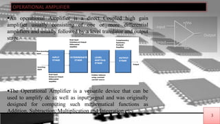
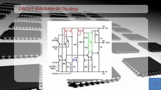
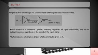
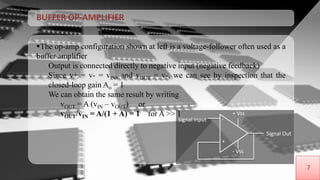
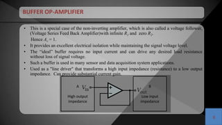
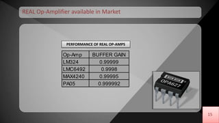
1
Buffer Op-Amplifier
I/P O/P
1
CONTENT
 Operational Amplifier
Buffer
Buffered Op-Amp
Basic Buffer Amplifier Circuit
C-MOS Buffers Circuits
Applications
2
2
OPERATIONAL AMPLIFIER
An operational Amplifier is a direct Coupled high gain
amplifier usually consisting of one or more differential
amplifiers and usually followed by a level translator and output
stage.
The Operational Amplifier is a versatile device that can be
used to amplify dc as well as input signal and was originally
designed for computing such mathematical functions as
Addition, Subtraction, Multiplication and Integration etc.
3
3
- input
+ input
-
+
+ Vss
- Vss
Output
CIRCUIT DIAGRAM OF Op-Amp
4
4
INVERTING & NON-INVERTING OP-AMPLIFIER
Vout = - Vin(Rf/Rin) Vout = Vin(1+Rf/Rin)
INVERTING NON-INVERTING
5
5
In this circuit the input signal is
amplified by gain A and also inverted.
In this circuit the input signal is
amplified by gain A and is in phase with
input signal.
6
6
BUFFER
Digital Buffer is nothing a but Even numbers of NOT gates cascade Connected.
I/P O/P
(Same as Input)Invert of I/P
Ideal buffer has a properties :perfect linearity, regardless of signal amplitudes; and instant
output response, regardless of the speed of the input signal
Buffer is device which gives o/p as what ever input is given to it.
BUFFER OP-AMPLIFIER
7
7
signal input -
+
+ Vss
Signal Out
- Vss
The op-amp configuration shown at left is a voltage-follower often used as a
buffer amplifier
Output is connected directly to negative input (negative feedback)
Since v+ = v- = vIN, and vOUT = v-, we can see by inspection that the
closed-loop gain Ao = 1
We can obtain the same result by writing
vOUT = A (vIN – vOUT) or
vOUT/vIN = A/(1 + A) = 1 for A >> 1
8
88
• This is a special case of the non-inverting amplifier, which is also called a voltage follower,
(Voltage Series Feed Back Amplifier)with infinite R1 and zero R2.
Hence Av = 1.
• It provides an excellent electrical isolation while maintaining the signal voltage level.
• The “ideal” buffer requires no input current and can drive any desired load resistance
without loss of signal voltage.
• Such a buffer is used in many sensor and data acquisition system applications.
• Used as a "line driver" that transforms a high input impedance (resistance) to a low output
impedance. Can provide substantial current gain.
BUFFER OP-AMPLIFIER
A
High output
impedance
B
Low input
impedance
9
9
0inOOis VAIRIRV:KVL
0inOO VAIRoutV-:KVL
IRV iin:VARIABLEGCONTROLLIN
iOO
is
out
RAR
RV
V
1
1
SOLVING
1
S
out
O
V
V
A
CIRCUIT AND MODEL FOR UNITY GAIN BUFFER
10
10
TRANSFER CURVE
A typical voltage-follower transfer curve is shown for VPOS = +15V and
VNEG = -10V
For vIN between –10 and +15 volts, vOUT = vIN
If vIN exceeds +15V, the output saturates at VPOS
If vIN < -10V, the output saturates at VNEG
Since input current is zero giving zero input power, the voltage follower can
provide a large power gain.
BASIC BUFFER CIRCUIT
11
Vout(Inverted)
Vout(Non-Inverted)
-
+
+
-
+5
-5
R2
R1
R3
Vin
Vin
Gnd
-5
4
4
7
6
6
5
8
1
5
8
1
2
3
3
2
12
C-MOS Buffer Circuit
13
C-MOS op-amp with low impedance driving capability
14
Buffer StageDifferential Amplifier Stages
Low output resistance C-MOS op-amp Suitable for Driving Resistive Captive Load
15
15
PERFORMANCE OF REAL OP-AMPS
Op-Amp BUFFER GAIN
LM324 0.99999
LMC6492 0.9998
MAX4240 0.99995
PA05 0.999992
REAL Op-Amplifier available in Market
16
16
References
 “Allen and Holberg “ - “CMOS Analog Circuit Design”
17

Buffer op amplifier

  • 1.
  • 2.
    CONTENT  Operational Amplifier Buffer BufferedOp-Amp Basic Buffer Amplifier Circuit C-MOS Buffers Circuits Applications 2 2
  • 3.
    OPERATIONAL AMPLIFIER An operationalAmplifier is a direct Coupled high gain amplifier usually consisting of one or more differential amplifiers and usually followed by a level translator and output stage. The Operational Amplifier is a versatile device that can be used to amplify dc as well as input signal and was originally designed for computing such mathematical functions as Addition, Subtraction, Multiplication and Integration etc. 3 3 - input + input - + + Vss - Vss Output
  • 4.
  • 5.
    INVERTING & NON-INVERTINGOP-AMPLIFIER Vout = - Vin(Rf/Rin) Vout = Vin(1+Rf/Rin) INVERTING NON-INVERTING 5 5 In this circuit the input signal is amplified by gain A and also inverted. In this circuit the input signal is amplified by gain A and is in phase with input signal.
  • 6.
    6 6 BUFFER Digital Buffer isnothing a but Even numbers of NOT gates cascade Connected. I/P O/P (Same as Input)Invert of I/P Ideal buffer has a properties :perfect linearity, regardless of signal amplitudes; and instant output response, regardless of the speed of the input signal Buffer is device which gives o/p as what ever input is given to it.
  • 7.
    BUFFER OP-AMPLIFIER 7 7 signal input- + + Vss Signal Out - Vss The op-amp configuration shown at left is a voltage-follower often used as a buffer amplifier Output is connected directly to negative input (negative feedback) Since v+ = v- = vIN, and vOUT = v-, we can see by inspection that the closed-loop gain Ao = 1 We can obtain the same result by writing vOUT = A (vIN – vOUT) or vOUT/vIN = A/(1 + A) = 1 for A >> 1
  • 8.
    8 88 • This isa special case of the non-inverting amplifier, which is also called a voltage follower, (Voltage Series Feed Back Amplifier)with infinite R1 and zero R2. Hence Av = 1. • It provides an excellent electrical isolation while maintaining the signal voltage level. • The “ideal” buffer requires no input current and can drive any desired load resistance without loss of signal voltage. • Such a buffer is used in many sensor and data acquisition system applications. • Used as a "line driver" that transforms a high input impedance (resistance) to a low output impedance. Can provide substantial current gain. BUFFER OP-AMPLIFIER A High output impedance B Low input impedance
  • 9.
    9 9 0inOOis VAIRIRV:KVL 0inOO VAIRoutV-:KVL IRViin:VARIABLEGCONTROLLIN iOO is out RAR RV V 1 1 SOLVING 1 S out O V V A CIRCUIT AND MODEL FOR UNITY GAIN BUFFER
  • 10.
    10 10 TRANSFER CURVE A typicalvoltage-follower transfer curve is shown for VPOS = +15V and VNEG = -10V For vIN between –10 and +15 volts, vOUT = vIN If vIN exceeds +15V, the output saturates at VPOS If vIN < -10V, the output saturates at VNEG Since input current is zero giving zero input power, the voltage follower can provide a large power gain.
  • 11.
  • 12.
  • 13.
    13 C-MOS op-amp withlow impedance driving capability
  • 14.
    14 Buffer StageDifferential AmplifierStages Low output resistance C-MOS op-amp Suitable for Driving Resistive Captive Load
  • 15.
    15 15 PERFORMANCE OF REALOP-AMPS Op-Amp BUFFER GAIN LM324 0.99999 LMC6492 0.9998 MAX4240 0.99995 PA05 0.999992 REAL Op-Amplifier available in Market
  • 16.
    16 16 References  “Allen andHolberg “ - “CMOS Analog Circuit Design”
  • 17.

Editor's Notes

  • #9 IdelVoltege series feedback amplifier has infitityRi and 0 output Ro and 1 gain.