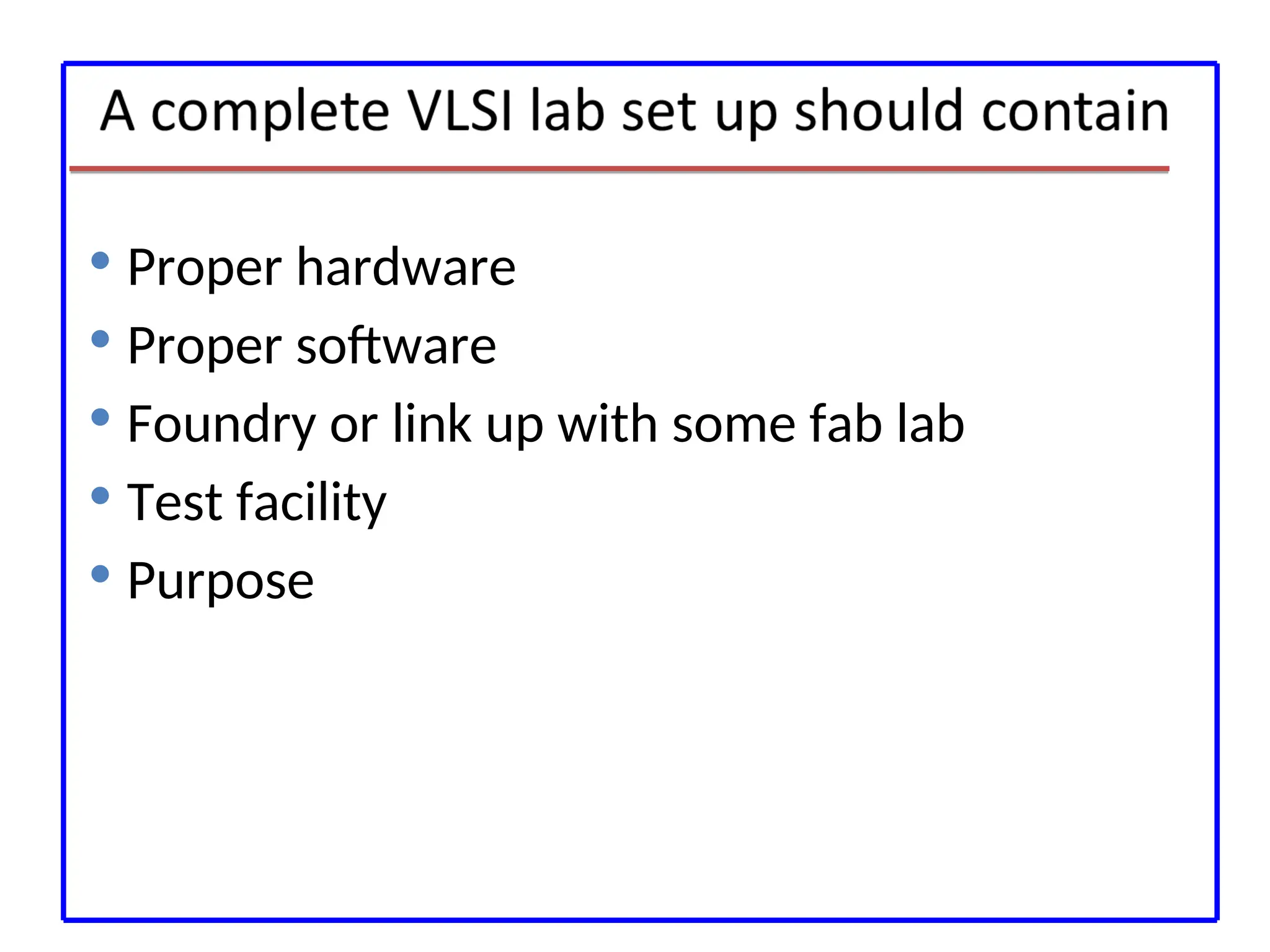
Proper hardware
Proper software
Foundry or link up with some fab lab
Test facility
Purpose
4.
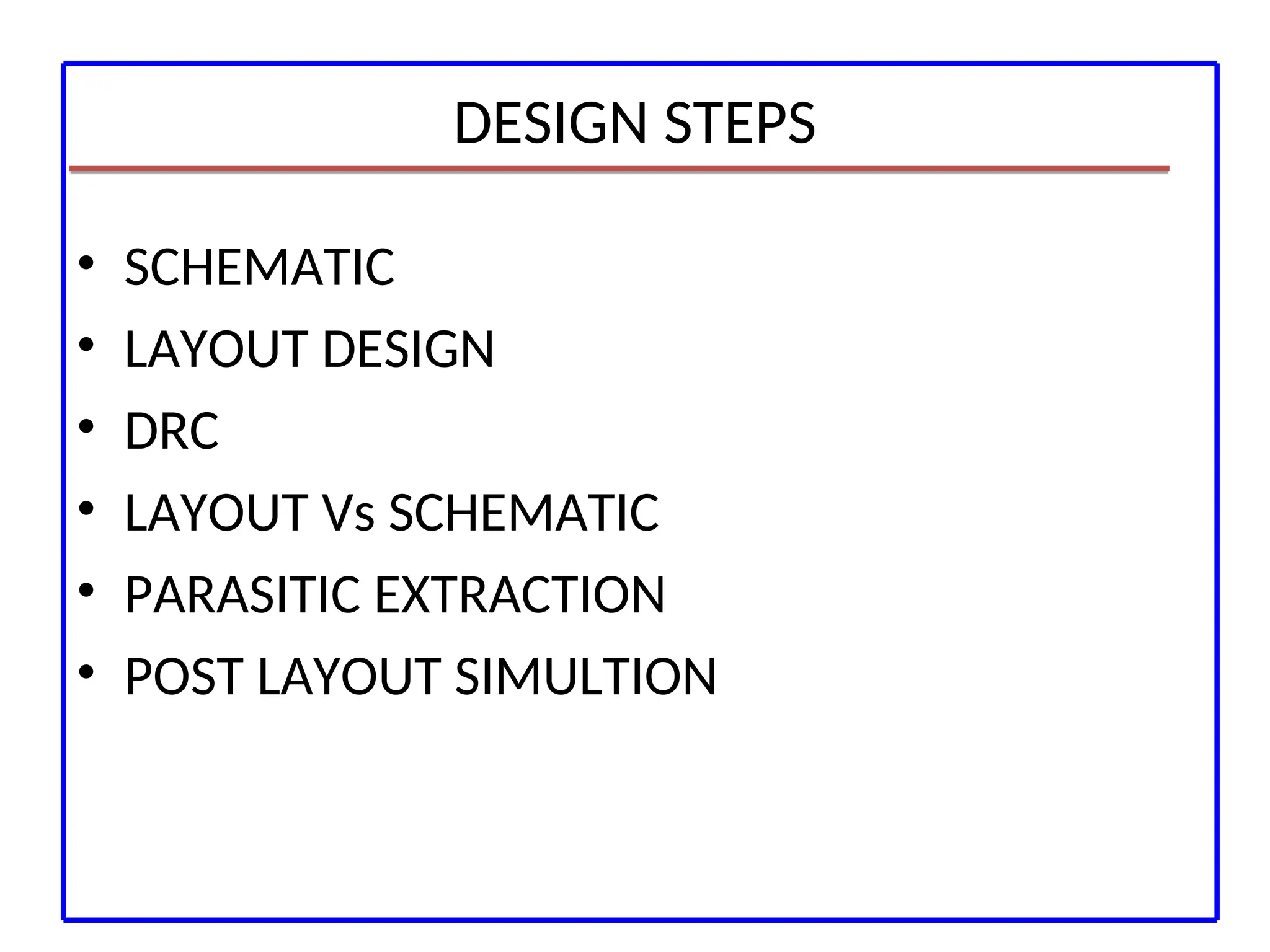
DESIGN STEPS
• SCHEMATIC
•LAYOUT DESIGN
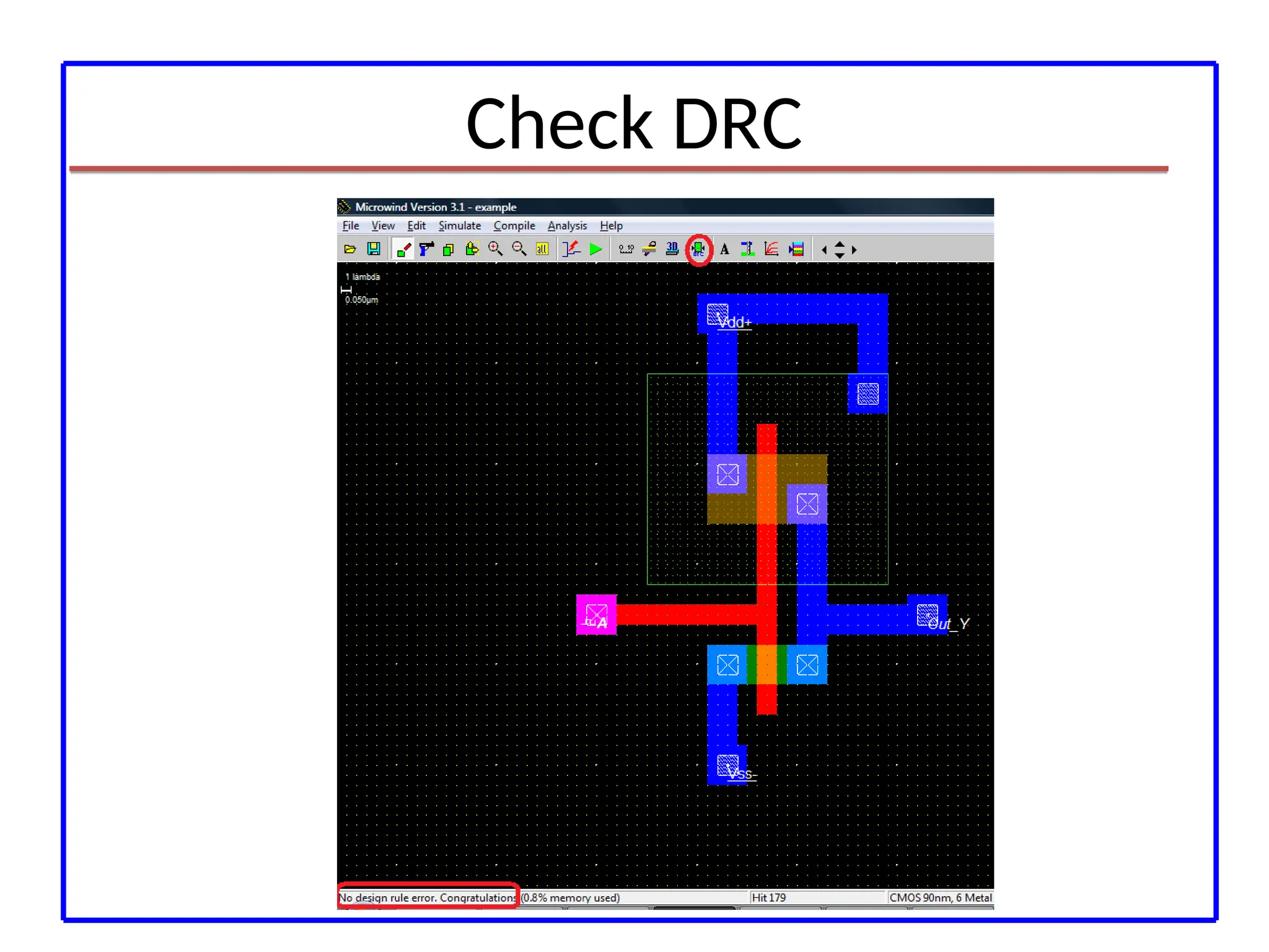
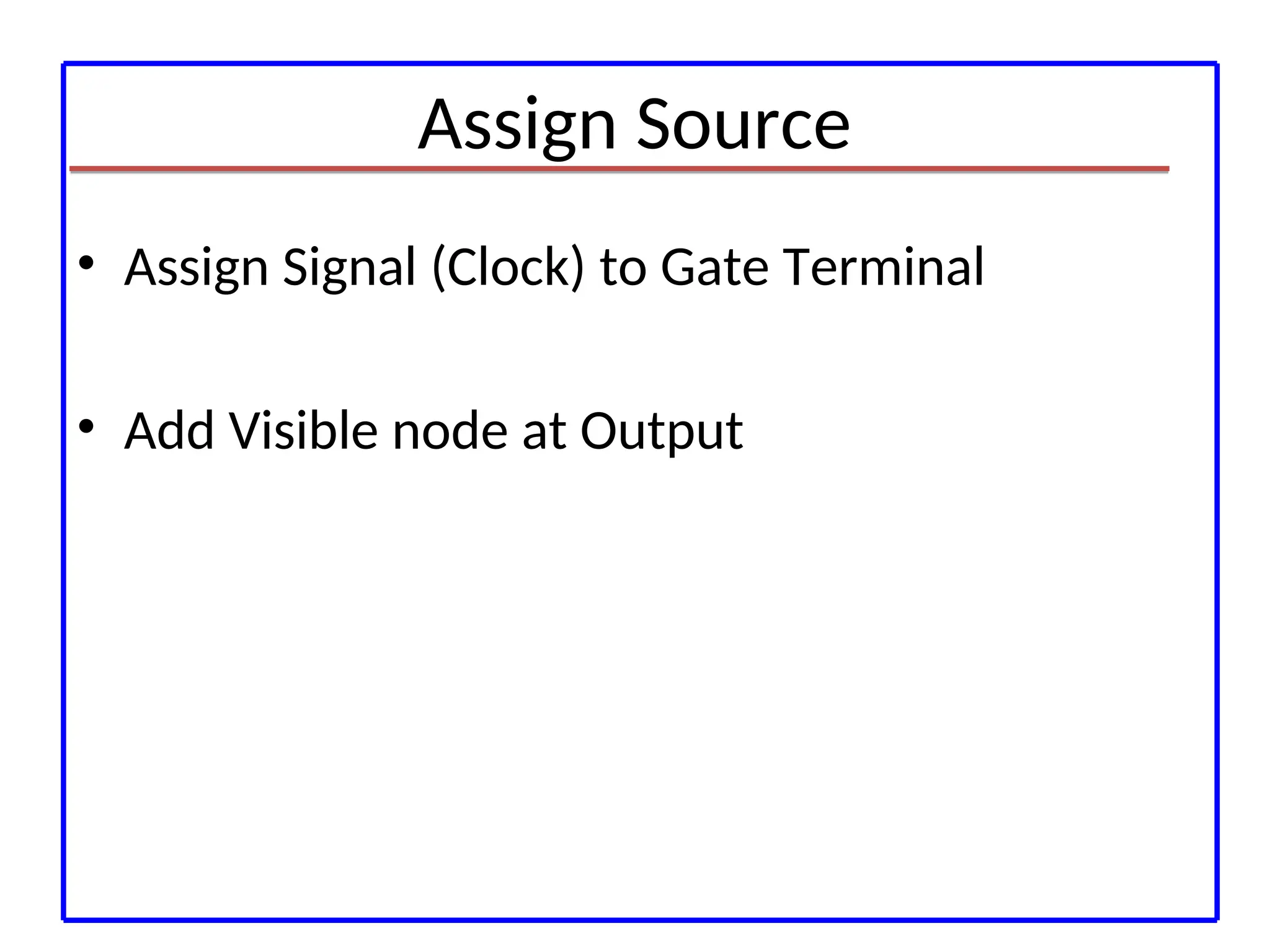
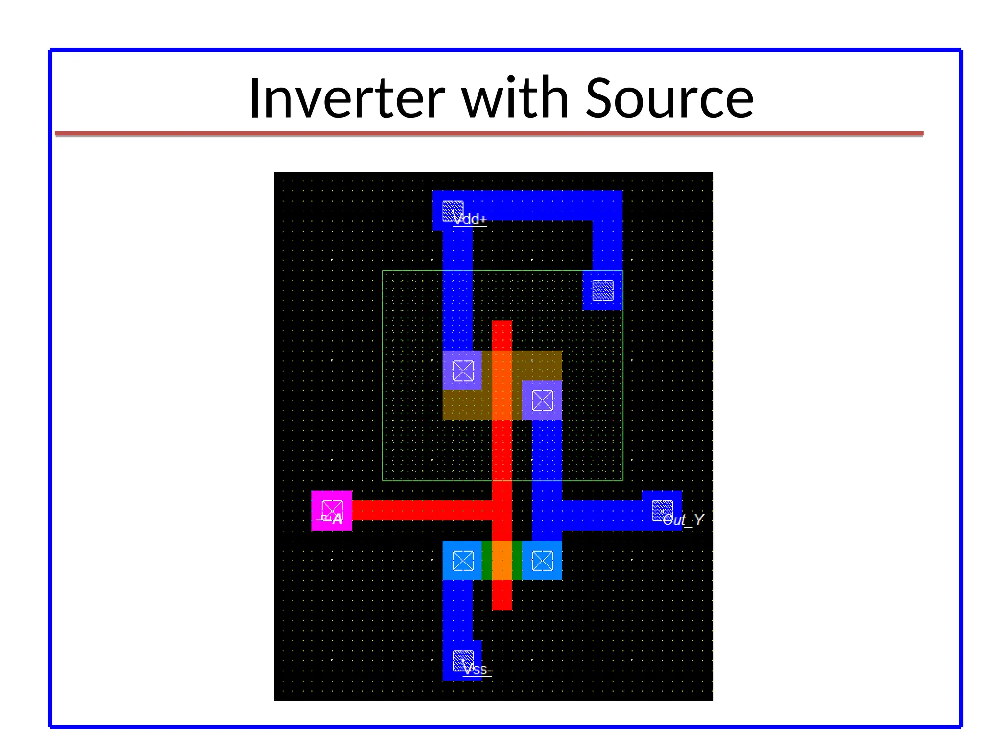
• DRC
• LAYOUT Vs SCHEMATIC
• PARASITIC EXTRACTION
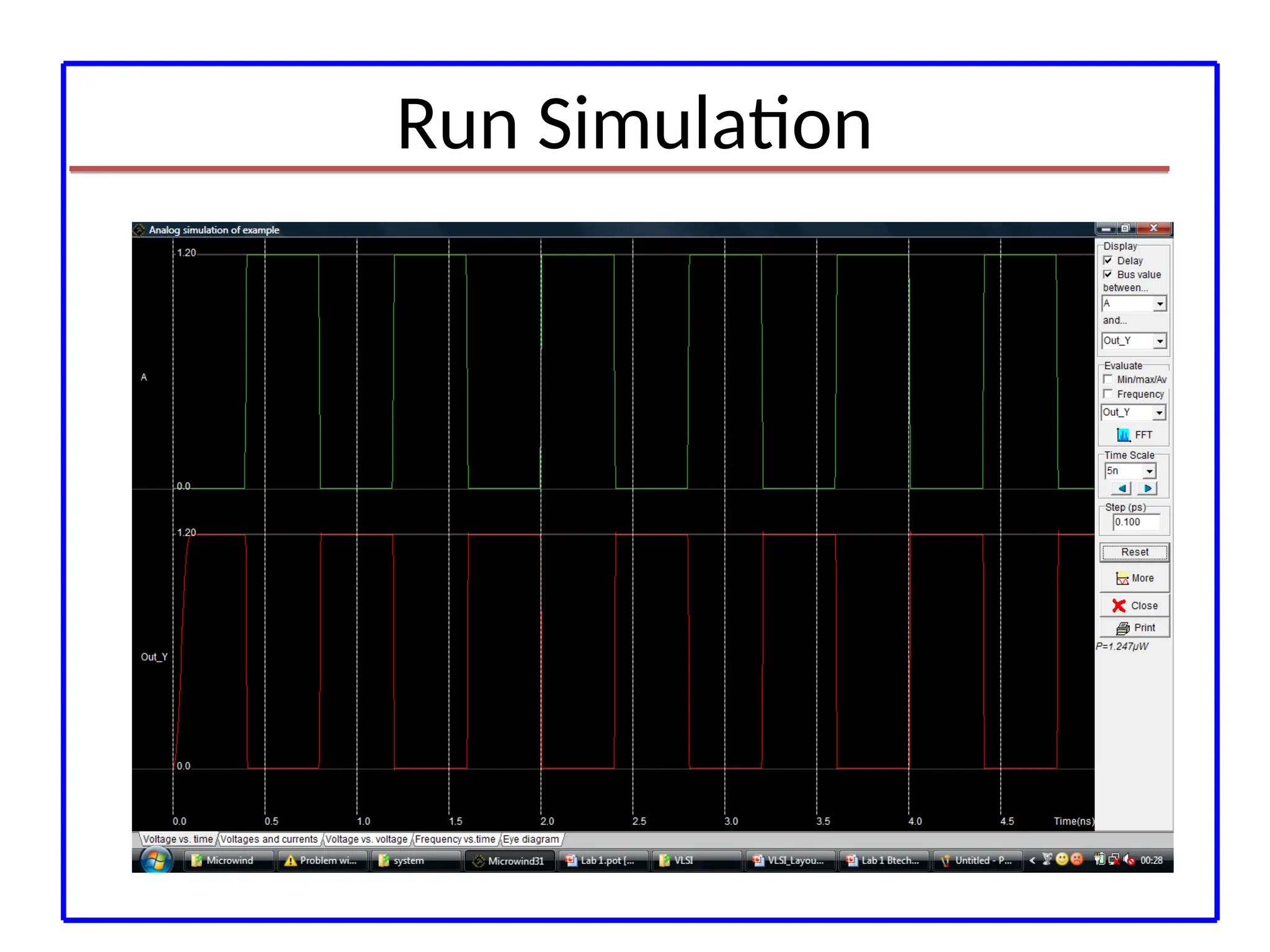
• POST LAYOUT SIMULTION
5.
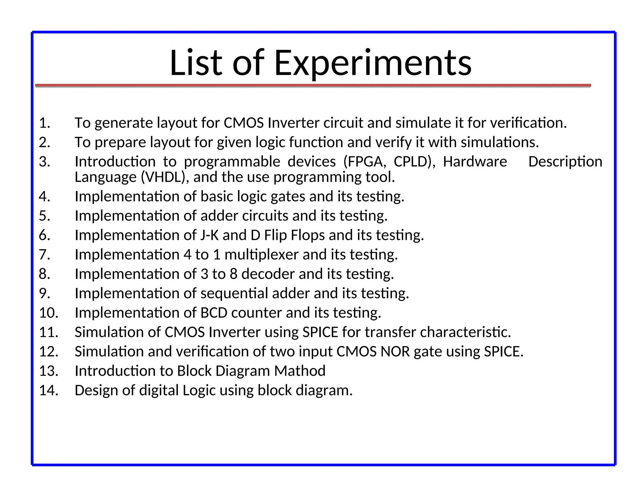
List of Experiments
1.To generate layout for CMOS Inverter circuit and simulate it for verification.
2. To prepare layout for given logic function and verify it with simulations.
3. Introduction to programmable devices (FPGA, CPLD), Hardware Description
Language (VHDL), and the use programming tool.
4. Implementation of basic logic gates and its testing.
5. Implementation of adder circuits and its testing.
6. Implementation of J-K and D Flip Flops and its testing.
7. Implementation 4 to 1 multiplexer and its testing.
8. Implementation of 3 to 8 decoder and its testing.
9. Implementation of sequential adder and its testing.
10. Implementation of BCD counter and its testing.
11. Simulation of CMOS Inverter using SPICE for transfer characteristic.
12. Simulation and verification of two input CMOS NOR gate using SPICE.
13. Introduction to Block Diagram Mathod
14. Design of digital Logic using block diagram.
6.
Project
• Mini Project:VHDL/Verilog based mini project
with emphasis on design and implementation
into the group of maximum 3 students.
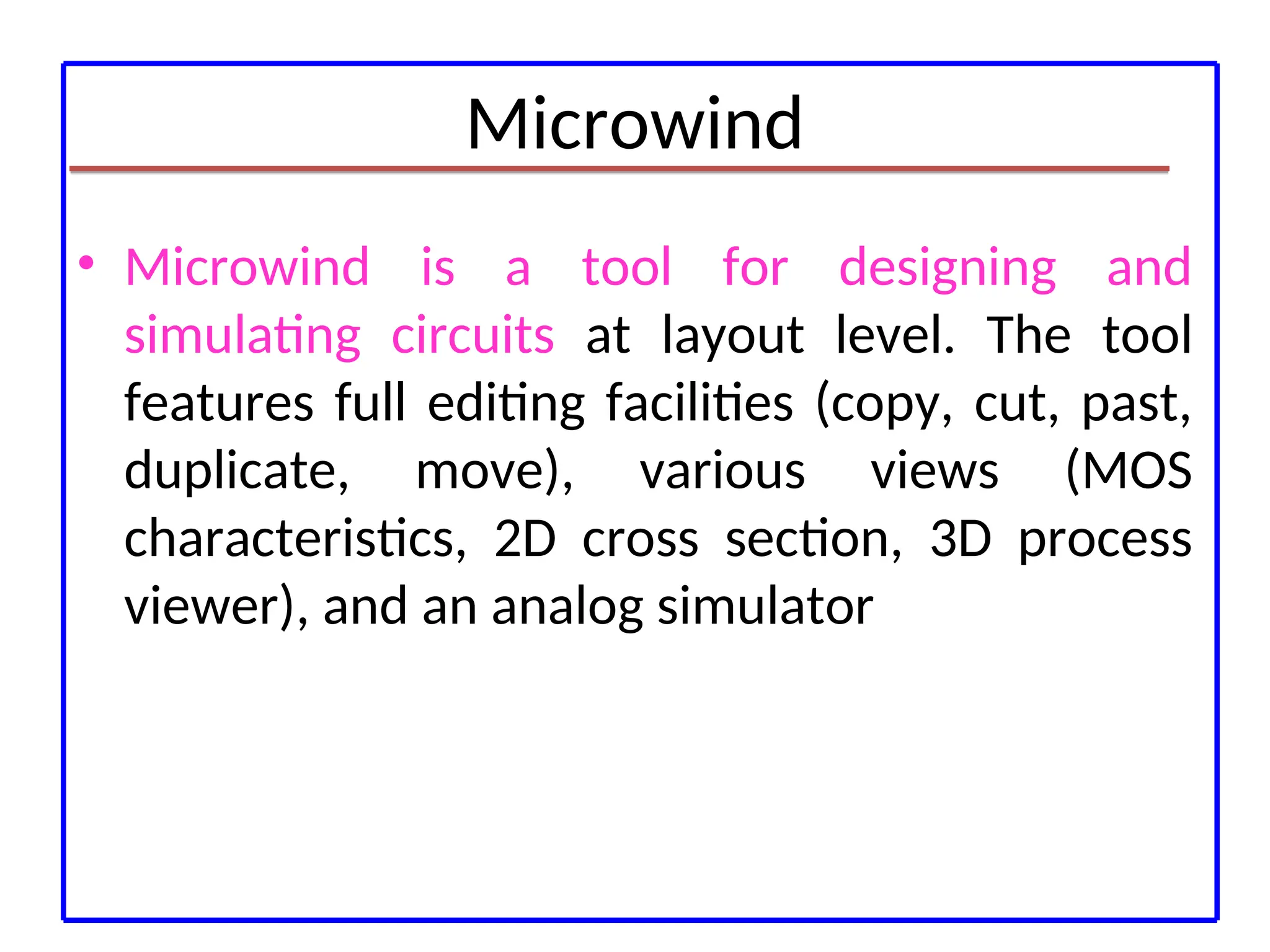
Microwind
• Microwind isa tool for designing and
simulating circuits at layout level. The tool
features full editing facilities (copy, cut, past,
duplicate, move), various views (MOS
characteristics, 2D cross section, 3D process
viewer), and an analog simulator
9.
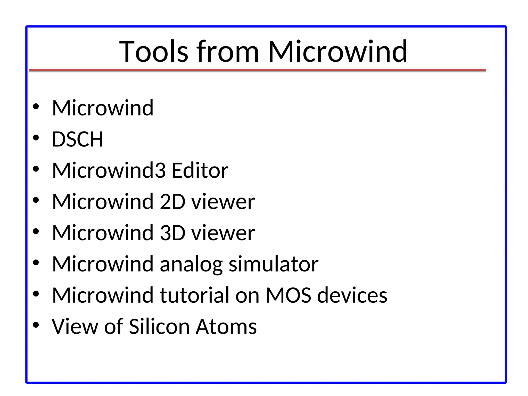
Tools from Microwind
•Microwind
• DSCH
• Microwind3 Editor
• Microwind 2D viewer
• Microwind 3D viewer
• Microwind analog simulator
• Microwind tutorial on MOS devices
• View of Silicon Atoms
10.
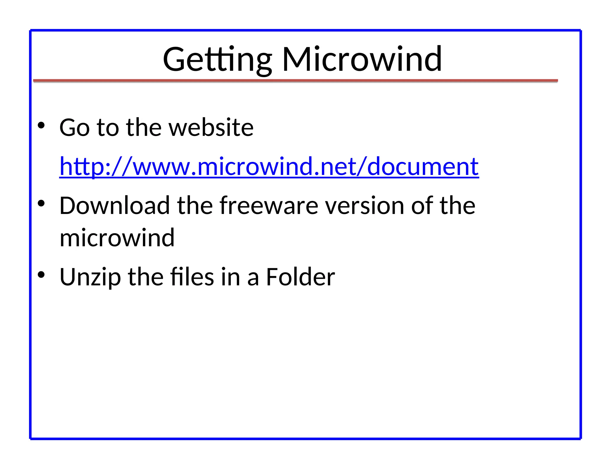
Getting Microwind
• Goto the website
http://www.microwind.net/document
• Download the freeware version of the
microwind
• Unzip the files in a Folder
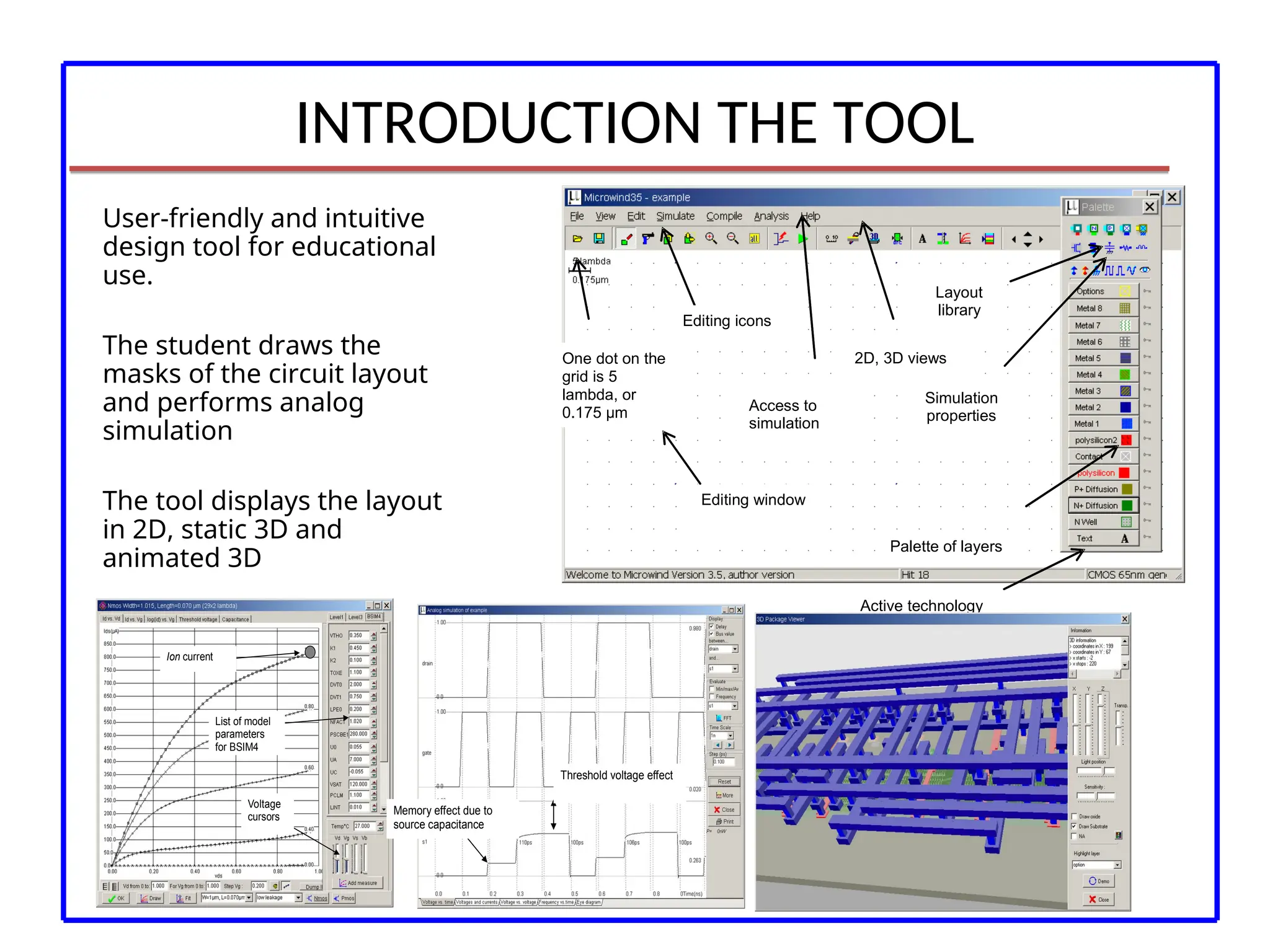
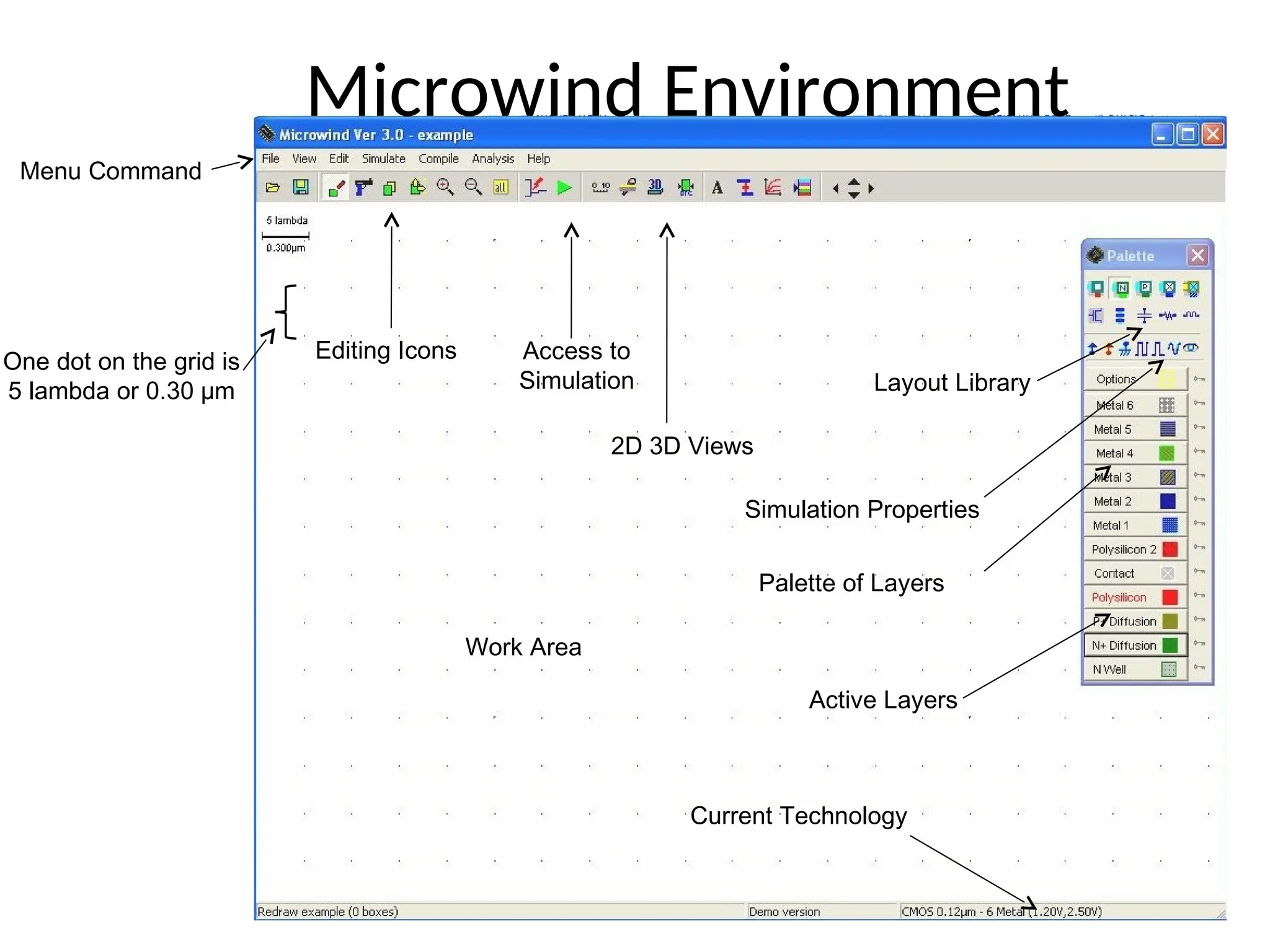
INTRODUCTION THE TOOL
User-friendlyand intuitive
design tool for educational
use.
The student draws the
masks of the circuit layout
and performs analog
simulation
The tool displays the layout
in 2D, static 3D and
animated 3D
Editing window
One dot on the
grid is 5
lambda, or
0.175 µm
Editing icons
Access to
simulation
2D, 3D views
Simulation
properties
Layout
library
Active technology
Palette of layers
Ion current
Voltage
cursors
List of model
parameters
for BSIM4
Memory effect due to
source capacitance
Threshold voltage effect
13.
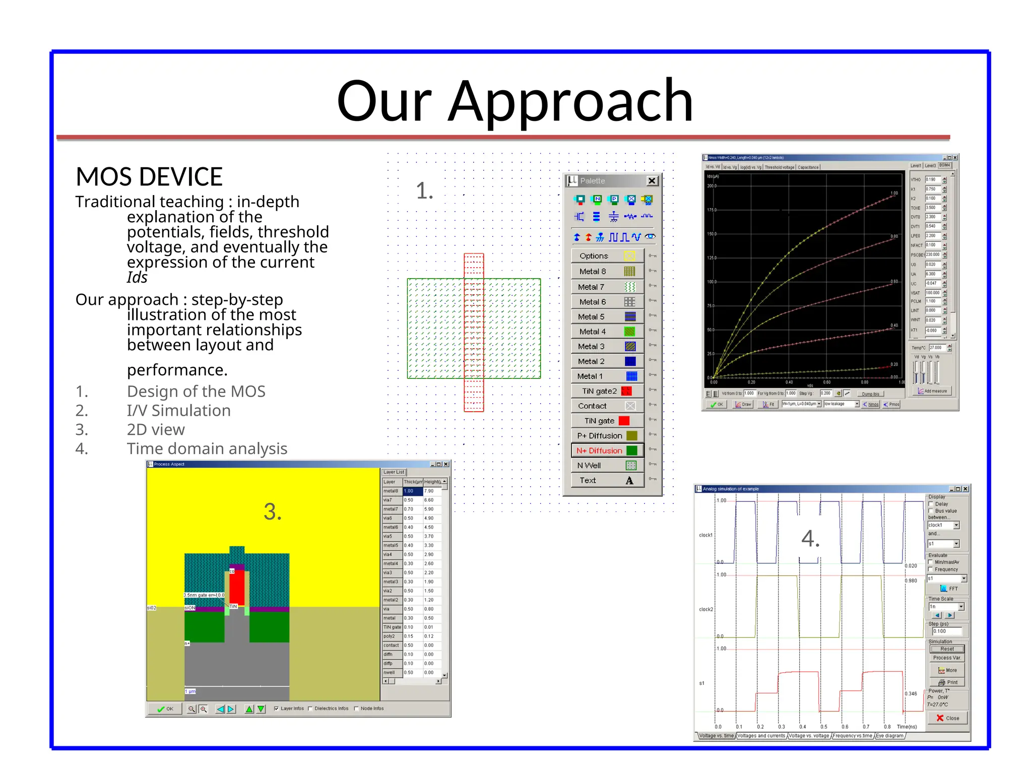
Our Approach
1.
2.
3.
4.
MOS DEVICE
Traditionalteaching : in-depth
explanation of the
potentials, fields, threshold
voltage, and eventually the
expression of the current
Ids
Our approach : step-by-step
illustration of the most
important relationships
between layout and
performance.
1. Design of the MOS
2. I/V Simulation
3. 2D view
4. Time domain analysis
14.
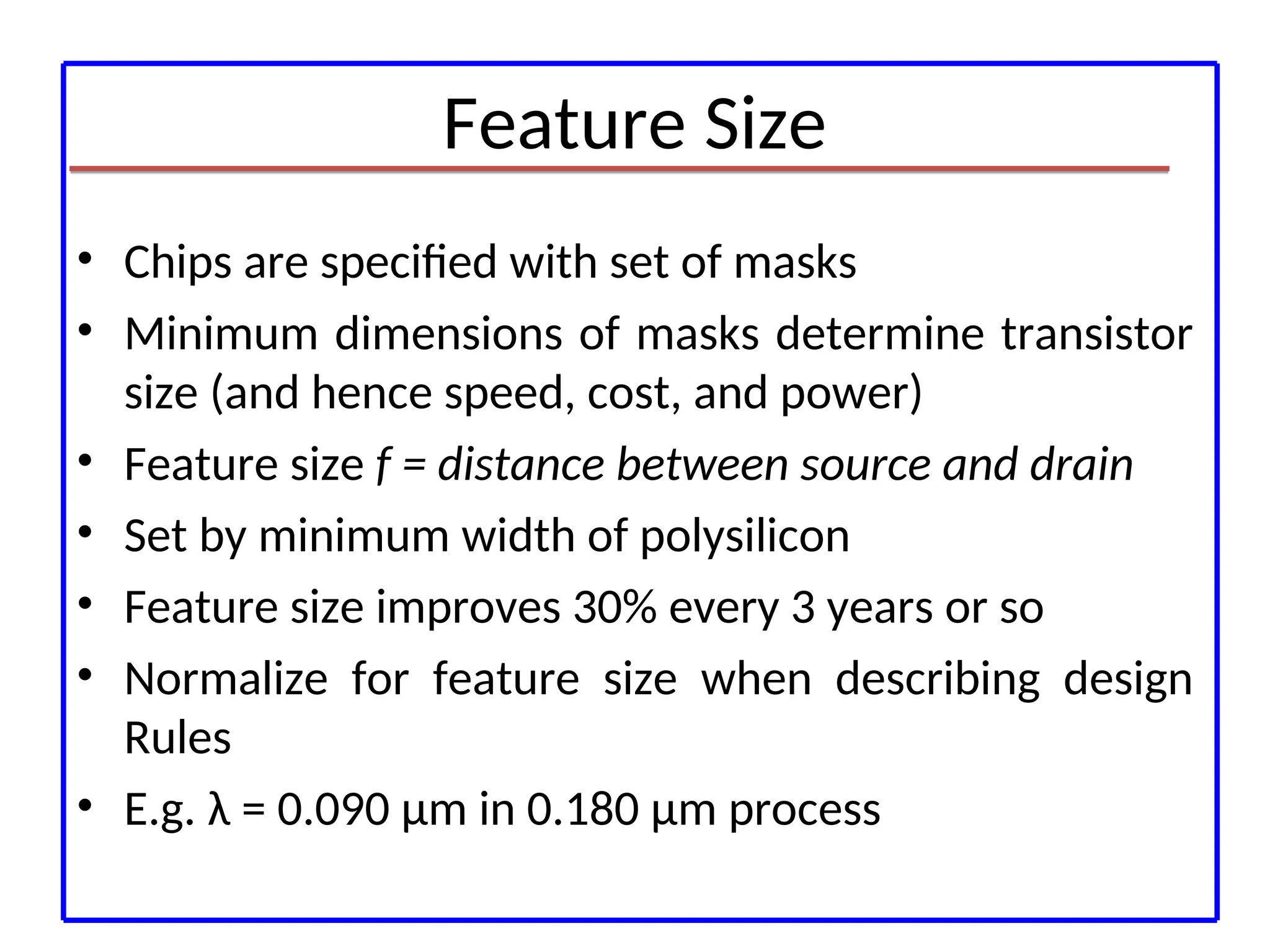
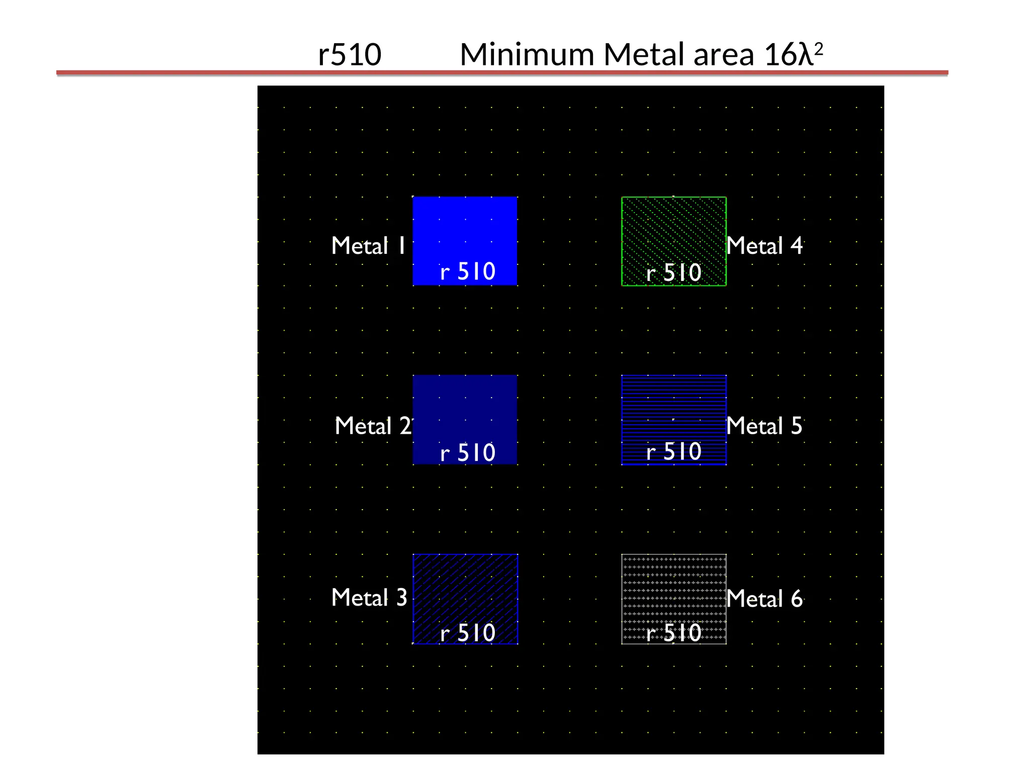
Feature Size
• Chipsare specified with set of masks
• Minimum dimensions of masks determine transistor
size (and hence speed, cost, and power)
• Feature size f = distance between source and drain
• Set by minimum width of polysilicon
• Feature size improves 30% every 3 years or so
• Normalize for feature size when describing design
Rules
• E.g. λ = 0.090 μm in 0.180 μm process
15.
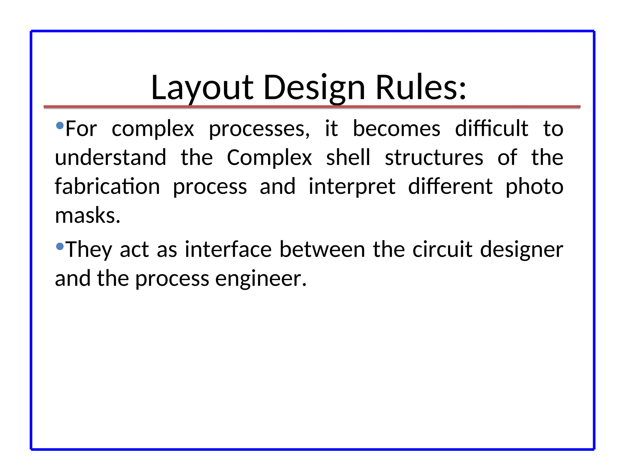
Layout Design Rules:
Forcomplex processes, it becomes difficult to
understand the Complex shell structures of the
fabrication process and interpret different photo
masks.
They act as interface between the circuit designer
and the process engineer.
16.
Editing Icons Accessto
Simulation
2D 3D Views
Layout Library
Simulation Properties
Palette of Layers
Active Layers
Current Technology
Work Area
One dot on the grid is
5 lambda or 0.30 µm
Menu Command
Microwind Environment
17.
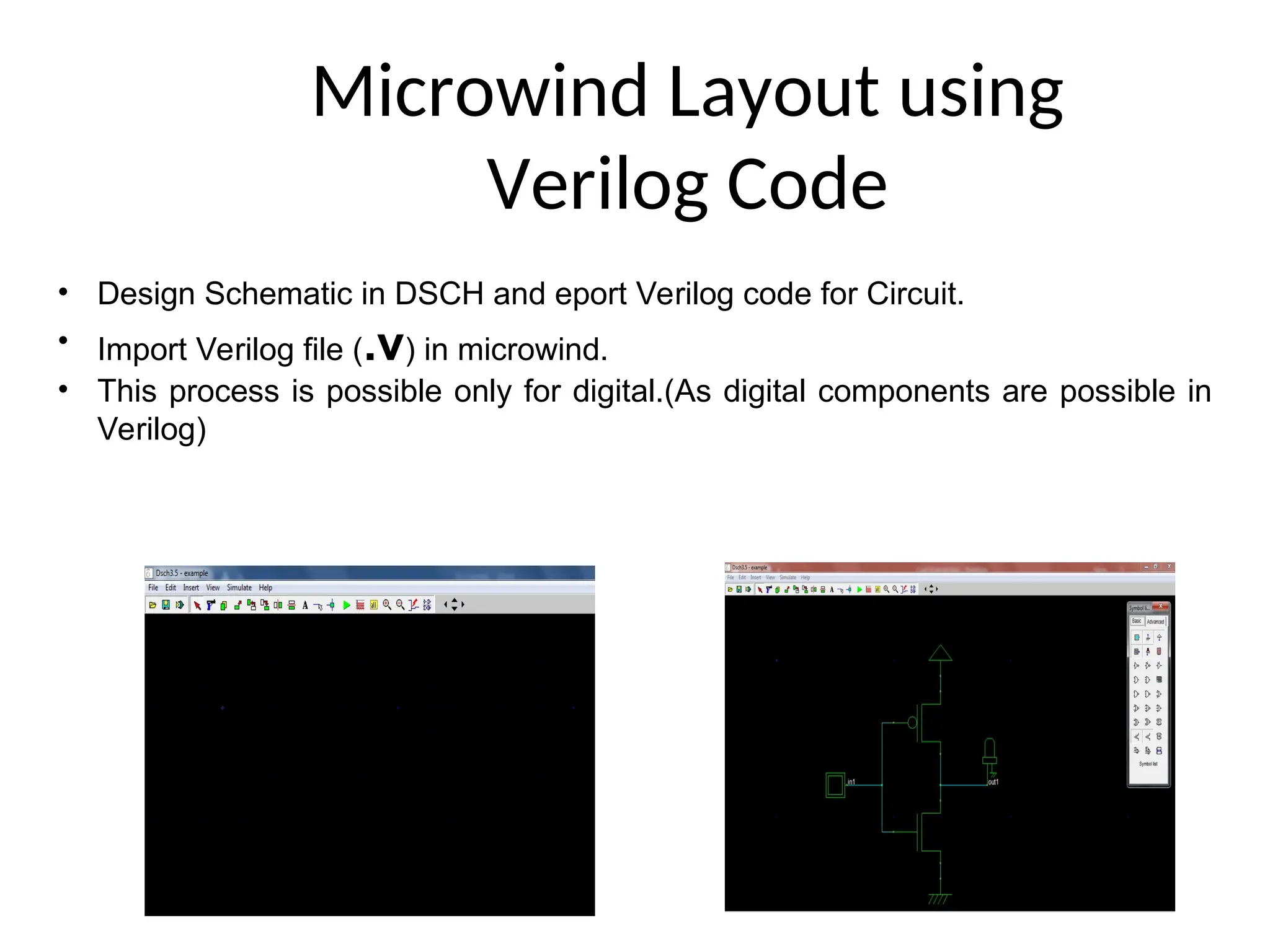
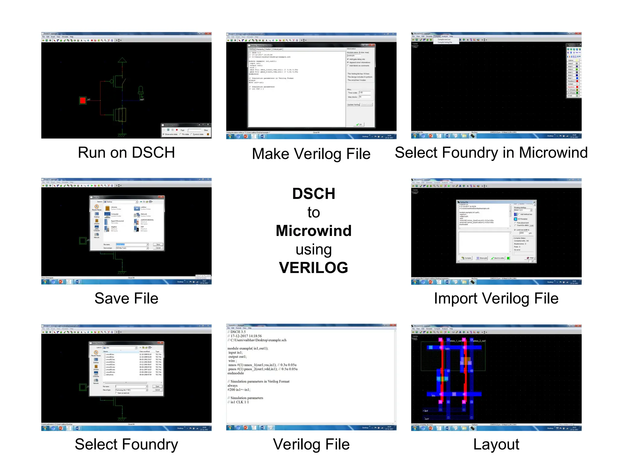
Microwind Layout using
VerilogCode
• Design Schematic in DSCH and eport Verilog code for Circuit.
• Import Verilog file (.v) in microwind.
• This process is possible only for digital.(As digital components are possible in
Verilog)
18.
Run on DSCH
SaveFile
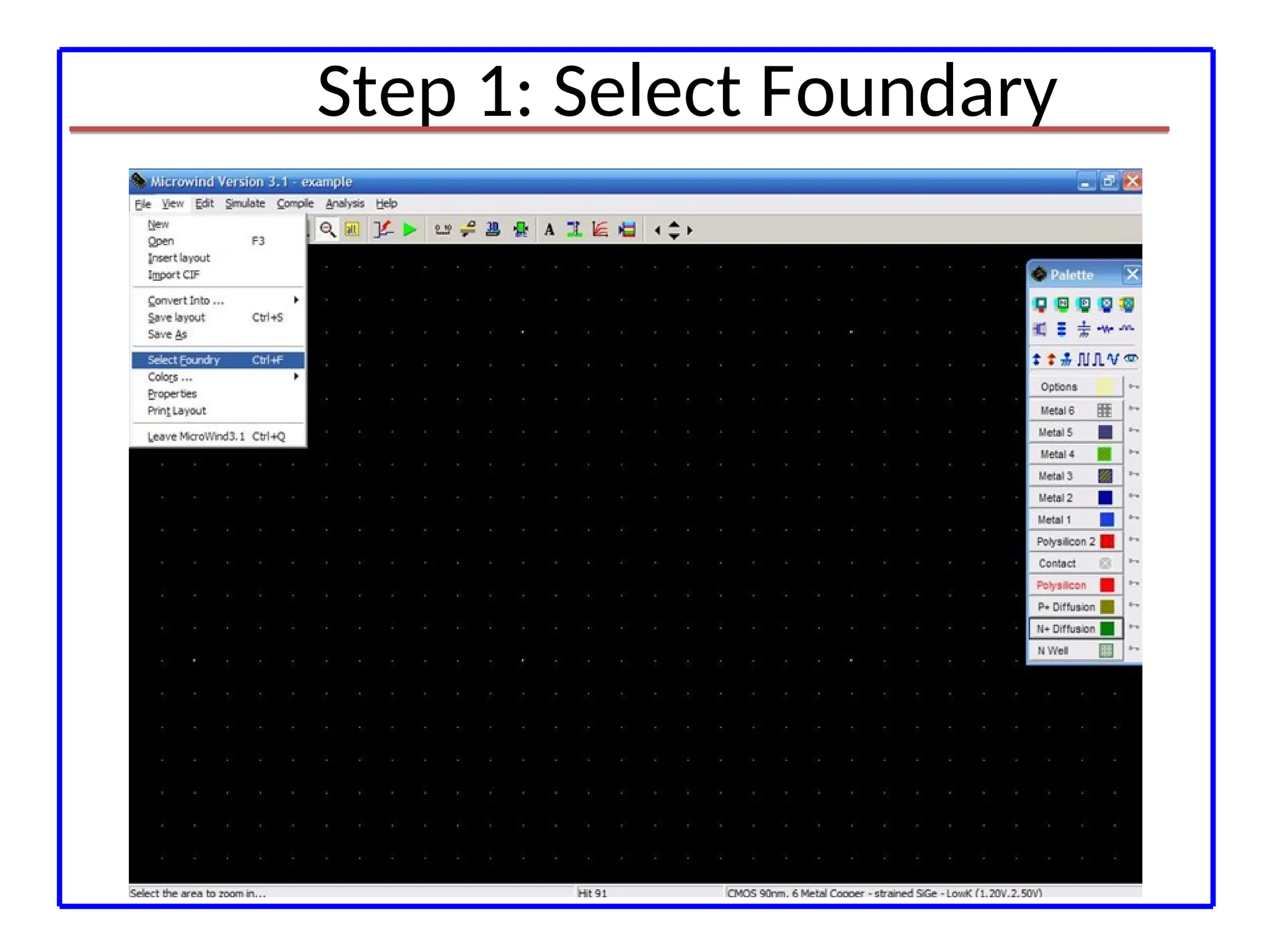
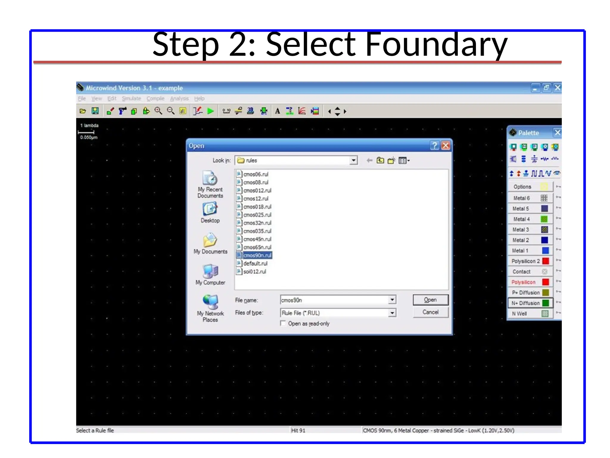
Select Foundry
Make Verilog File
Import Verilog File
Layout
Verilog File
Select Foundry in Microwind
DSCH
to
Microwind
using
VERILOG
19.
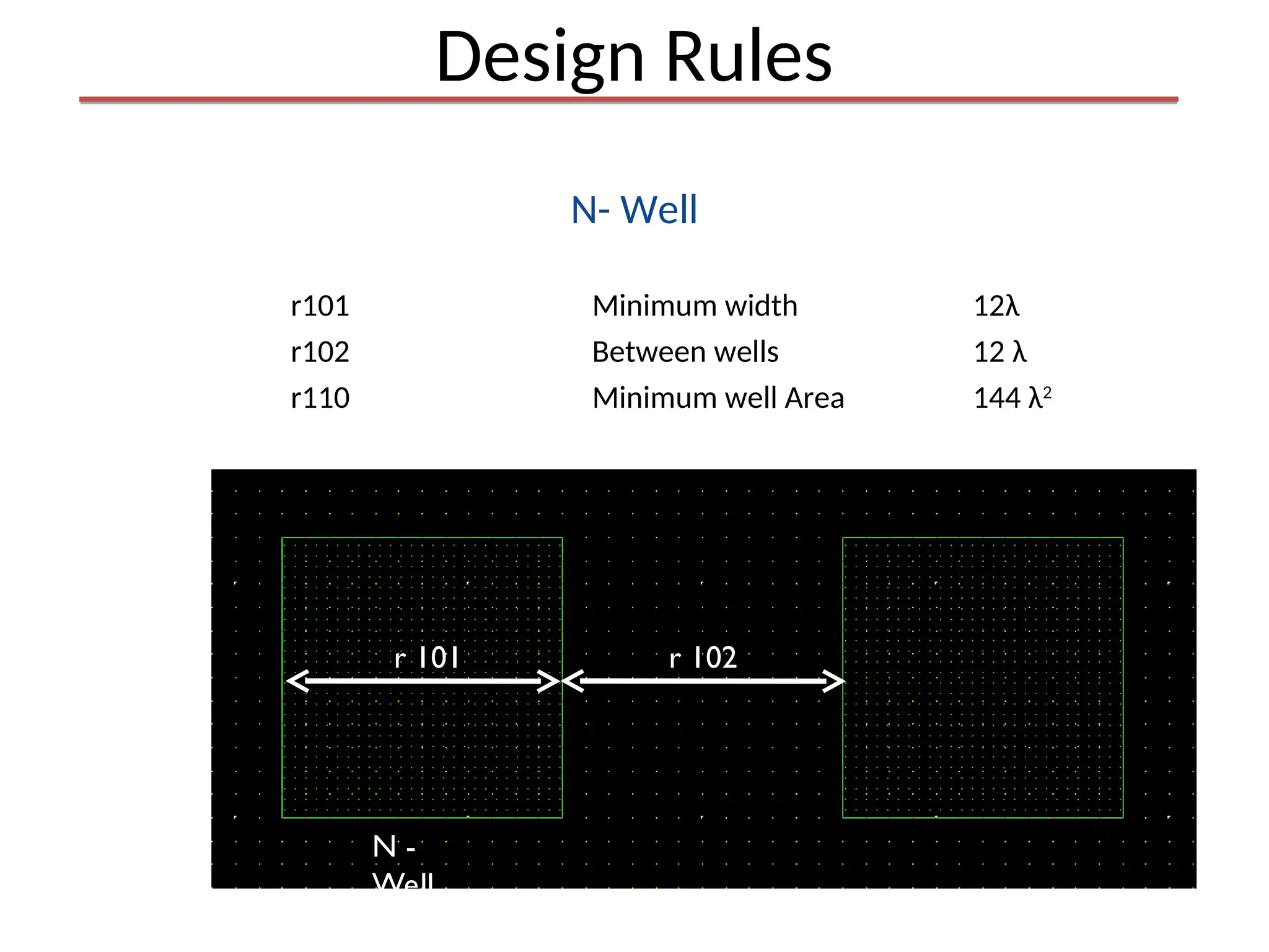
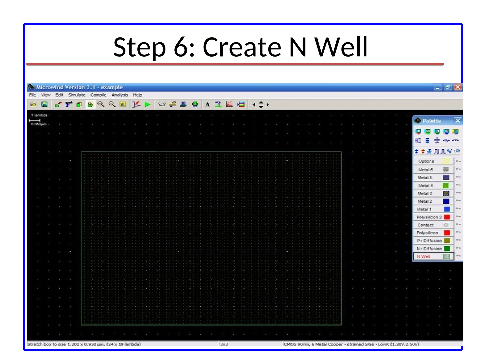
Design Rules
N- Well
r101Minimum width 12λ
r102 Between wells 12 λ
r110 Minimum well Area 144 λ2
r 102
r 101
N -
Well
20.
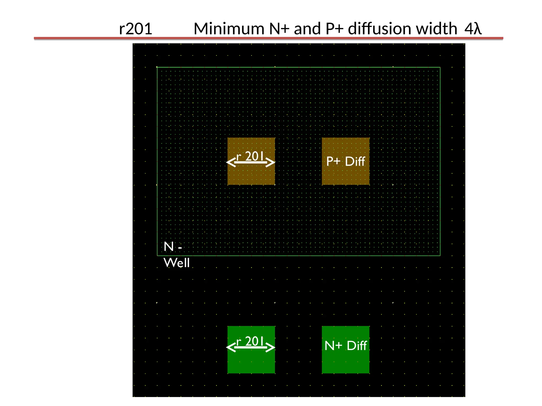
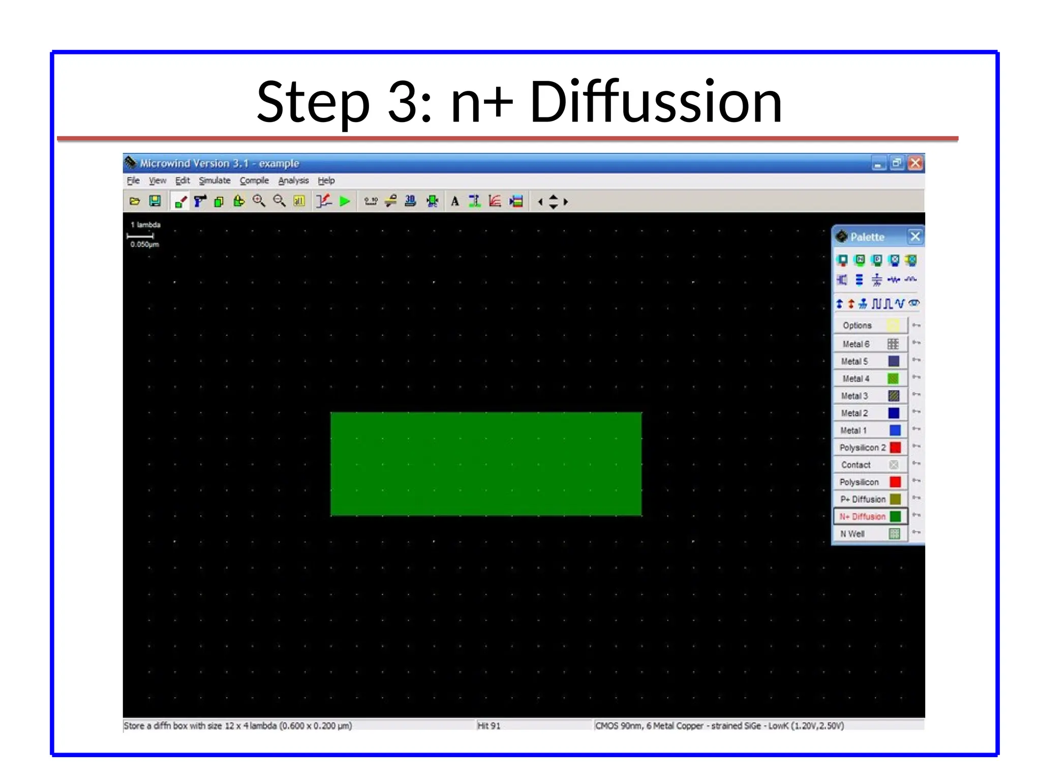
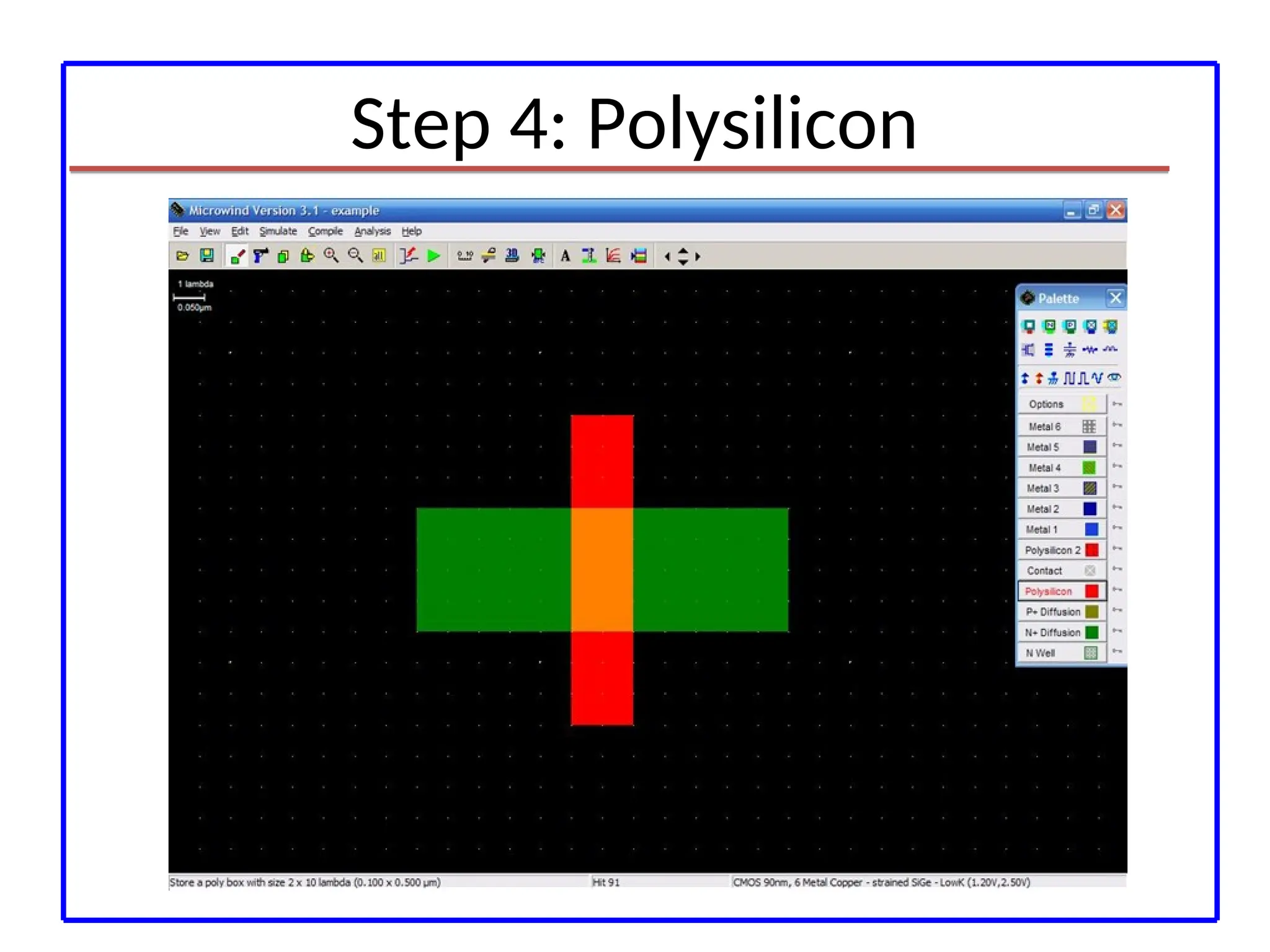
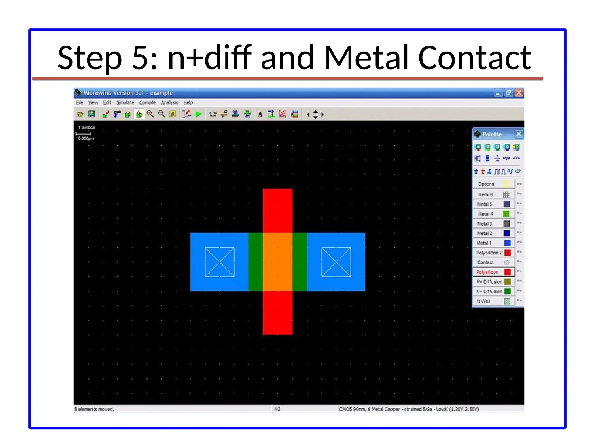
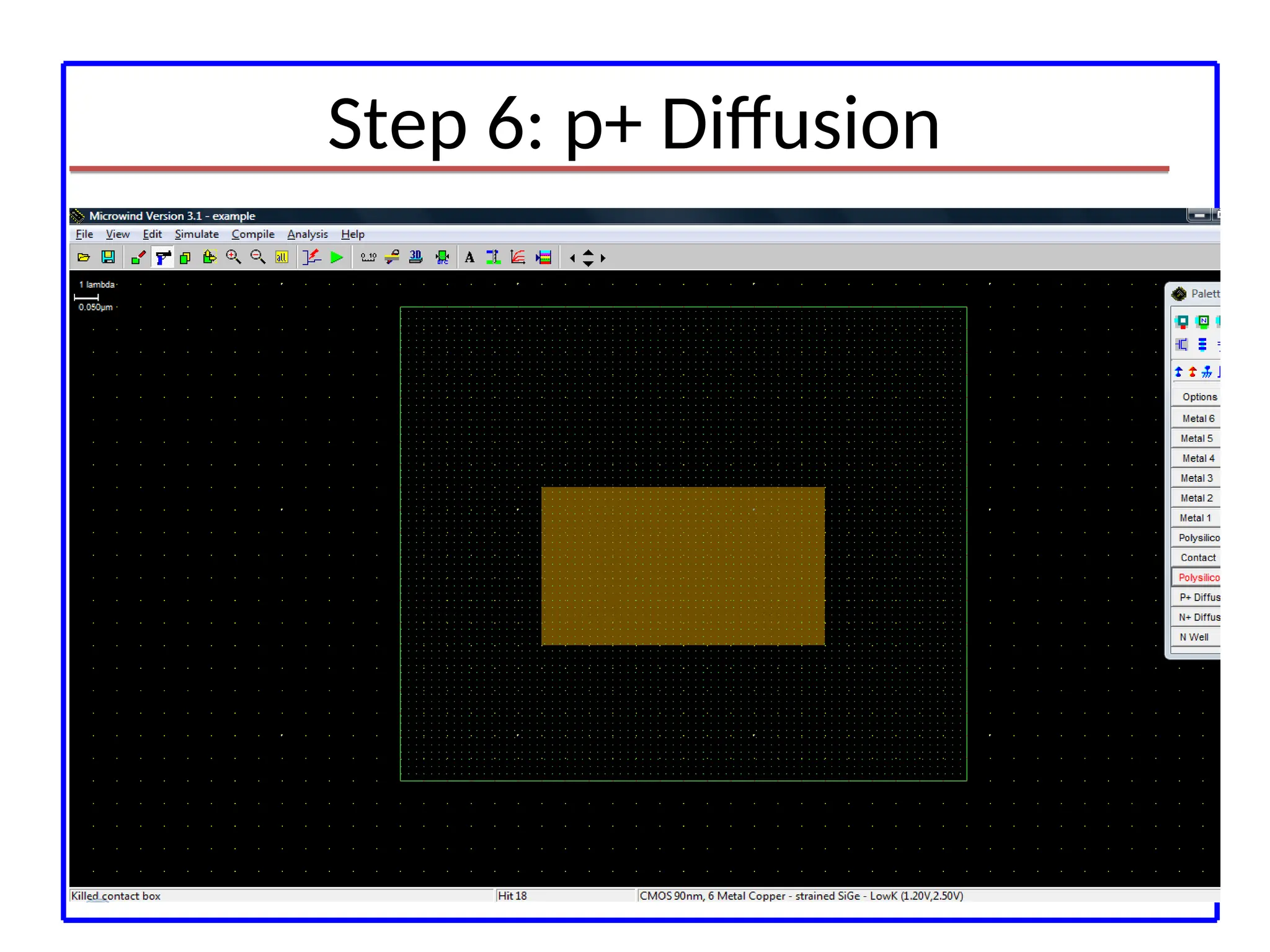
r201 Minimum N+and P+ diffusion width 4λ
r 201
r 201
N -
Well
P+ Diff
N+ Diff
21.
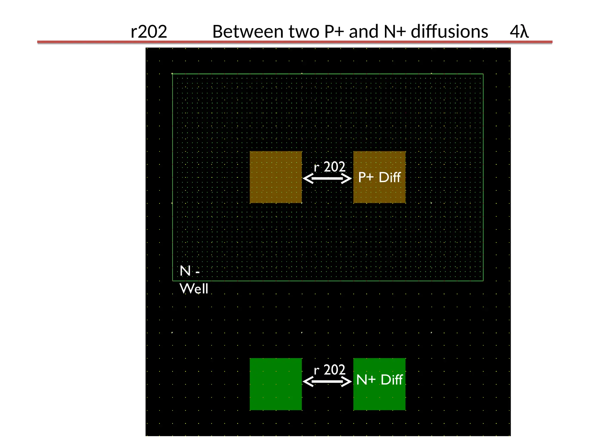
r202 Between twoP+ and N+ diffusions 4λ
N -
Well
P+ Diff
N+ Diff
r 202
r 202
22.
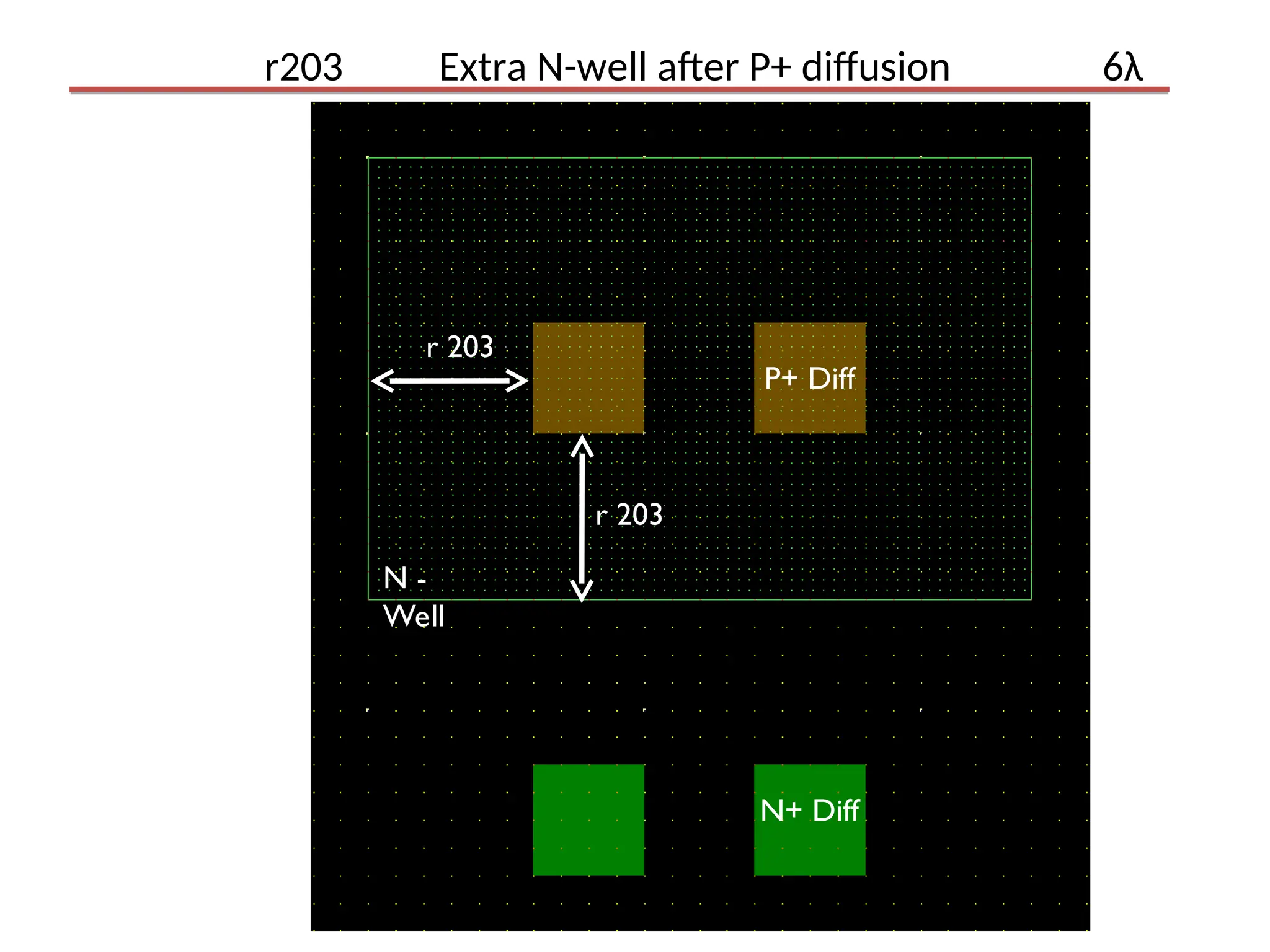
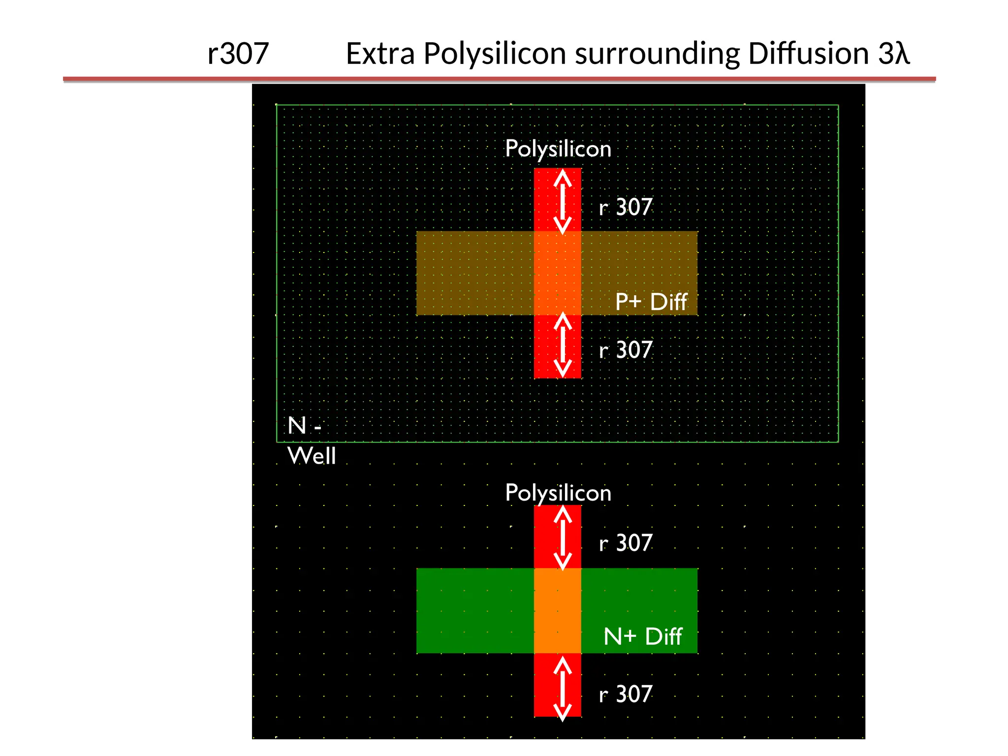
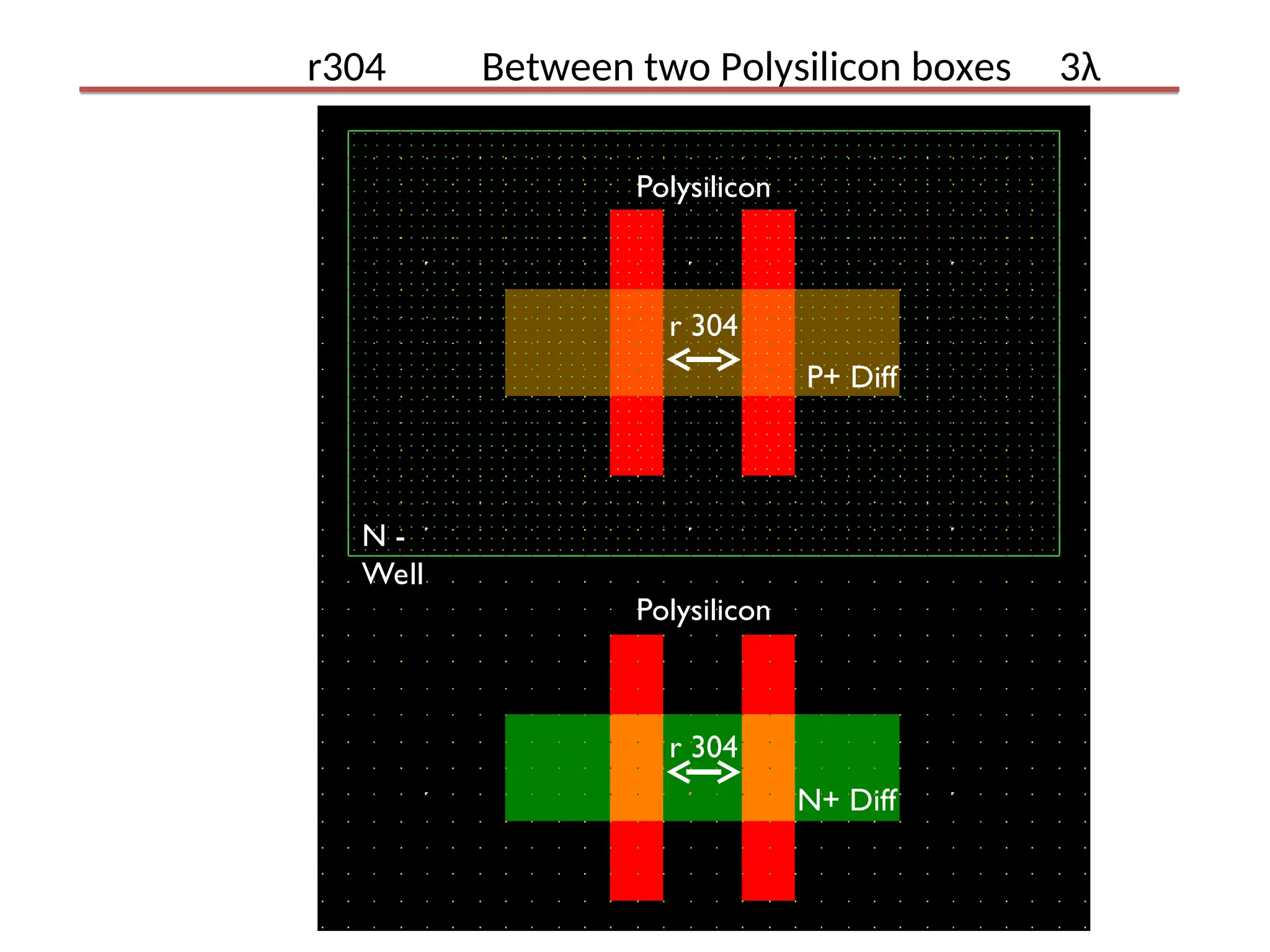
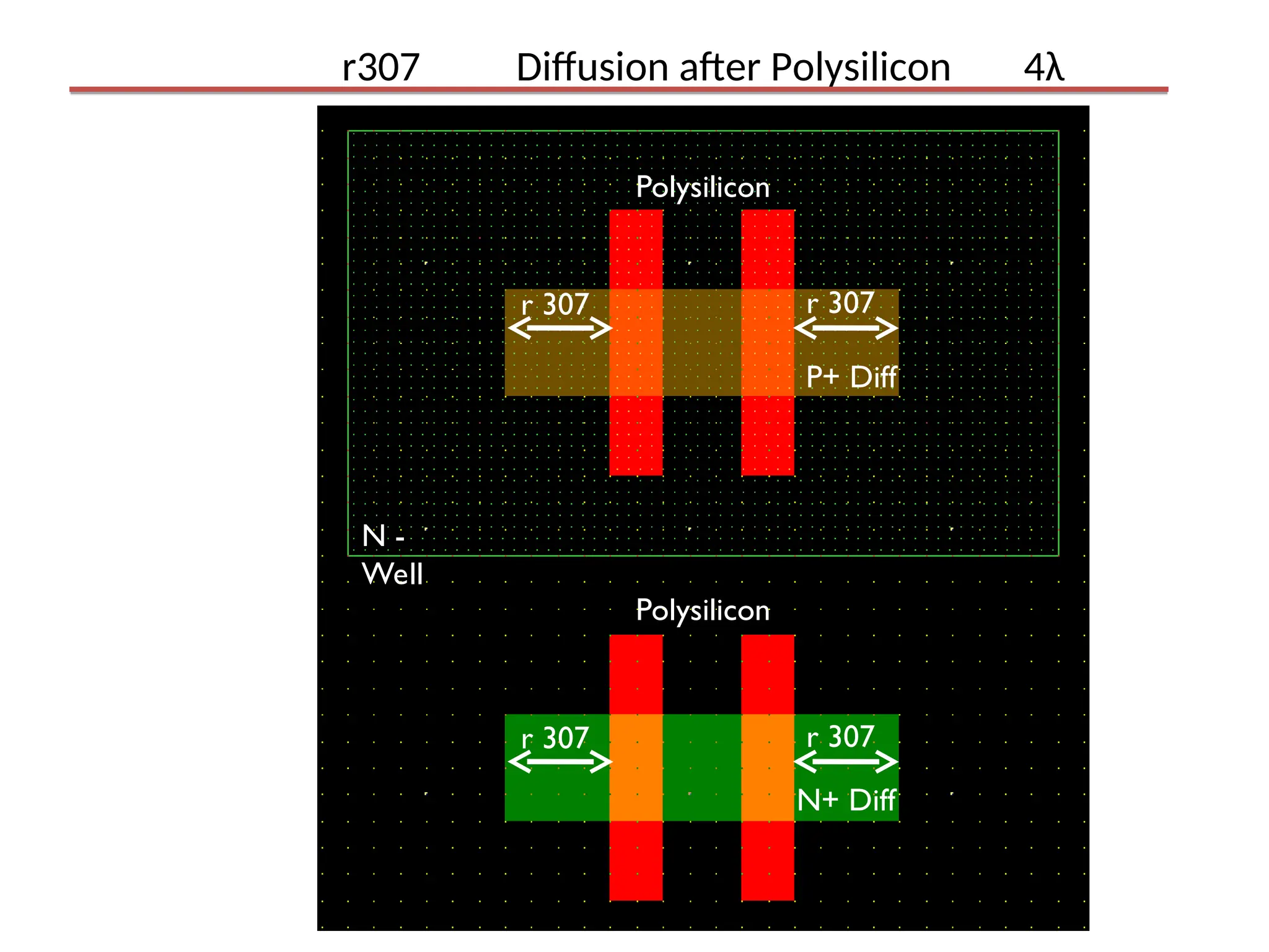
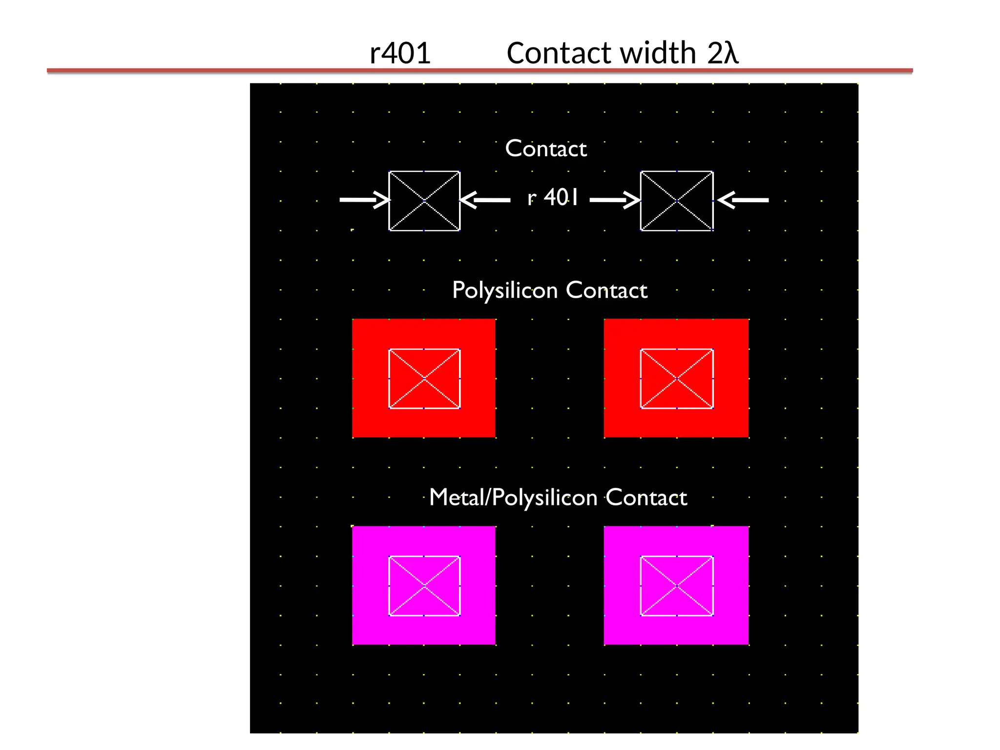
r203 Extra N-wellafter P+ diffusion 6λ
N -
Well
P+ Diff
N+ Diff
r 203
r 203
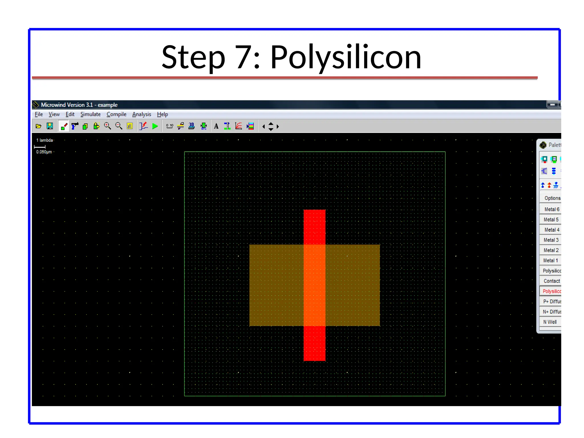
23.
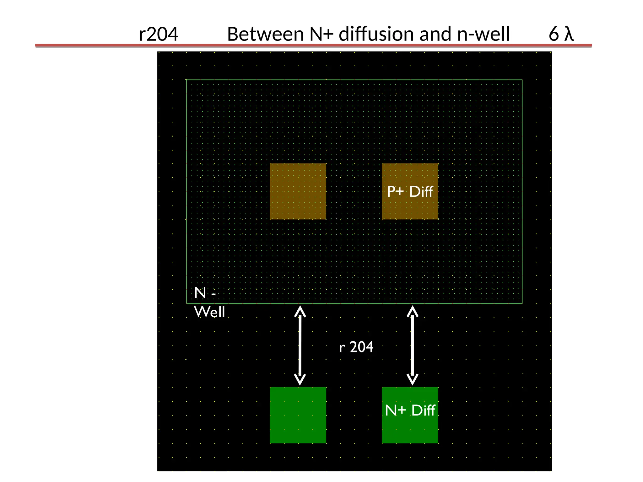
r204 Between N+diffusion and n-well 6 λ
r 204
N -
Well
P+ Diff
N+ Diff
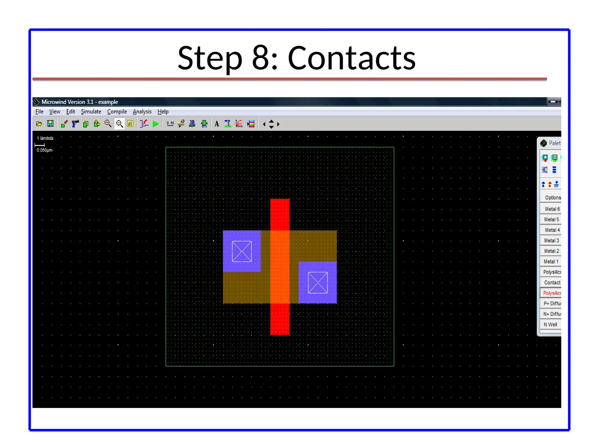
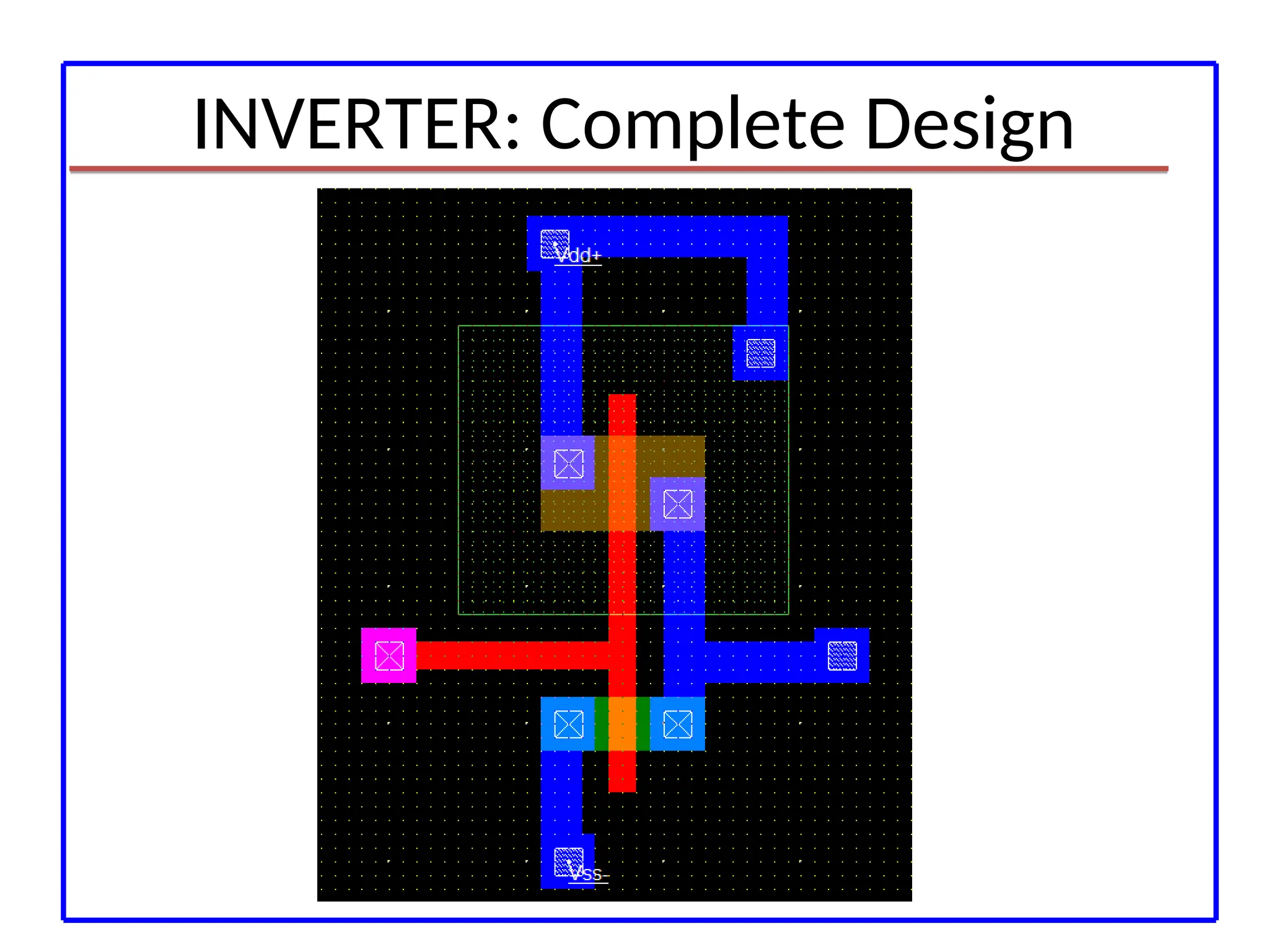
Final Connections
• pMOSCompleted
• Now Interconnection of pMOS and nMOS to
complete inverter
• Connect Source of pMOS to VDD and Source of
nMOS to VSS.
• Short the Drain of both pMOS and nMOS.
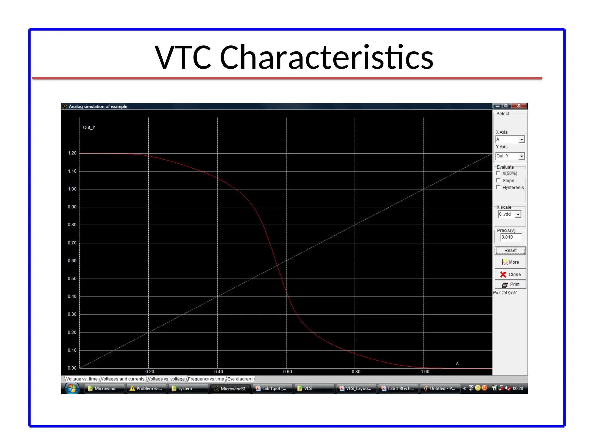
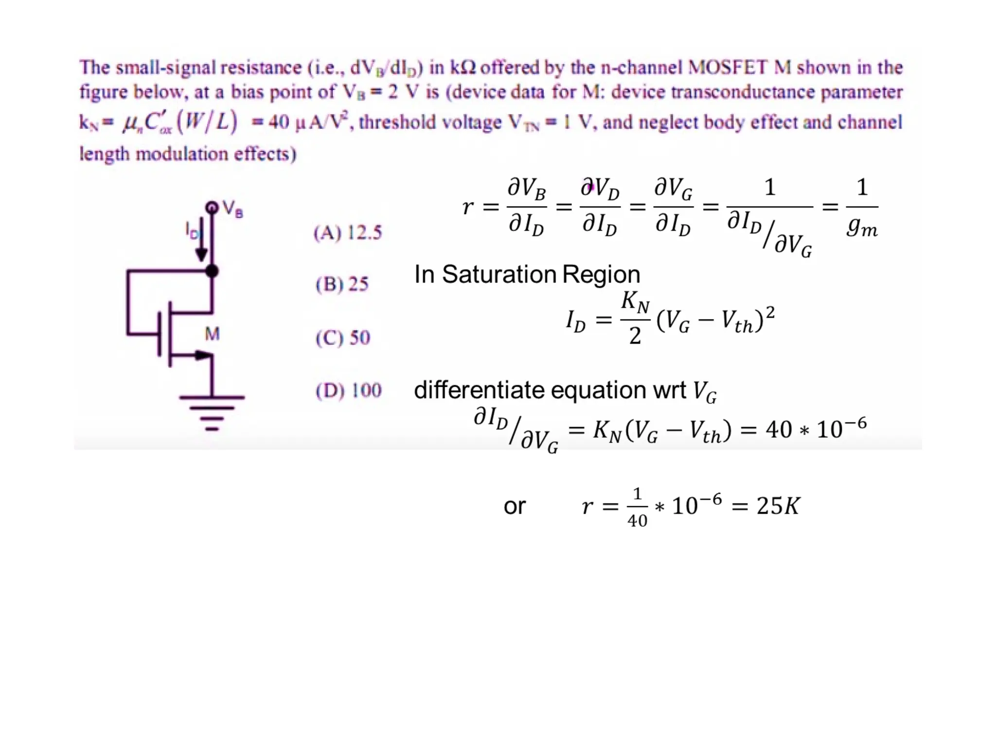
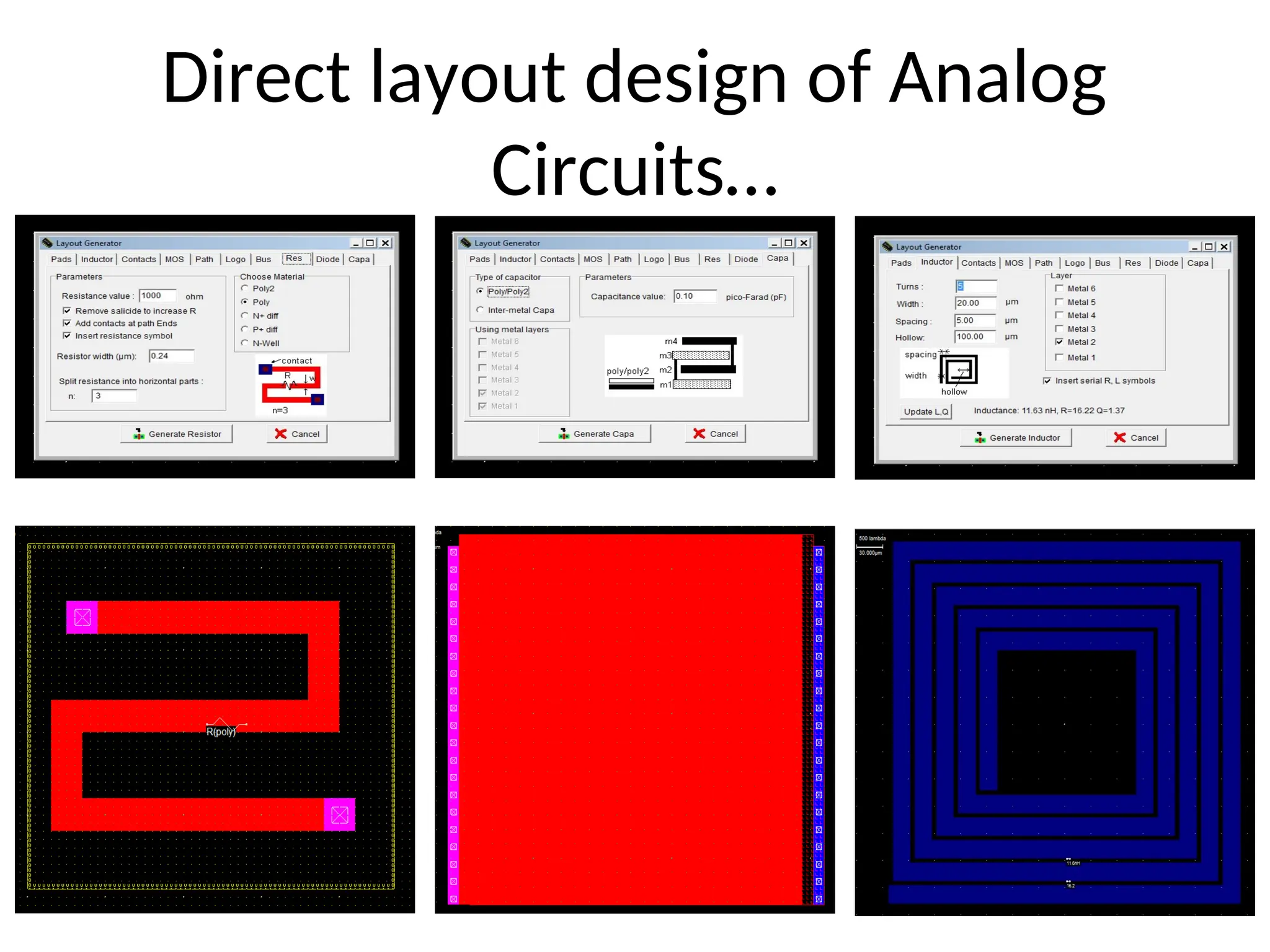
For Analog Circuits
(R,L and C Components)
if drain and gate is shorted then MOS will behave as a diode connected load
and it will never go to triode region and can be used as resistive load offering a
resistance equal to 1/gm.
if drain and source is shorted then MOS capacitor in which SiO2 will behave as
insulator.
#2 References
I am grateful for the contributions from SEMATECH, the Austin Community College, and MKS Instruments.
For further reading, I especially recommend the reference from Scientific American.
#3 References
I am grateful for the contributions from SEMATECH, the Austin Community College, and MKS Instruments.
For further reading, I especially recommend the reference from Scientific American.
#4 References
I am grateful for the contributions from SEMATECH, the Austin Community College, and MKS Instruments.
For further reading, I especially recommend the reference from Scientific American.
#5 References
I am grateful for the contributions from SEMATECH, the Austin Community College, and MKS Instruments.
For further reading, I especially recommend the reference from Scientific American.
#6 References
I am grateful for the contributions from SEMATECH, the Austin Community College, and MKS Instruments.
For further reading, I especially recommend the reference from Scientific American.
#7 References
I am grateful for the contributions from SEMATECH, the Austin Community College, and MKS Instruments.
For further reading, I especially recommend the reference from Scientific American.
#8 References
I am grateful for the contributions from SEMATECH, the Austin Community College, and MKS Instruments.
For further reading, I especially recommend the reference from Scientific American.
#9 References
I am grateful for the contributions from SEMATECH, the Austin Community College, and MKS Instruments.
For further reading, I especially recommend the reference from Scientific American.
#10 References
I am grateful for the contributions from SEMATECH, the Austin Community College, and MKS Instruments.
For further reading, I especially recommend the reference from Scientific American.
#11 References
I am grateful for the contributions from SEMATECH, the Austin Community College, and MKS Instruments.
For further reading, I especially recommend the reference from Scientific American.
#12 References
I am grateful for the contributions from SEMATECH, the Austin Community College, and MKS Instruments.
For further reading, I especially recommend the reference from Scientific American.
#13 References
I am grateful for the contributions from SEMATECH, the Austin Community College, and MKS Instruments.
For further reading, I especially recommend the reference from Scientific American.
#38 References
I am grateful for the contributions from SEMATECH, the Austin Community College, and MKS Instruments.
For further reading, I especially recommend the reference from Scientific American.
#39 References
I am grateful for the contributions from SEMATECH, the Austin Community College, and MKS Instruments.
For further reading, I especially recommend the reference from Scientific American.
#40 References
I am grateful for the contributions from SEMATECH, the Austin Community College, and MKS Instruments.
For further reading, I especially recommend the reference from Scientific American.
#41 References
I am grateful for the contributions from SEMATECH, the Austin Community College, and MKS Instruments.
For further reading, I especially recommend the reference from Scientific American.
#42 References
I am grateful for the contributions from SEMATECH, the Austin Community College, and MKS Instruments.
For further reading, I especially recommend the reference from Scientific American.
#43 References
I am grateful for the contributions from SEMATECH, the Austin Community College, and MKS Instruments.
For further reading, I especially recommend the reference from Scientific American.
#44 References
I am grateful for the contributions from SEMATECH, the Austin Community College, and MKS Instruments.
For further reading, I especially recommend the reference from Scientific American.
#45 References
I am grateful for the contributions from SEMATECH, the Austin Community College, and MKS Instruments.
For further reading, I especially recommend the reference from Scientific American.
#46 References
I am grateful for the contributions from SEMATECH, the Austin Community College, and MKS Instruments.
For further reading, I especially recommend the reference from Scientific American.
#47 References
I am grateful for the contributions from SEMATECH, the Austin Community College, and MKS Instruments.
For further reading, I especially recommend the reference from Scientific American.
#48 References
I am grateful for the contributions from SEMATECH, the Austin Community College, and MKS Instruments.
For further reading, I especially recommend the reference from Scientific American.
#49 References
I am grateful for the contributions from SEMATECH, the Austin Community College, and MKS Instruments.
For further reading, I especially recommend the reference from Scientific American.
#50 References
I am grateful for the contributions from SEMATECH, the Austin Community College, and MKS Instruments.
For further reading, I especially recommend the reference from Scientific American.
#51 References
I am grateful for the contributions from SEMATECH, the Austin Community College, and MKS Instruments.
For further reading, I especially recommend the reference from Scientific American.
#52 References
I am grateful for the contributions from SEMATECH, the Austin Community College, and MKS Instruments.
For further reading, I especially recommend the reference from Scientific American.
#53 When Drain and gate are short mosfet is in saturation.
#56 References
I am grateful for the contributions from SEMATECH, the Austin Community College, and MKS Instruments.
For further reading, I especially recommend the reference from Scientific American.