The document describes an experiment to generate and simulate a CMOS inverter circuit layout using the Microwind CAD tool. The key steps are:
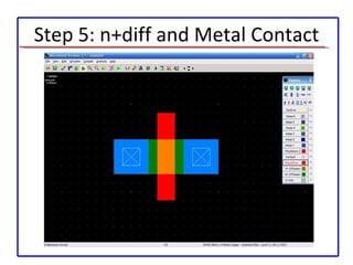
1. Select a foundry process and design the nMOS transistor by adding n-well, n+ diffusion, polysilicon, and metal contacts.
2. Design the pMOS transistor by adding an n-well, p+ diffusion, polysilicon, and contacts.
3. Interconnect the pMOS and nMOS transistors to form an inverter, connecting inputs, outputs, and power terminals.
4. Perform DRC checks and post-layout simulation to verify the inverter's transfer characteristics.