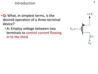
1
Introduction
•Q: What, in simplest terms, is the
desired operation of a three-terminal
device?
•A: Employ voltage between two
terminals to control current flowing
in to the third.
2
Introduction
• Q: What are two major types of
three-terminal semiconductor
devices?
• metal-oxide-semiconductor field-effect
transistor (MOSFET)
• bipolar junction transistor (BJT)
• Q: Why are MOSFET’s more widely
used?
• size (smaller)
• ease of manufacture
• consume less power
• MOSFET technology
• It allows placement of approximately 2
billion transistors on a single IC
• backbone of very large
scale integration (VLSI)
• It is considered preferable to BJT
technology for many applications.
3
Oxford University Publishing
Microelectronic Circuits by Adel S. Sedra and Kenneth C. Smith (0195323033)
5.1. Device Structure and Operation
• Figure 5.1. shows general structure of the n-channel enhancement-type
MOSFET
Figure 5.1: Physical structure of the enhancement-type NMOS transistor: (a) perspective view, (b) cross-
section. Note that typically L = 0.03um to 1um, W = 0.1um to 100um, and the thickness of the oxide
layer (tox) is in the range of 1 to 10nm.
4
Oxford University Publishing
Microelectronic Circuits by Adel S. Sedra and Kenneth C. Smith (0195323033)
5.1. Device Structure and Operation
Figure 5.1: Physical structure of the enhancement-type NMOS transistor: (a) perspective view, (b) cross-
section. Note that typically L = 0.03um to 1um, W = 0.1um to 100um, and the thickness of the oxide
layer (tox) is in the range of 1 to 10nm.
one p-type doped region
two n-type doped
regions (drain, source)
layer of SiO2 separates
source and drain
metal, placed on top of
SiO2, forms gate
electrode
5
Layout of NMOS Transistor
Ref: Lecture 9 – MOSFET, Microelectronic Devices and Circuits, Fall 2005, MIT OpenCourseWare
Top View
(Masks)
Side View
(Fabricated
Device)
6
5.1. Device Structure and Operation
• The name MOSFET is derived from its physical structure
• However, many MOSFET’s do not actually use any “metal”, polysilicon is used
instead
• Another name for MOSFET is insulated gate FET, or IGFET
• The device is composed of two pn-junctions, however they maintain reverse
biasing at all times.
• Drain will always be at positive voltage with respect to source.
7
5.1.2. Operation with Zero Gate Voltage
• With zero voltage applied to gate,
two back-to-back diodes exist in
series between drain and source.
• “They” prevent current conduction
from drain to source when a voltage
vDS is applied.
• yielding very high resistance (1012ohms)
Figure 5.1: Physical structure
8
5.1.3. Creating a Channel for Current Flow
• Q: What happens if (1) source and
drain are grounded and (2) positive
voltage is applied to gate?
• step #1: vGS is applied to the gate
terminal, causing a positive build-up
of positive charge along metal
electrode.
• step #2: This build-up causes free
holes to be repelled from region of
p-type substrate under gate.
Figure 5.2: The enhancement-type NMOS transistor
with a positive voltage applied to the gate. An n
channel is induced at the top of the substrate
beneath the gate
9
• step #3: This migration results in the
uncovering of negative bound
charges, originally neutralized by the
free holes
• step #4: The positive gate voltage
also attracts electrons from the n+
source and drain regions into the
channel.
5.1.3. Creating a Channel for Current Flow
Figure 5.2: The enhancement-type NMOS transistor
with a positive voltage applied to the gate. An n
channel is induced at the top of the substrate
beneath the gate
10
• step #5: Once a sufficient number of
“these” electrons accumulate, an n-
region is created…
• connecting the source and drain
regions
• step #6: This provides path for
current flow between D and S.
5.1.3. Creating a Channel for Current Flow
Figure 5.2: The enhancement-type NMOS transistor
with a positive voltage applied to the gate. An n
channel is induced at the top of the substrate
beneath the gate
this induced channel is
also known as an
inversion layer
11
5.1.3. Creating a Channel for Current Flow
• threshold voltage (Vt) – is the
minimum value of vGS required to
form a conducting channel
between drain and source
• typically between 0.3 and 0.6Vdc
• field-effect – when positive vGS is
applied, an electric field develops
between the gate electrode and
induced n-channel – the
conductivity of this channel is
affected by the strength of field
• SiO2 layer acts as dielectric
• effective / overdrive voltage – is the
difference between vGS applied and
Vt.
• oxide capacitance (Cox) – is the
capacitance of the parallel plate
capacitor per unit gate area (F/m2)
(eq5.1) OV GS t
v v V
 
 
2
2
is permittivity of SiO 3.45 11 /
is thickness of SiO layer
2
(eq5.3) in /
ox
ox
ox
ox
ox
F m
t
C
t
F m


 

E
Vtn is used for n-type
MOSFET, Vtp is used for
p-channel
12
5.1.3. Creating a Channel for Current Flow
• Q: What is main requirement for n-
channel to form?
• A: The voltage across the oxide layer
must exceed Vt.
• For example, when vDS = 0…
• the voltage at every point along
channel is zero
• the voltage across the oxide layer is
uniform and equal to vGS
• Q: How can one express the
magnitude of electron charge
contained in the channel?
• Q: What is effect of vOV on n-
channel?
• A: As vOV increases, so does the depth
of the n-channel as well as its
conductivity.
 
and represent width and length of channel respectively
(eq5.2) in
ox O
W L
V
Q C WL v C

13
5.1.4. Applying a small vDS
•Q: For small values of vDS, how does one calculate iDS
( iD)?
 
2
2
represents mobility of electrons at surface of the
n-channel in /
charge per unit
length of electron
-channel drift velocity
in / in /
(eq5 ) i
.7 n
n
m Vs
n
C m m Vs
n DS
D ox OV
v
i C W
L
A
v


 
  
 
14
•Q: What can be observed from equation (5.7)?
•A: For small values of vDS, the n-channel acts like a
variable resistance whose value is controlled by vOV (vOV
=vGS -vt)
5.1.4. Applying a small vDS
 
 
process
aspect
transconductance
ratio
parameter
(eq5.7) in
(eq5.8a)
1
in
D n ox OV DS
DS
DS
D
n ox OV
W
i C v v
L
v
r
W
i
C v
L
A


 
  
 
 
 





15
5.1.4. Applying a small vDS
•Q: What do we note from equation (5.7)?
•A: For small values of vDS, the n-channel acts like a
variable resistance whose value is controlled by vOV.
 
 
process
aspect
transconductance
ratio
parameter
(eq5.7) in
(eq5.8a)
1
in
D n ox OV DS
DS
DS
D
n ox OV
W
i C v v
L
v
r
W
i
C v
L
A


 
  
 
 
 





Note that this vOV represents
the depth of the n-channel -
what if it is not assumed to
be constant? How does this
equation change?
VERY IMPORTANT equation
16
5.1.4. Applying a Small vDS
•Q: What is rDS?
•A: rDS is the channel resistance
•Q: What three factors is rDS dependent on?
•A: process transconductance parameter for NMOS
(nCox) – which is determined by the manufacturing
process
•A: aspect ratio (W/L) – which is dependent on size
requirements / allocations
•A: overdrive voltage (vOV) – which is applied by the user
17
Oxford University Publishing
Microelectronic Circuits by Adel S. Sedra and Kenneth C. Smith (0195323033)
1/rDS
Figure 5.4: The iD-vDS characteristics of the MOSFET in Figure 5.3.
when the voltage applied between drain and source VDS is kept small.
high resistance, low vOV
low resistance, high vOV
kn is known as NMOS-FET
transconductance parameter
and is defined as nCoxW/L
18
5.1.5. Operation as vDS is Increased
•Q: What happens to iD when vDS increases beyond small
values?
•A: The relationship between them ceases to be linear.
•Q: How can this non-linearity be explained?
•step #1: Assume that vGS is held constant at value
greater than Vt.
•step #2: Also assume that vDS is applied and appears as
voltage drop across n-channel.
•step #3: Note that voltage decreases from vGS at the
source end of channel to vGD at drain end, where…
•vGD = vGS – vDS
•vGD = Vt + vOV – vDS
19
Oxford University Publishing
Microelectronic Circuits by Adel S. Sedra and Kenneth C. Smith (0195323033)
Figure 5.5: Operation of the enhancement NMOS transistor as vDS is
increased
avDS
avOV
The voltage differential
between both sides of n-
channel increases with vDS.
20
Figure 5.6(a): For a MOSFET with vGS = Vt + vOV , application of vDS causes the voltage drop along the
channel to vary linearly, with an average value of 0.5vDS at the midpoint. Since vGD > Vt, the channel still
exists at the drain end. (b) The channel shape corresponding to the situation in (a). While the depth of
the channel at the source is still proportional to vOV, the drain end is not.
note the average value
As vDS is increased,
the channel becomes
more tapered and
channel resistance
increases
EE 3110 Microelectronics I Suketu Naik
21
Oxford University Publishing
Microelectronic Circuits by Adel S. Sedra and Kenneth C. Smith (0195323033)
Q: How can this non-linearity be explained?
 step #4: Define
iDS in terms of vDS
and vOV.
   
   
   
1
2
if then
1
2
repl
1
2
1
ace
w
2
ith
(eq5.7)
if
ot
(eq5.7)
herwise
(eq5.14)
DS OV
OV O
D
V D
S O
S
V
DS OV
v v
D n ox OV DS DS
n ox OV DS DS
n ox OV DS
v v
D
v
v
DS
v
W
i C v v v
L
W
C v v v
v v
L
W
C v
i
v v
L



 


 
 
 
 
 
 
 




 




action:
   
 
1
2
2
1
if
in
otherwise
2
n ox OV DS DS
D
n O
DS OV
ox V
v
W
C v v v
L
i
C
L
v
A
W
v






 




triode vs. saturation region
iD is dependent on the
apparent vOV (not vDS
inherently) which does not
change after vDS > vOV
22
Oxford University Publishing
Microelectronic Circuits by Adel S. Sedra and Kenneth C. Smith (0195323033)
   
 
1
2
2
if
(eq5.14) in
othe
triode:
saturation:
1
s
2
rwi e
DS O
n ox OV DS DS
D
n O
V
ox V
W
C v v v
L
W
C v
L
v
i
v
A






 




saturation occurs
once vDS > vOV
23
5.1.6. Operation for vDS >> vOV
• In section 5.1.5, we assume that n-
channel is tapered but channel
pinch-off does not occur.
• Trapezoid doesn’t become triangle for
vGD > Vt
• Q: What happens if vDS > vOV?
• A: MOSFET enters saturation region.
• Any further increase in vDS has no
effect on iD.
Figure 5.8: Operation of MOSFET with vGS = Vt +
vOV as vDS is increased to vOV. At the drain end, vGD
decreases to Vt and the channel depth at the drain-
end reduces to zero (pinch-off). At this point, the
MOSFET enters saturation more of operation.
Further increasing vDS (beyond vOV) has no effect on
the channel shape and iD remains constant.
pinch-off does not mean
blockage of current
24
Summary
•The equation used to
define iD depends on
relationship btw vDS
and vOV.
•vDS << vOV
•vDS < vOV
•vDS => vOV
•vDS >> vOV
 
2
2
represents mobility of electrons at surface of the
n-channel in /
charge per unit
length of electron
-channel drift velocity
in / in /
(eq5.7) in
n
m Vs
n
C m m
n DS
D ox V
Vs
O
v
i C W A
v
L


 
  
 
   
 
   
1
2
2
2
1
2
(eq5.14) in
(eq5.17) in
(eq5.23) i
1
1 n
2
D n ox OV DS DS
D n ox OV
D n ox OV DS
W
i C v v v
L
W
i C v
L
W
i
A
v
L
A
C v
A


 
 

 
25
•Figure 5.11 shows an n-
channel enhancement
MOSFET.
•There are four terminals:
•drain (D), gate (G), body
(B), and source (S).
•Usually it is assumed that
body and source are
connected.
n-channel MOSFET (NMOS)
26
n-channel MOSFET (NMOS)
Gap indicates insulation (oxide) between
the gate electrode (G) and the Body (B)
This arrow from Body (p-type) to the n-
channel (n-type) indicates pn junction and
hence the type of device (n channel mosfet)
This arrow indicates the current going into the
source and thus indicates the type of device
(n channel mosfet)
27
NMOS Symbol
• Although MOSFET is symmetrical
device, one often designates
terminals as source and drain.
• Q: How does one make this
designation?
• A: By polarity of voltage applied.
• Arrowheads designate “normal”
direction of current flow
• Note that, in part (b), we designate
current as DS.
• No need to place arrow with B.
the potential at drain (vD) is
always positive with respect to
source (vS)
28
NMOS Symbol
• Although MOSFET is symmetrical
device, one often designates
terminals as source and drain.
• Q: How does one make this
designation?
• A: By polarity of voltage applied.
• Arrowheads designate “normal”
direction of current flow
• Note that, in part (b), we designate
current as DS.
• No need to place arrow with B.
the potential at drain (vD) is
always positive with respect to
source (vS)
29
Representations of NMOS Transistor
30
Regions of Operation of Enhancement NMOS
Tabe 5.1
31
iD -vDS characterstics of Enhancement NMOS
 Keep vGS constant
and vary vDS
32
iD -vGS characterstics of Enhancement NMOS
 Keep vDS constant (vDS >
vOV; saturation) and vary
vGS
 These charactertics are
useful for amplification
 
2
2
(eq5.21)
this relationship provides
basis for application of
MOSFET as amplifier
1
2
OV
D n GS tn
v
W
i k v V
L
 

 
 
 
33
 Vary vGS
 Voltage controlled
current Source
 Useful for
amplification
iD -vGS characterstics of Enhancement NMOS
 
2
2
(eq5.21)
this relationship provides
basis for application of
MOSFET as amplifier
1
2
OV
D n GS tn
v
W
i k v V
L
 

 
 
 
34
Large signal model of NMOS in saturation
MOSFET in saturation behaves as a voltage controlled
current source
35
Example 5.2: NMOS Transistor
Consider an NMOS transistor fabricated in an 0.18-m process with L = 0.18m
and W = 2m. The process technology is specified to have Cox = 8.6fF/m2, n =
450cm2/Vs, and Vtn = 0.5V.
•Q(a): Find VGS and VDS that result in the MOSFET operating at the edge of
saturation with ID = 100A
•Q(b): If VGS is kept constant, find VDS that results in ID = 50A
•Q(c): To investigate the use of the MOSFET as a linear amplifier, let it be
operating in saturation with VDS = 0.3V. Find the change in iD resulting from vGS
changing from 0.7V by +0.01V and -0.01V
36
5.2.4. Finite Output Resistance in Saturation
 
   
2
2
valid when
valid when
(eq5.17) in
(eq5.2
1
2
1
1
3) in
2
DS OV
DS OV
D n ox OV
D n ox OV D
v
S
v
v v
W
i C v
L
W
i C v v A
L
A

 



 
Figure 5.16: Increasing vDS beyond vDSsat causes
the channel pinch-off point to move slightly away
from the drain, thus reducing the effective channel
length by DL
Q: What effect will increased
vDS have on n-channel once
pinch-off has occurred?
A: Addition of finite output
resistance (ro).
Q: What is the effect on iD?
37
5.2.4. Output Resistance in Saturation
Q: How is ro defined?
• step #1: Note that ro is the 1/slope of iD-vDS
characteristic.
• step #2: Define relationship between iD
and vDS using (5.23).
• step #3: Take derivative of this function.
• step #4: Use above to define ro.
• Note that ro is defined in terms of iD,
where iD does not take in to account
channel length modulation
38
5.2.4. Finite Output Resistance in Saturation
Q: What is ?
• A: A device parameter with the units of V -1,
the value of which depends on
manufacturer’s design and manufacturing
process.
• Figure 5.17 demonstrates the effect of
channel length modulation on iD - vDS
curves
• In short, we can draw a straight line
between VA and saturation.
Figure 5.17: Effect of vDS on iD in the
saturation region. The MOSFET
parameter VA depends on the process
technology and, for a given process, is
proportional to the channel length L.
39
Exercise 5.6: Channel length modulation effect
NMOS transistor fabricated in an 0.4-m process with W = 16 m , L = 0.8 m,VA'
= 50 V/m, n Cox= 200 A/V2.
Q(a): Find VA and λ.
Q(b): Find ID if VOV = 0.5 V and VDS = 1 V.
Q(c): Find rO.
Q(b): Find the change in ID if VOV is increased by 2 V
40
5.1.7. The p-Channel MOSFET
• Figure 5.9(a): cross-sectional view of
a p-channel enhancement-type
MOSFET.
• structure is similar but current is
opposite to the n-channel
• Complementary devices – two
devices such as the p-channel and
n-channel MOSFETs.
41
5.1.7. The p-Channel MOSFET
• Q: What are main differences
between n-channel and p-channel?
• A: Negative voltage applied to gate
• allowing path for current
flow
• A: Threshold voltage is represented as
Vtp
• |vGS| > |Vtp|
42
5.1.7. The p-Channel MOSFET
• Q: What are main differences
between n-channel and p-channel?
• A: Process transconductance
parameters are defined differently
• k’p = pCox
• kp = pCox(W/L)
• A: The rest, essentially, is the same,
but with reverse polarity...
43
5.1.7. The p-Channel MOSFET
44
PMOS Equations: Table 5.2
 
 
   
  























2
,
2
,
2
,
2
,
2
1
1
2
1
2
1
)
1
(
2
1
SD
SD
tp
SG
ox
p
tri
D
SD
tp
SG
ox
p
sat
D
DS
DS
tp
GS
ox
p
tri
D
DS
tp
GS
ox
p
sat
D
V
V
V
V
L
W
C
I
V
V
V
L
W
C
I
V
V
V
V
L
W
C
I
V
V
V
L
W
C
I






ID
45
5.1.7. The p-Channel MOSFET (PMOS)
•Q: Why is NMOS advantageous over PMOS?
•A: Because electron mobility n is 2 – 4 times greater
than hole mobility p.
•Complementary MOS (CMOS) technology – is technology
which allows fabrication of both N and PMOS transistors
on a single chip.
46
5.2.5. Characteristics of the p-channel MOSFET
• Characteristics of the p-channel
MOSFET are similar to the n-channel,
however with signs reversed.
• Please review section 5.2.5 from the
text, with focus on table 5.2.
47
iD-vDS Characteristics of the p-channel MOSFET
Note:
1) In Fig.1(a) and (b) VSG > 0, VSD > 0 and iD > 0
2) In Fig.2 (a) and (b) VGS < 0, VDS < 0 and iD < 0 (opposite direction than in Fig. 1
Fig.1 (b)
Fig.2(b)
Fig.1 (a)
Fig.2(a)
-
vGS
+
-
vDS
+
+
vGD
-
48
PMOS Transistor
Exercise 5.7: PMOS Transistor
•Vtp = -1 V, kp'=pCox = 60A/V2
•W/L = 10
(a) Find the range of VG in which transistor
conducts
(b) In terms of VG, find the range of VD for
which transistor is in triode region
(c) In terms of VG, find the range of VD for
which transitor is in saturation region
(d) Neglect channel length modulation
effect and find values of |VOV| and VG
49
Oxford University Publishing
Microelectronic Circuits by Adel S. Sedra and Kenneth C. Smith (0195323033)
5.1.8. Complementary MOS or CMOS
•CMOS employs MOS transistors of both polarities
•more difficult to fabricate
•more powerful and flexible
•now more prevalent than NMOS or PMOS by itself
50
Oxford University Publishing
Microelectronic Circuits by Adel S. Sedra and Kenneth C. Smith (0195323033)
Figure 5.10: Cross-section of a CMOS integrated circuit. Note that the PMOS transistor is formed in a separate
n-type region, known as an n well. Another arrangement is also possible in which an n-type body is used and the
n device is formed in a p well. Not shown are the connections made to the p-type body and to the n well; the
latter functions as the body terminal for the p-channel device.
p-type semiconductor
provides the MOS body
(and allows generation of
n-channel)
n-well is added to allow
generation of p-channel
SiO2 is used to isolate
NMOS from PMOS

mos character..ppt

  • 1.
    1 Introduction •Q: What, insimplest terms, is the desired operation of a three-terminal device? •A: Employ voltage between two terminals to control current flowing in to the third.
  • 2.
    2 Introduction • Q: Whatare two major types of three-terminal semiconductor devices? • metal-oxide-semiconductor field-effect transistor (MOSFET) • bipolar junction transistor (BJT) • Q: Why are MOSFET’s more widely used? • size (smaller) • ease of manufacture • consume less power • MOSFET technology • It allows placement of approximately 2 billion transistors on a single IC • backbone of very large scale integration (VLSI) • It is considered preferable to BJT technology for many applications.
  • 3.
    3 Oxford University Publishing MicroelectronicCircuits by Adel S. Sedra and Kenneth C. Smith (0195323033) 5.1. Device Structure and Operation • Figure 5.1. shows general structure of the n-channel enhancement-type MOSFET Figure 5.1: Physical structure of the enhancement-type NMOS transistor: (a) perspective view, (b) cross- section. Note that typically L = 0.03um to 1um, W = 0.1um to 100um, and the thickness of the oxide layer (tox) is in the range of 1 to 10nm.
  • 4.
    4 Oxford University Publishing MicroelectronicCircuits by Adel S. Sedra and Kenneth C. Smith (0195323033) 5.1. Device Structure and Operation Figure 5.1: Physical structure of the enhancement-type NMOS transistor: (a) perspective view, (b) cross- section. Note that typically L = 0.03um to 1um, W = 0.1um to 100um, and the thickness of the oxide layer (tox) is in the range of 1 to 10nm. one p-type doped region two n-type doped regions (drain, source) layer of SiO2 separates source and drain metal, placed on top of SiO2, forms gate electrode
  • 5.
    5 Layout of NMOSTransistor Ref: Lecture 9 – MOSFET, Microelectronic Devices and Circuits, Fall 2005, MIT OpenCourseWare Top View (Masks) Side View (Fabricated Device)
  • 6.
    6 5.1. Device Structureand Operation • The name MOSFET is derived from its physical structure • However, many MOSFET’s do not actually use any “metal”, polysilicon is used instead • Another name for MOSFET is insulated gate FET, or IGFET • The device is composed of two pn-junctions, however they maintain reverse biasing at all times. • Drain will always be at positive voltage with respect to source.
  • 7.
    7 5.1.2. Operation withZero Gate Voltage • With zero voltage applied to gate, two back-to-back diodes exist in series between drain and source. • “They” prevent current conduction from drain to source when a voltage vDS is applied. • yielding very high resistance (1012ohms) Figure 5.1: Physical structure
  • 8.
    8 5.1.3. Creating aChannel for Current Flow • Q: What happens if (1) source and drain are grounded and (2) positive voltage is applied to gate? • step #1: vGS is applied to the gate terminal, causing a positive build-up of positive charge along metal electrode. • step #2: This build-up causes free holes to be repelled from region of p-type substrate under gate. Figure 5.2: The enhancement-type NMOS transistor with a positive voltage applied to the gate. An n channel is induced at the top of the substrate beneath the gate
  • 9.
    9 • step #3:This migration results in the uncovering of negative bound charges, originally neutralized by the free holes • step #4: The positive gate voltage also attracts electrons from the n+ source and drain regions into the channel. 5.1.3. Creating a Channel for Current Flow Figure 5.2: The enhancement-type NMOS transistor with a positive voltage applied to the gate. An n channel is induced at the top of the substrate beneath the gate
  • 10.
    10 • step #5:Once a sufficient number of “these” electrons accumulate, an n- region is created… • connecting the source and drain regions • step #6: This provides path for current flow between D and S. 5.1.3. Creating a Channel for Current Flow Figure 5.2: The enhancement-type NMOS transistor with a positive voltage applied to the gate. An n channel is induced at the top of the substrate beneath the gate this induced channel is also known as an inversion layer
  • 11.
    11 5.1.3. Creating aChannel for Current Flow • threshold voltage (Vt) – is the minimum value of vGS required to form a conducting channel between drain and source • typically between 0.3 and 0.6Vdc • field-effect – when positive vGS is applied, an electric field develops between the gate electrode and induced n-channel – the conductivity of this channel is affected by the strength of field • SiO2 layer acts as dielectric • effective / overdrive voltage – is the difference between vGS applied and Vt. • oxide capacitance (Cox) – is the capacitance of the parallel plate capacitor per unit gate area (F/m2) (eq5.1) OV GS t v v V     2 2 is permittivity of SiO 3.45 11 / is thickness of SiO layer 2 (eq5.3) in / ox ox ox ox ox F m t C t F m      E Vtn is used for n-type MOSFET, Vtp is used for p-channel
  • 12.
    12 5.1.3. Creating aChannel for Current Flow • Q: What is main requirement for n- channel to form? • A: The voltage across the oxide layer must exceed Vt. • For example, when vDS = 0… • the voltage at every point along channel is zero • the voltage across the oxide layer is uniform and equal to vGS • Q: How can one express the magnitude of electron charge contained in the channel? • Q: What is effect of vOV on n- channel? • A: As vOV increases, so does the depth of the n-channel as well as its conductivity.   and represent width and length of channel respectively (eq5.2) in ox O W L V Q C WL v C 
  • 13.
    13 5.1.4. Applying asmall vDS •Q: For small values of vDS, how does one calculate iDS ( iD)?   2 2 represents mobility of electrons at surface of the n-channel in / charge per unit length of electron -channel drift velocity in / in / (eq5 ) i .7 n n m Vs n C m m Vs n DS D ox OV v i C W L A v         
  • 14.
    14 •Q: What canbe observed from equation (5.7)? •A: For small values of vDS, the n-channel acts like a variable resistance whose value is controlled by vOV (vOV =vGS -vt) 5.1.4. Applying a small vDS     process aspect transconductance ratio parameter (eq5.7) in (eq5.8a) 1 in D n ox OV DS DS DS D n ox OV W i C v v L v r W i C v L A                  
  • 15.
    15 5.1.4. Applying asmall vDS •Q: What do we note from equation (5.7)? •A: For small values of vDS, the n-channel acts like a variable resistance whose value is controlled by vOV.     process aspect transconductance ratio parameter (eq5.7) in (eq5.8a) 1 in D n ox OV DS DS DS D n ox OV W i C v v L v r W i C v L A                   Note that this vOV represents the depth of the n-channel - what if it is not assumed to be constant? How does this equation change? VERY IMPORTANT equation
  • 16.
    16 5.1.4. Applying aSmall vDS •Q: What is rDS? •A: rDS is the channel resistance •Q: What three factors is rDS dependent on? •A: process transconductance parameter for NMOS (nCox) – which is determined by the manufacturing process •A: aspect ratio (W/L) – which is dependent on size requirements / allocations •A: overdrive voltage (vOV) – which is applied by the user
  • 17.
    17 Oxford University Publishing MicroelectronicCircuits by Adel S. Sedra and Kenneth C. Smith (0195323033) 1/rDS Figure 5.4: The iD-vDS characteristics of the MOSFET in Figure 5.3. when the voltage applied between drain and source VDS is kept small. high resistance, low vOV low resistance, high vOV kn is known as NMOS-FET transconductance parameter and is defined as nCoxW/L
  • 18.
    18 5.1.5. Operation asvDS is Increased •Q: What happens to iD when vDS increases beyond small values? •A: The relationship between them ceases to be linear. •Q: How can this non-linearity be explained? •step #1: Assume that vGS is held constant at value greater than Vt. •step #2: Also assume that vDS is applied and appears as voltage drop across n-channel. •step #3: Note that voltage decreases from vGS at the source end of channel to vGD at drain end, where… •vGD = vGS – vDS •vGD = Vt + vOV – vDS
  • 19.
    19 Oxford University Publishing MicroelectronicCircuits by Adel S. Sedra and Kenneth C. Smith (0195323033) Figure 5.5: Operation of the enhancement NMOS transistor as vDS is increased avDS avOV The voltage differential between both sides of n- channel increases with vDS.
  • 20.
    20 Figure 5.6(a): Fora MOSFET with vGS = Vt + vOV , application of vDS causes the voltage drop along the channel to vary linearly, with an average value of 0.5vDS at the midpoint. Since vGD > Vt, the channel still exists at the drain end. (b) The channel shape corresponding to the situation in (a). While the depth of the channel at the source is still proportional to vOV, the drain end is not. note the average value As vDS is increased, the channel becomes more tapered and channel resistance increases
  • 21.
    EE 3110 MicroelectronicsI Suketu Naik 21 Oxford University Publishing Microelectronic Circuits by Adel S. Sedra and Kenneth C. Smith (0195323033) Q: How can this non-linearity be explained?  step #4: Define iDS in terms of vDS and vOV.             1 2 if then 1 2 repl 1 2 1 ace w 2 ith (eq5.7) if ot (eq5.7) herwise (eq5.14) DS OV OV O D V D S O S V DS OV v v D n ox OV DS DS n ox OV DS DS n ox OV DS v v D v v DS v W i C v v v L W C v v v v v L W C v i v v L                                action:       1 2 2 1 if in otherwise 2 n ox OV DS DS D n O DS OV ox V v W C v v v L i C L v A W v             triode vs. saturation region iD is dependent on the apparent vOV (not vDS inherently) which does not change after vDS > vOV
  • 22.
    22 Oxford University Publishing MicroelectronicCircuits by Adel S. Sedra and Kenneth C. Smith (0195323033)       1 2 2 if (eq5.14) in othe triode: saturation: 1 s 2 rwi e DS O n ox OV DS DS D n O V ox V W C v v v L W C v L v i v A             saturation occurs once vDS > vOV
  • 23.
    23 5.1.6. Operation forvDS >> vOV • In section 5.1.5, we assume that n- channel is tapered but channel pinch-off does not occur. • Trapezoid doesn’t become triangle for vGD > Vt • Q: What happens if vDS > vOV? • A: MOSFET enters saturation region. • Any further increase in vDS has no effect on iD. Figure 5.8: Operation of MOSFET with vGS = Vt + vOV as vDS is increased to vOV. At the drain end, vGD decreases to Vt and the channel depth at the drain- end reduces to zero (pinch-off). At this point, the MOSFET enters saturation more of operation. Further increasing vDS (beyond vOV) has no effect on the channel shape and iD remains constant. pinch-off does not mean blockage of current
  • 24.
    24 Summary •The equation usedto define iD depends on relationship btw vDS and vOV. •vDS << vOV •vDS < vOV •vDS => vOV •vDS >> vOV   2 2 represents mobility of electrons at surface of the n-channel in / charge per unit length of electron -channel drift velocity in / in / (eq5.7) in n m Vs n C m m n DS D ox V Vs O v i C W A v L                    1 2 2 2 1 2 (eq5.14) in (eq5.17) in (eq5.23) i 1 1 n 2 D n ox OV DS DS D n ox OV D n ox OV DS W i C v v v L W i C v L W i A v L A C v A         
  • 25.
    25 •Figure 5.11 showsan n- channel enhancement MOSFET. •There are four terminals: •drain (D), gate (G), body (B), and source (S). •Usually it is assumed that body and source are connected. n-channel MOSFET (NMOS)
  • 26.
    26 n-channel MOSFET (NMOS) Gapindicates insulation (oxide) between the gate electrode (G) and the Body (B) This arrow from Body (p-type) to the n- channel (n-type) indicates pn junction and hence the type of device (n channel mosfet) This arrow indicates the current going into the source and thus indicates the type of device (n channel mosfet)
  • 27.
    27 NMOS Symbol • AlthoughMOSFET is symmetrical device, one often designates terminals as source and drain. • Q: How does one make this designation? • A: By polarity of voltage applied. • Arrowheads designate “normal” direction of current flow • Note that, in part (b), we designate current as DS. • No need to place arrow with B. the potential at drain (vD) is always positive with respect to source (vS)
  • 28.
    28 NMOS Symbol • AlthoughMOSFET is symmetrical device, one often designates terminals as source and drain. • Q: How does one make this designation? • A: By polarity of voltage applied. • Arrowheads designate “normal” direction of current flow • Note that, in part (b), we designate current as DS. • No need to place arrow with B. the potential at drain (vD) is always positive with respect to source (vS)
  • 29.
  • 30.
    30 Regions of Operationof Enhancement NMOS Tabe 5.1
  • 31.
    31 iD -vDS charactersticsof Enhancement NMOS  Keep vGS constant and vary vDS
  • 32.
    32 iD -vGS charactersticsof Enhancement NMOS  Keep vDS constant (vDS > vOV; saturation) and vary vGS  These charactertics are useful for amplification   2 2 (eq5.21) this relationship provides basis for application of MOSFET as amplifier 1 2 OV D n GS tn v W i k v V L         
  • 33.
    33  Vary vGS Voltage controlled current Source  Useful for amplification iD -vGS characterstics of Enhancement NMOS   2 2 (eq5.21) this relationship provides basis for application of MOSFET as amplifier 1 2 OV D n GS tn v W i k v V L         
  • 34.
    34 Large signal modelof NMOS in saturation MOSFET in saturation behaves as a voltage controlled current source
  • 35.
    35 Example 5.2: NMOSTransistor Consider an NMOS transistor fabricated in an 0.18-m process with L = 0.18m and W = 2m. The process technology is specified to have Cox = 8.6fF/m2, n = 450cm2/Vs, and Vtn = 0.5V. •Q(a): Find VGS and VDS that result in the MOSFET operating at the edge of saturation with ID = 100A •Q(b): If VGS is kept constant, find VDS that results in ID = 50A •Q(c): To investigate the use of the MOSFET as a linear amplifier, let it be operating in saturation with VDS = 0.3V. Find the change in iD resulting from vGS changing from 0.7V by +0.01V and -0.01V
  • 36.
    36 5.2.4. Finite OutputResistance in Saturation       2 2 valid when valid when (eq5.17) in (eq5.2 1 2 1 1 3) in 2 DS OV DS OV D n ox OV D n ox OV D v S v v v W i C v L W i C v v A L A         Figure 5.16: Increasing vDS beyond vDSsat causes the channel pinch-off point to move slightly away from the drain, thus reducing the effective channel length by DL Q: What effect will increased vDS have on n-channel once pinch-off has occurred? A: Addition of finite output resistance (ro). Q: What is the effect on iD?
  • 37.
    37 5.2.4. Output Resistancein Saturation Q: How is ro defined? • step #1: Note that ro is the 1/slope of iD-vDS characteristic. • step #2: Define relationship between iD and vDS using (5.23). • step #3: Take derivative of this function. • step #4: Use above to define ro. • Note that ro is defined in terms of iD, where iD does not take in to account channel length modulation
  • 38.
    38 5.2.4. Finite OutputResistance in Saturation Q: What is ? • A: A device parameter with the units of V -1, the value of which depends on manufacturer’s design and manufacturing process. • Figure 5.17 demonstrates the effect of channel length modulation on iD - vDS curves • In short, we can draw a straight line between VA and saturation. Figure 5.17: Effect of vDS on iD in the saturation region. The MOSFET parameter VA depends on the process technology and, for a given process, is proportional to the channel length L.
  • 39.
    39 Exercise 5.6: Channellength modulation effect NMOS transistor fabricated in an 0.4-m process with W = 16 m , L = 0.8 m,VA' = 50 V/m, n Cox= 200 A/V2. Q(a): Find VA and λ. Q(b): Find ID if VOV = 0.5 V and VDS = 1 V. Q(c): Find rO. Q(b): Find the change in ID if VOV is increased by 2 V
  • 40.
    40 5.1.7. The p-ChannelMOSFET • Figure 5.9(a): cross-sectional view of a p-channel enhancement-type MOSFET. • structure is similar but current is opposite to the n-channel • Complementary devices – two devices such as the p-channel and n-channel MOSFETs.
  • 41.
    41 5.1.7. The p-ChannelMOSFET • Q: What are main differences between n-channel and p-channel? • A: Negative voltage applied to gate • allowing path for current flow • A: Threshold voltage is represented as Vtp • |vGS| > |Vtp|
  • 42.
    42 5.1.7. The p-ChannelMOSFET • Q: What are main differences between n-channel and p-channel? • A: Process transconductance parameters are defined differently • k’p = pCox • kp = pCox(W/L) • A: The rest, essentially, is the same, but with reverse polarity...
  • 43.
  • 44.
    44 PMOS Equations: Table5.2                                   2 , 2 , 2 , 2 , 2 1 1 2 1 2 1 ) 1 ( 2 1 SD SD tp SG ox p tri D SD tp SG ox p sat D DS DS tp GS ox p tri D DS tp GS ox p sat D V V V V L W C I V V V L W C I V V V V L W C I V V V L W C I       ID
  • 45.
    45 5.1.7. The p-ChannelMOSFET (PMOS) •Q: Why is NMOS advantageous over PMOS? •A: Because electron mobility n is 2 – 4 times greater than hole mobility p. •Complementary MOS (CMOS) technology – is technology which allows fabrication of both N and PMOS transistors on a single chip.
  • 46.
    46 5.2.5. Characteristics ofthe p-channel MOSFET • Characteristics of the p-channel MOSFET are similar to the n-channel, however with signs reversed. • Please review section 5.2.5 from the text, with focus on table 5.2.
  • 47.
    47 iD-vDS Characteristics ofthe p-channel MOSFET Note: 1) In Fig.1(a) and (b) VSG > 0, VSD > 0 and iD > 0 2) In Fig.2 (a) and (b) VGS < 0, VDS < 0 and iD < 0 (opposite direction than in Fig. 1 Fig.1 (b) Fig.2(b) Fig.1 (a) Fig.2(a) - vGS + - vDS + + vGD -
  • 48.
    48 PMOS Transistor Exercise 5.7:PMOS Transistor •Vtp = -1 V, kp'=pCox = 60A/V2 •W/L = 10 (a) Find the range of VG in which transistor conducts (b) In terms of VG, find the range of VD for which transistor is in triode region (c) In terms of VG, find the range of VD for which transitor is in saturation region (d) Neglect channel length modulation effect and find values of |VOV| and VG
  • 49.
    49 Oxford University Publishing MicroelectronicCircuits by Adel S. Sedra and Kenneth C. Smith (0195323033) 5.1.8. Complementary MOS or CMOS •CMOS employs MOS transistors of both polarities •more difficult to fabricate •more powerful and flexible •now more prevalent than NMOS or PMOS by itself
  • 50.
    50 Oxford University Publishing MicroelectronicCircuits by Adel S. Sedra and Kenneth C. Smith (0195323033) Figure 5.10: Cross-section of a CMOS integrated circuit. Note that the PMOS transistor is formed in a separate n-type region, known as an n well. Another arrangement is also possible in which an n-type body is used and the n device is formed in a p well. Not shown are the connections made to the p-type body and to the n well; the latter functions as the body terminal for the p-channel device. p-type semiconductor provides the MOS body (and allows generation of n-channel) n-well is added to allow generation of p-channel SiO2 is used to isolate NMOS from PMOS