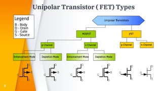
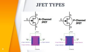
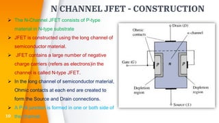
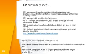
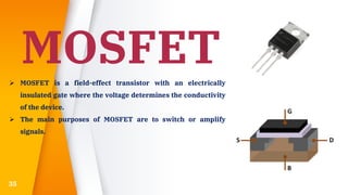
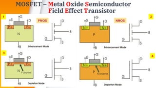
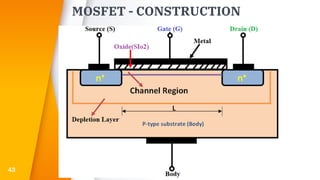
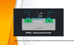
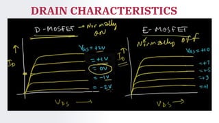
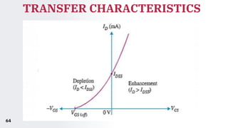
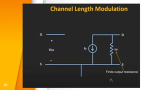
FIELD EFFECT
TRANSISTOR
Dr.S.Muthumanickam, BE., ME., Ph.D.,
Associate Professor
Department of Electronics and Communication Engineering
RMK College of Engineering and Technology
TOPICS
▸ JFETs
▸ Drain and Transfer characteristics,
▸ Current equations
▸ Pinch off voltage and its
significance
▸ MOSFET
▸ Characteristics
▸ Threshold voltage
▸ Channel length modulation
▸ D-MOSFET
▸ E-MOSFET
▸ Characteristics
▸ Comparison of MOSFET with JFET
2
FIELD EFFECT TRANSISTOR (FET)
3
 Field-effect transistor (FET) - electric field to
control the flow of current.
 Three terminals: source, gate, and drain.
 FETs control the flow of current by the application of
a voltage to the gate(voltage controlled device)
 FETs are unipolar transistors, use
either electrons or holes as charge carriers in their
operation, but not both.
 High input impedance.
 Less noise due to the absence of
minority carrier in Id.
TYPES OF FET
4
Unipolar Transistor ( FET) Types
5
6
JUNCTION FIELD EFFECT
TRANSISTOR (JFET)
7
TERMINALS
G – Gate
D – Drain
S - Source
JFET TYPES
8
Advantages of JFET
▸ A JFET is a voltage controlled, constant current device in which variation
in input voltage control the output current. Some of the advantages of
JFET are:
▸ It has a very high input impedance. This permits high degree of isolation
between the input and output circuits.
▸ The operation of a JFET depends upon the bulk material current carriers
that do not cross junctions. Therefore, the inherent noise of tubes and
those of transistors are not present in a JFET.
▸ A JFET has a negative temperature co-efficient of resistance. This avoids
the risk of thermal runaway.
▸ A JFET has a very high power gain. This eliminates the necessity of using
driver stages.
▸ A JFET has a smaller size, longer life and high efficiency
9
N CHANNEL JFET - CONSTRUCTION
10
 The N-Channel JFET consists of P-type
material in N-type substrate
 JFET is constructed using the long channel of
semiconductor material.
 JFET contains a large number of negative
charge carriers (refers as electrons)in the
channel is called N-type JFET.
 In the long channel of semiconductor material,
Ohmic contacts at each end are created to
form the Source and Drain connections.
 A P-N junction is formed in one or both side of
the channel.
N CHANNEL JFET - WORKING
11 FET operates with reverse bias PN junction to control current in a channel
12
13
14
PINCH – OFF VOLTAGE
15
For Vgs = 0v, the value of Vds at which Id
becomes constant is called pinch-off
voltage
B C
A
16
JFET CIRCUIT DIAGRAM
17
18
DRAIN CHARACTERISTICS
19
20
21
P CHANNEL JFET WORKING
22
Difference Between JFET and BJT
▸ In a JFET, there is only one type of carrier, i.e. holes in p-type channel and
electrons in n-type channel. For this reason it is also called unipolar
transistor. However, in an ordinary BJT, both electrons and holes play role
in conduction. Therefore, it is called as bipolar transistor.
▸ As the input circuit of a JFET is reverse biased, therefore, it has a high input
impedance. However, the input circuit of a BJT is forward biased and hence
has low input impedance.
▸ The primary functional difference between the JFET and BJT is that no
current enters the gate of JFET. However, in typical BJT base current might
be a few µA.
▸ A BJT uses the current into its base to control a large current between
collector and emitter. Whereas a JFET uses voltage on the gate terminal to
control the current between drain and source.
▸ In JFET, there is no junction. Therefore, noise level in JFET is very small.
23
24
25
https://www.allaboutcircuits.com/worksheets/junction-field-effect-transistors-
jfet/
https://www.gatepaper.in/2014/10/gate-practice-problems-on-jfet-
junction.html
https://www.allaboutcircuits.com/worksheets
26
27
28
29
30
31
32
33
34
MOSFET
35
 MOSFET is a field-effect transistor with an electrically
insulated gate where the voltage determines the conductivity
of the device.
 The main purposes of MOSFET are to switch or amplify
signals.
MOSFET
ENHANCEMENT MODE
MOSFET
N-Channel
MOSFET
P-channel
MOSFET
DEPLETION MODE
MOSFET
N-Channel
MOSFET
P-channel
MOSFET
37
MOSFET – Metal Oxide Semiconductor
Field Effect Transistor
38
NMOS
PMOS
1
4
3
2
39
40
41
42
MOSFET - CONSTRUCTION
43
Applications of MOSFET
▸ MOSFET is used in modern days calculators.
▸ It is used in microprocessors.
▸ It is used in integrated circuits.
▸ It is used in electronic chip cards or electronic
memories.
▸ It is used in logic CMOS gates.
▸ MOSFET is used in analog switches.
▸ It works as an amplifier.
▸ MOSFETs work as an oscillator.
▸ It is used in automobile sound systems.
44
MOSFET
CONSTRUCTION
45
ENHANCEMENT
MOSFET
E-MOSFET
52
MOSFET – Metal Oxide Semiconductor
Field Effect Transistor
53
54
55
56
https://www.circuitbread.com/tutorials/how-a-mosfet-works-at-the-semiconductor-level
DRAIN CHARACTERISTICS OF E-MOSFET
57
DEPLETION
MOSFET
D-MOSFET
58
DEPLETION MODE
MOSFET
DRAIN CHARACTERISTICS
TRANSFER CHARACTERISTICS
64
65
E-MOSFET
CHANNEL LENGTH
MODULATION
Length of the channel is varied
according to Vds
67
68
69
70
71
72
73
74
75
76
77
78
79
80
81
Finite output resistance
82

Field effect transistors