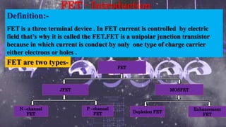
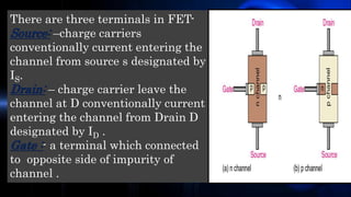
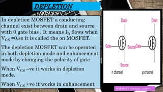
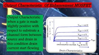
1
HARSHITA GUPTA
B.Sc 3rd year
1 1
History
Introduction of JFET
Construction and working JFET
Drain and transfer characteristics of JFET
MOSFET
Construction and working MOSFET
Drain and transfer characteristics of MOSFET
 Applications
Outlines
YEAR SCIENCETIST NAME INVENTION
1926
Julius Edger
Lilienfeld
First FET patents
(something same as
FET)
1934 Oskar Heil
Not actual FET but
concepts are FET like
devices .
1947
William Shockey
and his team
Failed attempt to
made FET (discovery
of first transistor or
PCT )
1959 Dawon Kahng MOSFET
HISTORY
FET - Introduction
Definition:-
FET is a three terminal device . In FET current is controlled by electric
field that’s why it is called the FET.FET is a unipolar junction transistor
because in which current is conduct by only one type of charge carrier
either electrons or holes .
FET
JFET MOSFET
N –channel
FET
P –channel
FET Depletion FET
Enhancement
FET
FET are two types-
In JFET a channel is form between the two heavily doped
with impurities opposite to that of bar . If the channel is n
type impurity then FET is called n channel FET. And if the
channel is p type impurity then it is called p channel FET.
ArepresentationofthebasicstructureofthetwotypesofJFET. J FET schema t ic sy mbo ls.
There are three terminals in FET-
Source: –charge carriers
conventionally current entering the
channel from source s designated by
IS.
Drain: – charge carrier leave the
channel at D conventionally current
entering the channel from Drain D
designated by ID .
Gate :- a terminal which connected
to opposite side of impurity of
channel .
I. Working of FET (Zero voltage
at the Gate)
VDS=VDD
VDD=2v
2v=4r
r=0.5v
Result
Width of depletion layer is more
at the top as compare to bottom
When VGS=0v
And VDS > 0 a current ID will
start flowing as soon as VDS
increase the width of depletion
layer increases at the top but
remains same at the bottom. Z
Z
Z
Z
Z
Z
Z
Z
Z
Z
Z
Z
r
S
D
r
r
r
2v
0v
1.5v
1v
0.5v
+
-
D
S
G
ID
p pn
e-
e-
VGS=0v
1.5v
0.5v
+
-
D
S
G
ID
p pn
e-
e-
VGS=0v
1.5v
0.5v
+
-
VDD
D
S
G
ID
p pn
e-
e-
VGS=0v
1.5v
0.5v
Working of FET(negative voltage at the gate )
When VGS = -ve
If VGS= -1 volte and we increase VDS the width
of depletion layer increasing greater than on
top as compare to bottom after some time we
can see to depletion layer to each other. This
condition is known as pinch of condition and
corresponding VDS is called the pinch of
voltage. If we increase VDS beyond pinch of
voltage ID remains constant which is called
saturation condition and this maximum
current is known as IDSS . Further increasing
VDS we get current increases rapidly at
particular voltage VDS . This voltage is known
as break down voltage.
+
-
D
S
G
ID
p pn
e-
e-
VGS=0v
1.5v
0.5v
+
-
D
S
G
ID
p pn
e-
e-
VGS=0v
1.5v
0.5v
+
-
D
S
G
ID
p pn
e-
e-
VGS=0v
1.5v
0.5v
+
-
D
S
ID
+
-
p p
The curve plotted
between ID and VDS
For different value of
VGS is called Output
or drain
characteristics of
JFET
 When VGS=0 and
VDS>|VP| then
IDSS=8ma
Ohmic
Region
A B
The maximum drain current is given by this
relation
This is a non linear equation if we decrease VGS
then ID will increase exponentially .
TRANSFER CHARACTERISTIC OF JFET
2
)(
1 








offGS
GS
DSSD
V
V
II
The curve plotted between ID and VGS
for fixed values of VDS is called
transfer characteristics.
JFET transfer characteristic curve (n-channel).
ID
VGS
VDS =constant
The metal oxide semiconductor field effect transistor is also a
field effect transistor but it has greater important than FET.
The MOSFET is also called as Insulated gate field effect
transistor because in MOSFET metal-gate electrode is
separated from semiconductor by an insulating layer silicon
dioxide.
MOSFET is a active device .
The classification of MOSFET
There are two type of MOSFET –
1.Depletion MOSFET
2.Enhancement MOSFET
MOSFE
T
DEPLETION
MOSFET
In depletion MOSFET a conducting
channel exist between drain and source
with 0 gate bias . It means ID flows when
VGS =0.so it is called the on MOSFET.
The depletion MOSFET can be operated
in both depletion mode and enhancement
mode by changing the polarity of gate .
When VGS –ve it works in depletion
mode.
When VGS +ve it works in enhancement
mode.. D-MOSFET schematic symbols.
The depletion MOSFET has source ,
gate and drain like JFET in n
channel MOSFET two highly doped
n-region are defused in a lightly
doped p type substrate .
A channel is defused between
source and drain with same type of
impurity .Insulating layer of SiO2
grown over it. A metal gate
electrode deposited on the top of
SiO2 layer. There are no direct
contact between gate and n channel
that’s why it is called IGFET.
Construction of DEPLETION MOSFET
Working of depletion MOSFET
When VGS =0v
In this case drain current
increase on increasing the
VDS .after some time
current become constant
even if increase VDS .in
this condition the
maximum drain current is
called IDSS .
This is not maximum
current in Depletion
MOSFET .
+ + + +
e- e- e- e- N-cannel
P-type
substrate
SiO2
GMetal
contact
When VGS =-1 volt
Electron of n channel pushed
towards p type substrate. Then
recombination between hole and
electron will occurs due to which
the reduction of free charge
carrier will happen then
conduction will decrease. In short
we can say drain current
decreases .
When VGS=1 volt
When positive potential at the
gate due to which minority charge
carrier are attracted towards the
n channel. Collision will occurs
and the new carrier established ,
then the drain current increases
Output or drain and transfer
characteristic of depletion MOSFET
Drain characteristic
Transfer characteristic
The schematic symbols for the n-
channel and p-channel E-MOSFET are
shown in the Figure below.
The enhancement MOSFETs have a
broken long thin lateral channel as
shown in the Figure below.
Source
n
In Enhancement MOSFET there exist no
channel between source and drain .
Construction and working of Enhancement MOSFET
There is no channel between source
and drain . Consider a capacitor ,first
plate of capacitor is metal contact of
gate. And second is metal contact of
subtract
• SiO2 act as dielectric filled between
parallel plate.
• Gate – High positive potential
• substrate – Lower positive potential
Working-
When VGS is applied then negative
charge appears in the substrate
between source and dream and VDS is
applied between drain and source a
current flows known as drain current .
Construction and working of Enhancement MOSFET
There is no channel between source and drain .
Consider a capacitor ,first plate of capacitor is
metal contact of gate.And second is metal contact
of subtract
• SiO2 act as dielectric filled between parallel
plate.
• Gate – High positive potential
• substrate – Lower positive potential
Working-
When VGS is applied then negative charge
appears in the substrate between source and
dream and VDS is applied between drain and
source a current flows called as drain current .
Output Characteristic Of Enhancement MOSFET
Output Characteristic
when a gate is made
slightly positive with
respect to substrate a
channel form between
source and drain in
this condition drain
current start flowing
Transfer Characteristic Of Enhancement MOSFET
If VGS<VT then ID=0
If VGS>VT ,ID starts
increasing
Where VT is smallest
value of VGS at which
drain current starts
flowing is called threshold
voltage(VT)
VT
Parulfinal

Parulfinal

  • 1.
  • 2.
    History Introduction of JFET Constructionand working JFET Drain and transfer characteristics of JFET MOSFET Construction and working MOSFET Drain and transfer characteristics of MOSFET  Applications Outlines
  • 3.
    YEAR SCIENCETIST NAMEINVENTION 1926 Julius Edger Lilienfeld First FET patents (something same as FET) 1934 Oskar Heil Not actual FET but concepts are FET like devices . 1947 William Shockey and his team Failed attempt to made FET (discovery of first transistor or PCT ) 1959 Dawon Kahng MOSFET HISTORY
  • 4.
    FET - Introduction Definition:- FETis a three terminal device . In FET current is controlled by electric field that’s why it is called the FET.FET is a unipolar junction transistor because in which current is conduct by only one type of charge carrier either electrons or holes . FET JFET MOSFET N –channel FET P –channel FET Depletion FET Enhancement FET FET are two types-
  • 5.
    In JFET achannel is form between the two heavily doped with impurities opposite to that of bar . If the channel is n type impurity then FET is called n channel FET. And if the channel is p type impurity then it is called p channel FET. ArepresentationofthebasicstructureofthetwotypesofJFET. J FET schema t ic sy mbo ls.
  • 6.
    There are threeterminals in FET- Source: –charge carriers conventionally current entering the channel from source s designated by IS. Drain: – charge carrier leave the channel at D conventionally current entering the channel from Drain D designated by ID . Gate :- a terminal which connected to opposite side of impurity of channel .
  • 7.
    I. Working ofFET (Zero voltage at the Gate) VDS=VDD VDD=2v 2v=4r r=0.5v Result Width of depletion layer is more at the top as compare to bottom When VGS=0v And VDS > 0 a current ID will start flowing as soon as VDS increase the width of depletion layer increases at the top but remains same at the bottom. Z Z Z Z Z Z Z Z Z Z Z Z r S D r r r 2v 0v 1.5v 1v 0.5v + - D S G ID p pn e- e- VGS=0v 1.5v 0.5v + - D S G ID p pn e- e- VGS=0v 1.5v 0.5v + - VDD D S G ID p pn e- e- VGS=0v 1.5v 0.5v
  • 8.
    Working of FET(negativevoltage at the gate ) When VGS = -ve If VGS= -1 volte and we increase VDS the width of depletion layer increasing greater than on top as compare to bottom after some time we can see to depletion layer to each other. This condition is known as pinch of condition and corresponding VDS is called the pinch of voltage. If we increase VDS beyond pinch of voltage ID remains constant which is called saturation condition and this maximum current is known as IDSS . Further increasing VDS we get current increases rapidly at particular voltage VDS . This voltage is known as break down voltage. + - D S G ID p pn e- e- VGS=0v 1.5v 0.5v + - D S G ID p pn e- e- VGS=0v 1.5v 0.5v + - D S G ID p pn e- e- VGS=0v 1.5v 0.5v + - D S ID + - p p
  • 9.
    The curve plotted betweenID and VDS For different value of VGS is called Output or drain characteristics of JFET  When VGS=0 and VDS>|VP| then IDSS=8ma Ohmic Region A B
  • 10.
    The maximum draincurrent is given by this relation This is a non linear equation if we decrease VGS then ID will increase exponentially . TRANSFER CHARACTERISTIC OF JFET 2 )( 1          offGS GS DSSD V V II The curve plotted between ID and VGS for fixed values of VDS is called transfer characteristics. JFET transfer characteristic curve (n-channel). ID VGS VDS =constant
  • 11.
    The metal oxidesemiconductor field effect transistor is also a field effect transistor but it has greater important than FET. The MOSFET is also called as Insulated gate field effect transistor because in MOSFET metal-gate electrode is separated from semiconductor by an insulating layer silicon dioxide. MOSFET is a active device . The classification of MOSFET There are two type of MOSFET – 1.Depletion MOSFET 2.Enhancement MOSFET MOSFE T
  • 12.
    DEPLETION MOSFET In depletion MOSFETa conducting channel exist between drain and source with 0 gate bias . It means ID flows when VGS =0.so it is called the on MOSFET. The depletion MOSFET can be operated in both depletion mode and enhancement mode by changing the polarity of gate . When VGS –ve it works in depletion mode. When VGS +ve it works in enhancement mode.. D-MOSFET schematic symbols.
  • 13.
    The depletion MOSFEThas source , gate and drain like JFET in n channel MOSFET two highly doped n-region are defused in a lightly doped p type substrate . A channel is defused between source and drain with same type of impurity .Insulating layer of SiO2 grown over it. A metal gate electrode deposited on the top of SiO2 layer. There are no direct contact between gate and n channel that’s why it is called IGFET. Construction of DEPLETION MOSFET
  • 14.
    Working of depletionMOSFET When VGS =0v In this case drain current increase on increasing the VDS .after some time current become constant even if increase VDS .in this condition the maximum drain current is called IDSS . This is not maximum current in Depletion MOSFET .
  • 15.
    + + ++ e- e- e- e- N-cannel P-type substrate SiO2 GMetal contact When VGS =-1 volt Electron of n channel pushed towards p type substrate. Then recombination between hole and electron will occurs due to which the reduction of free charge carrier will happen then conduction will decrease. In short we can say drain current decreases . When VGS=1 volt When positive potential at the gate due to which minority charge carrier are attracted towards the n channel. Collision will occurs and the new carrier established , then the drain current increases
  • 16.
    Output or drainand transfer characteristic of depletion MOSFET Drain characteristic Transfer characteristic
  • 17.
    The schematic symbolsfor the n- channel and p-channel E-MOSFET are shown in the Figure below. The enhancement MOSFETs have a broken long thin lateral channel as shown in the Figure below. Source n In Enhancement MOSFET there exist no channel between source and drain .
  • 18.
    Construction and workingof Enhancement MOSFET There is no channel between source and drain . Consider a capacitor ,first plate of capacitor is metal contact of gate. And second is metal contact of subtract • SiO2 act as dielectric filled between parallel plate. • Gate – High positive potential • substrate – Lower positive potential Working- When VGS is applied then negative charge appears in the substrate between source and dream and VDS is applied between drain and source a current flows known as drain current .
  • 19.
    Construction and workingof Enhancement MOSFET There is no channel between source and drain . Consider a capacitor ,first plate of capacitor is metal contact of gate.And second is metal contact of subtract • SiO2 act as dielectric filled between parallel plate. • Gate – High positive potential • substrate – Lower positive potential Working- When VGS is applied then negative charge appears in the substrate between source and dream and VDS is applied between drain and source a current flows called as drain current .
  • 20.
    Output Characteristic OfEnhancement MOSFET Output Characteristic when a gate is made slightly positive with respect to substrate a channel form between source and drain in this condition drain current start flowing
  • 21.
    Transfer Characteristic OfEnhancement MOSFET If VGS<VT then ID=0 If VGS>VT ,ID starts increasing Where VT is smallest value of VGS at which drain current starts flowing is called threshold voltage(VT) VT