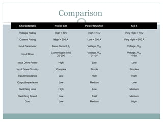
What is IGBT?
 The IGBT or Insulated Gate Bipolar Transistor is
the combination of BJT and MOSFET.
 Its name also implies the fusion between them.
“Insulated Gate” refers to the input part of MOSFET
having very high input impedance.
 It does not draw any input current rather it operates on
the voltage at its gate terminal.
 “Bipolar” refers to the output part of the BJT having
bipolar nature where the current flow is due to both types
of charge carriers.
 It allows it to handle very large currents and voltages
using small voltage signals.
 This hybrid combination makes the IGBT a voltage-
controlled device.
• It is a four-layer PNPN device having three PN junctions.
• It has three terminals Gate (G), Collector(C) and Emitter (E).
• The terminal’s name also implies being taken from both transistors.
• Gate terminal as it is the input part, taken from MOSFET while the
collector and emitter as they are the output, taken from the BJT.
Construction of IGBT
 IGBT is made of four layers of semiconductor to form a PNPN structure.
 The collector (C) electrode is attached to P layer while the emitter (E) is
attached between the P and N layers.
 A P+ substrate is used for the construction of IGBT. An N- layer is placed
on top of it to form PN junction J1.
 Two P regions are fabricated on top of N- layer to form PN junction J2.
 The P region is designed in such a way to leave a path in the middle for
the gate (G) electrode
 N+ regions are diffused over the P region as shown in the figure.
 The emitter and gate are metal electrodes
 . The emitter is directly attached to the N+ region while the gate is insulated
using a silicon dioxide layer.
 The base P+ layer inject holes into N- layer that is why it is called injector
layer.
 While the N- layer is called the drift region. Its thickness is proportional to
voltage blocking capacity. The P layer above is known as the body of IGBT.
Working of IGBT
• The two terminals of IGBT collector (C) and emitter (E) are used for the
conduction of current while the gate (G) is used for controlling the IGBT.
• Its working is based on the biasing between Gate-Emitter terminals and
Collector-Emitter terminals.
 The collector-emitter is connected to Vcc such that
the collector is kept at a positive voltage than the
emitter.
 The junction j1 becomes forward biased and j2
becomes reverse biased. At this point, there is no
voltage at the gate.
 Due to reverse j2, the IGBT remains switched off and
no current will flow between collector and emitter.
 Applying a gate voltage VG positive than the emitter,
negative charges will accumulate right beneath the
SiO2 layer due to capacitance.
 Increasing the VG increases the number of charges which
eventually form a layer when the VG exceeds the
threshold voltage, in the upper P-region. This layer form
N-channel that shorts N- drift region and N+ region.
 The electrons from the emitter flow from N+ region into
N- drift region. While the holes from the collector are
injected from the P+ region into the N- drift region. Due
to the excess of both electrons and holes in the drift
region, its conductivity increase and starts the
conduction of current. Hence the IGBT switches ON.
V-I Characteristics of IGBT
 Unlike BJT, IGBT is a voltage-controlled device that requires
only a small voltage at its gate to control the collector current.
 However, the gate-emitter voltage VGE needs to be greater
than the threshold voltage.
 Transfer characteristics of the IGBT show the relation of input
voltage VGE to output collector current IC. When the VGE is 0v,
there is no IC and the device remains switched off.
 When the VGE is slightly increased but remains below
threshold voltage VGET, the device remains switched off but
there is a leakage current.
 When the VGE exceeds the threshold limit, the IC starts to
increase and the device switches ON.
 Since it is a unidirectional device, the current only flows in one
direction.
• The given graph shows the relation between the collector
current IC and collector-emitter voltage VCE at different levels
of VGE. At VGE < VGET the IGBT is in cutoff mode and the IC =
0 at any VCE. At VGE > VGET, the IGBT goes into active mode,
where the IC increases with an increase in VCE.
• Furthermore, for each VGE where VGE1 < VGE2 < VGE3, the IC is
different.
 The reverse voltage should not exceed the reverse
breakdown limit. So does the forward voltage. If they
exceed their respective breakdown limit,
uncontrolled current starts passing through it.

 Advantages
 IGBT as a whole has the advantages of both BJT and MOSFET.
 It has higher voltage and current handling capabilities.
 It has a very high input impedance.
 It can switch very high currents using very low voltage.
 It is voltage-controlled i.e. it has no input current and low input
losses.
 The gate drive circuitry is simple and cheap.
 It can be easily switched ON by applying positive voltage and OFF
by applying zero or slightly negative voltage.
 It has very low ON-state resistance
 It has a high current density, enabling it to have a smaller chip size.
 It has a higher power gain than both BJT and MOSFET.
 It has a higher switching speed than BJT.
Disadvantages
 It has a lower switching speed than MOSFET.
 It is unidirectional it cannot conduct in reverse.
 It cannot block higher reverse voltage.
 It is costlier than BJT and MOSFET.
 It has latching problems due to the PNPN structure resembling
thyristor.
Applications of IGBT
 IGBTs have numerous applications used in AC as well as DC circuits.
Here are some of the important applications of IGBT
 It is used in SMPS (Switched Mode Power Supply) to supply power to
sensitive medical equipment and computers.
 It is used in UPS (Uninterruptible Power Supply) system.
 It is used in AC and DC motor drives offering speed control.
 It is used in chopper and inverters.
 It is used in solar inverters.
Comparison
Characteristic Power BJT Power MOSFET IGBT
Voltage Rating High < 1kV High < 1kV Very High > 1kV
Current Rating High < 500 A Low < 200 A Very High > 500 A
Input Parameter Base Current, Ib Voltage, VGS Voltage, VGE
Input Drive
Current gain (hfe)
20-200
Voltage, VGS
3-10V
Voltage, VGE
4-8V
Input Drive Power High Low Low
Input Drive Circuitry Complex Simple Simples
Input Impedance Low High High
Output Impedance Low Medium Low
Switching Loss High Low Medium
Switching Speed Low Fast Medium
Cost Low Medium High
IGBT circuit diagram.pptx

IGBT circuit diagram.pptx

  • 1.
    What is IGBT? The IGBT or Insulated Gate Bipolar Transistor is the combination of BJT and MOSFET.  Its name also implies the fusion between them. “Insulated Gate” refers to the input part of MOSFET having very high input impedance.  It does not draw any input current rather it operates on the voltage at its gate terminal.  “Bipolar” refers to the output part of the BJT having bipolar nature where the current flow is due to both types of charge carriers.  It allows it to handle very large currents and voltages using small voltage signals.  This hybrid combination makes the IGBT a voltage- controlled device.
  • 2.
    • It isa four-layer PNPN device having three PN junctions. • It has three terminals Gate (G), Collector(C) and Emitter (E). • The terminal’s name also implies being taken from both transistors. • Gate terminal as it is the input part, taken from MOSFET while the collector and emitter as they are the output, taken from the BJT.
  • 3.
    Construction of IGBT IGBT is made of four layers of semiconductor to form a PNPN structure.  The collector (C) electrode is attached to P layer while the emitter (E) is attached between the P and N layers.  A P+ substrate is used for the construction of IGBT. An N- layer is placed on top of it to form PN junction J1.  Two P regions are fabricated on top of N- layer to form PN junction J2.  The P region is designed in such a way to leave a path in the middle for the gate (G) electrode  N+ regions are diffused over the P region as shown in the figure.
  • 4.
     The emitterand gate are metal electrodes  . The emitter is directly attached to the N+ region while the gate is insulated using a silicon dioxide layer.  The base P+ layer inject holes into N- layer that is why it is called injector layer.  While the N- layer is called the drift region. Its thickness is proportional to voltage blocking capacity. The P layer above is known as the body of IGBT.
  • 5.
    Working of IGBT •The two terminals of IGBT collector (C) and emitter (E) are used for the conduction of current while the gate (G) is used for controlling the IGBT. • Its working is based on the biasing between Gate-Emitter terminals and Collector-Emitter terminals.
  • 6.
     The collector-emitteris connected to Vcc such that the collector is kept at a positive voltage than the emitter.  The junction j1 becomes forward biased and j2 becomes reverse biased. At this point, there is no voltage at the gate.  Due to reverse j2, the IGBT remains switched off and no current will flow between collector and emitter.  Applying a gate voltage VG positive than the emitter, negative charges will accumulate right beneath the SiO2 layer due to capacitance.
  • 7.
     Increasing theVG increases the number of charges which eventually form a layer when the VG exceeds the threshold voltage, in the upper P-region. This layer form N-channel that shorts N- drift region and N+ region.  The electrons from the emitter flow from N+ region into N- drift region. While the holes from the collector are injected from the P+ region into the N- drift region. Due to the excess of both electrons and holes in the drift region, its conductivity increase and starts the conduction of current. Hence the IGBT switches ON.
  • 8.
    V-I Characteristics ofIGBT  Unlike BJT, IGBT is a voltage-controlled device that requires only a small voltage at its gate to control the collector current.  However, the gate-emitter voltage VGE needs to be greater than the threshold voltage.  Transfer characteristics of the IGBT show the relation of input voltage VGE to output collector current IC. When the VGE is 0v, there is no IC and the device remains switched off.  When the VGE is slightly increased but remains below threshold voltage VGET, the device remains switched off but there is a leakage current.  When the VGE exceeds the threshold limit, the IC starts to increase and the device switches ON.  Since it is a unidirectional device, the current only flows in one direction.
  • 9.
    • The givengraph shows the relation between the collector current IC and collector-emitter voltage VCE at different levels of VGE. At VGE < VGET the IGBT is in cutoff mode and the IC = 0 at any VCE. At VGE > VGET, the IGBT goes into active mode, where the IC increases with an increase in VCE. • Furthermore, for each VGE where VGE1 < VGE2 < VGE3, the IC is different.
  • 10.
     The reversevoltage should not exceed the reverse breakdown limit. So does the forward voltage. If they exceed their respective breakdown limit, uncontrolled current starts passing through it. 
  • 11.
     Advantages  IGBTas a whole has the advantages of both BJT and MOSFET.  It has higher voltage and current handling capabilities.  It has a very high input impedance.  It can switch very high currents using very low voltage.  It is voltage-controlled i.e. it has no input current and low input losses.  The gate drive circuitry is simple and cheap.  It can be easily switched ON by applying positive voltage and OFF by applying zero or slightly negative voltage.  It has very low ON-state resistance  It has a high current density, enabling it to have a smaller chip size.  It has a higher power gain than both BJT and MOSFET.  It has a higher switching speed than BJT.
  • 12.
    Disadvantages  It hasa lower switching speed than MOSFET.  It is unidirectional it cannot conduct in reverse.  It cannot block higher reverse voltage.  It is costlier than BJT and MOSFET.  It has latching problems due to the PNPN structure resembling thyristor. Applications of IGBT  IGBTs have numerous applications used in AC as well as DC circuits. Here are some of the important applications of IGBT  It is used in SMPS (Switched Mode Power Supply) to supply power to sensitive medical equipment and computers.  It is used in UPS (Uninterruptible Power Supply) system.  It is used in AC and DC motor drives offering speed control.  It is used in chopper and inverters.  It is used in solar inverters.
  • 13.
    Comparison Characteristic Power BJTPower MOSFET IGBT Voltage Rating High < 1kV High < 1kV Very High > 1kV Current Rating High < 500 A Low < 200 A Very High > 500 A Input Parameter Base Current, Ib Voltage, VGS Voltage, VGE Input Drive Current gain (hfe) 20-200 Voltage, VGS 3-10V Voltage, VGE 4-8V Input Drive Power High Low Low Input Drive Circuitry Complex Simple Simples Input Impedance Low High High Output Impedance Low Medium Low Switching Loss High Low Medium Switching Speed Low Fast Medium Cost Low Medium High