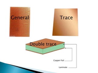
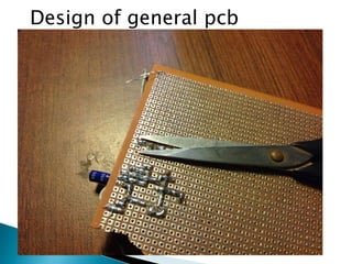
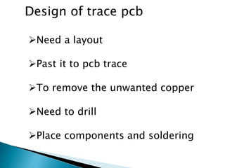
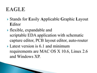
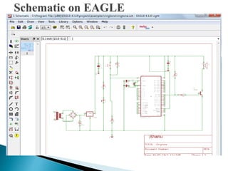
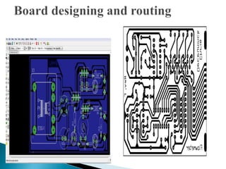
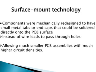
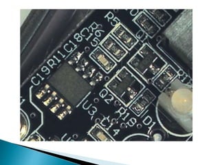
By
G.SIVA
13A81A0472
E.C.E-B
INTRODUCTION
WHAT IS PCB?
WHAT IS THE NEED OF PCB?
TYPES OF PCB
DESIGN OF TRACE PCB
ADVANTAGES
DIS ADVANTAGES
APPLICATIONS
 A printed circuit board (PCB) mechanically
supports and electrically connects electronic
components using conductive tracks, pads and other
features etched from copper sheets laminated onto a
non-conductive substrate.
 FR-4 glass epoxy is the primary insulating
substrate upon which the vast majority of
rigid PCBs are produced.
 A PCB populated with electronic components is
called a printed circuit assembly (PCA), printed
circuit board assembly or PCB assembly (PCBA)
To make a permanent circuit
To avoid short circuit
To avoid wires
To reduce the cost of circuit
To reduce the size of circuit
To reuse the pcb design
Need of pcb
Types of pcb
General pcb
Trace pcb
Single layer pcb
Double layer pcb
General Trace
Copper Foil
Laminate
Double trace
Design of general pcb
Design of trace pcb
Need a layout
Past it to pcb trace
To remove the unwanted copper
Need to drill
Place components and soldering
 Stands for Easily Applicable Graphic Layout
Editor
 flexible, expandable and
scriptable EDA application with schematic
capture editor, PCB layout editor, auto-router
 Latest version is 6.1 and minimum
requirements are MAC OS X 10.6, Linux 2.6
and Windows XP.
Chemical etching
Chemical etching is usually done with
ammonium per sulfate or ferric chloride.
 In which the board is submerged in etching
solution such as ferric chloride
Solution
 The etching time is long. Heat and agitation can
be applied to the bath to speed the etching rate.
Surface-mount technology
Components were mechanically redesigned to have
small metal tabs or end caps that could be soldered
directly onto the PCB surface
Instead of wire leads to pass through holes
Allowing much smaller PCB assemblies with much
higher circuit densities.
 The circuit board fabrication cost (pcb cost) is lower with
mass quantity production.
Chances of miss wiring or short-circuited wiring are
minimized.
Component wiring and assembly can be minimized in a
circuit board manufacturing facility.
The location of electronic parts is fixed and so it
simplifies components identification and maintenance of
equipment.
Advantages
Re designing is required for the new type
of circuit operation.
Very hard to get repaired if it gets
damaged.
 We can not update it , once printed.
 Etching of this PCB generates chemicals
which are the harmful for the
environment.....
Disadvantages
pcb

pcb

  • 1.
  • 2.
    INTRODUCTION WHAT IS PCB? WHATIS THE NEED OF PCB? TYPES OF PCB DESIGN OF TRACE PCB ADVANTAGES DIS ADVANTAGES APPLICATIONS
  • 3.
     A printedcircuit board (PCB) mechanically supports and electrically connects electronic components using conductive tracks, pads and other features etched from copper sheets laminated onto a non-conductive substrate.  FR-4 glass epoxy is the primary insulating substrate upon which the vast majority of rigid PCBs are produced.  A PCB populated with electronic components is called a printed circuit assembly (PCA), printed circuit board assembly or PCB assembly (PCBA)
  • 4.
    To make apermanent circuit To avoid short circuit To avoid wires To reduce the cost of circuit To reduce the size of circuit To reuse the pcb design Need of pcb
  • 5.
    Types of pcb Generalpcb Trace pcb Single layer pcb Double layer pcb
  • 6.
  • 7.
  • 8.
    Design of tracepcb Need a layout Past it to pcb trace To remove the unwanted copper Need to drill Place components and soldering
  • 9.
     Stands forEasily Applicable Graphic Layout Editor  flexible, expandable and scriptable EDA application with schematic capture editor, PCB layout editor, auto-router  Latest version is 6.1 and minimum requirements are MAC OS X 10.6, Linux 2.6 and Windows XP.
  • 13.
    Chemical etching Chemical etchingis usually done with ammonium per sulfate or ferric chloride.  In which the board is submerged in etching solution such as ferric chloride Solution  The etching time is long. Heat and agitation can be applied to the bath to speed the etching rate.
  • 16.
    Surface-mount technology Components weremechanically redesigned to have small metal tabs or end caps that could be soldered directly onto the PCB surface Instead of wire leads to pass through holes Allowing much smaller PCB assemblies with much higher circuit densities.
  • 18.
     The circuitboard fabrication cost (pcb cost) is lower with mass quantity production. Chances of miss wiring or short-circuited wiring are minimized. Component wiring and assembly can be minimized in a circuit board manufacturing facility. The location of electronic parts is fixed and so it simplifies components identification and maintenance of equipment. Advantages
  • 19.
    Re designing isrequired for the new type of circuit operation. Very hard to get repaired if it gets damaged.  We can not update it , once printed.  Etching of this PCB generates chemicals which are the harmful for the environment..... Disadvantages