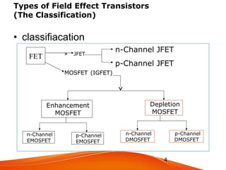
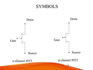
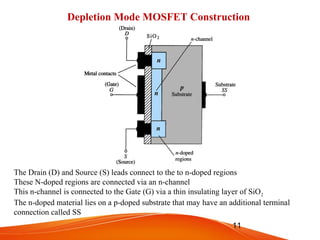
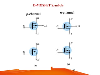
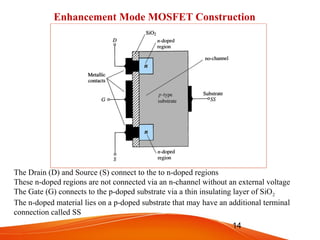
1
Field Effect Transistor (FET)
Mr.Nikunj Bhensdadiya
(lecturer - Electrical Dept.)
Kalyan Polytechnic - jamnagar
2
What is FET?
FET is uni-polar device i.e.
operation depends on only one type
of charge carriers (h or e) . It is a
Voltage controlled Device (gate
voltage controls drain current)
3
Current Controlled vs Voltage Controlled
Devices
4
Types of Field Effect Transistors
(The Classification)
n-Channel JFET
p-Channel JFET
n-Channel
EMOSFET
p-Channel
EMOSFET
Enhancement
MOSFET
Depletion
MOSFET
n-Channel
DMOSFET
p-Channel
DMOSFET
FETFETFET » JFET
MOSFET (IGFET)
FET » JFET
MOSFET (IGFET)
FET
• classifiacation
5
JFET Construction
There are two types of JFET’s: n-channel and p-channel.
The n-channel is more widely used.
There are three terminals: Drain (D) and Source (S) are connected to n-channel
Gate (G) is connected to the p-type material
6
The nonconductive depletion region becomes thicker with increased reverse bias.
(Note: The two gate regions of each FET are connected to each other.)
N-Channel JFET Operation
7
Gate
Drain
Source
SYMBOLS
n-channel JFET
Gate
Drain
Source
p-channel JFET
8
p-Channel JFET
p-Channel JFET operates in a similar manner as the n-channel JFET except the voltage
polarities and current directions are reversed
9
MOSFET
(Metal Oxide Semiconductor FET)
10
MOSFET
There are two types of MOSFET’s:
• Depletion mode MOSFET (D-MOSFET)
• Operates in Depletion mode the same way as a JFET
when VGS ≤ 0
• Operates in Enhancement mode like E-MOSFET when
VGS > 0
• Enhancement Mode MOSFET (E-MOSFET)
• Operates in Enhancement mode
• IDSS = 0 until VGS > VT (threshold voltage)
11
Depletion Mode MOSFET Construction
The Drain (D) and Source (S) leads connect to the to n-doped regions
These N-doped regions are connected via an n-channel
This n-channel is connected to the Gate (G) via a thin insulating layer of SiO2
The n-doped material lies on a p-doped substrate that may have an additional terminal
connection called SS
12
D-MOSFET Symbols
13
Enhancement Mode
MOSFET’s
14
Enhancement Mode MOSFET Construction
The Drain (D) and Source (S) connect to the to n-doped regions
These n-doped regions are not connected via an n-channel without an external voltage
The Gate (G) connects to the p-doped substrate via a thin insulating layer of SiO2
The n-doped material lies on a p-doped substrate that may have an additional terminal
connection called SS
15
E-MOSFET Symbols
16

FET FOR DIPLOMA

  • 1.
    1 Field Effect Transistor(FET) Mr.Nikunj Bhensdadiya (lecturer - Electrical Dept.) Kalyan Polytechnic - jamnagar
  • 2.
    2 What is FET? FETis uni-polar device i.e. operation depends on only one type of charge carriers (h or e) . It is a Voltage controlled Device (gate voltage controls drain current)
  • 3.
    3 Current Controlled vsVoltage Controlled Devices
  • 4.
    4 Types of FieldEffect Transistors (The Classification) n-Channel JFET p-Channel JFET n-Channel EMOSFET p-Channel EMOSFET Enhancement MOSFET Depletion MOSFET n-Channel DMOSFET p-Channel DMOSFET FETFETFET » JFET MOSFET (IGFET) FET » JFET MOSFET (IGFET) FET • classifiacation
  • 5.
    5 JFET Construction There aretwo types of JFET’s: n-channel and p-channel. The n-channel is more widely used. There are three terminals: Drain (D) and Source (S) are connected to n-channel Gate (G) is connected to the p-type material
  • 6.
    6 The nonconductive depletionregion becomes thicker with increased reverse bias. (Note: The two gate regions of each FET are connected to each other.) N-Channel JFET Operation
  • 7.
  • 8.
    8 p-Channel JFET p-Channel JFEToperates in a similar manner as the n-channel JFET except the voltage polarities and current directions are reversed
  • 9.
  • 10.
    10 MOSFET There are twotypes of MOSFET’s: • Depletion mode MOSFET (D-MOSFET) • Operates in Depletion mode the same way as a JFET when VGS ≤ 0 • Operates in Enhancement mode like E-MOSFET when VGS > 0 • Enhancement Mode MOSFET (E-MOSFET) • Operates in Enhancement mode • IDSS = 0 until VGS > VT (threshold voltage)
  • 11.
    11 Depletion Mode MOSFETConstruction The Drain (D) and Source (S) leads connect to the to n-doped regions These N-doped regions are connected via an n-channel This n-channel is connected to the Gate (G) via a thin insulating layer of SiO2 The n-doped material lies on a p-doped substrate that may have an additional terminal connection called SS
  • 12.
  • 13.
  • 14.
    14 Enhancement Mode MOSFETConstruction The Drain (D) and Source (S) connect to the to n-doped regions These n-doped regions are not connected via an n-channel without an external voltage The Gate (G) connects to the p-doped substrate via a thin insulating layer of SiO2 The n-doped material lies on a p-doped substrate that may have an additional terminal connection called SS
  • 15.
  • 16.