transistor is a swithe og electrronis so we can make it control
1.
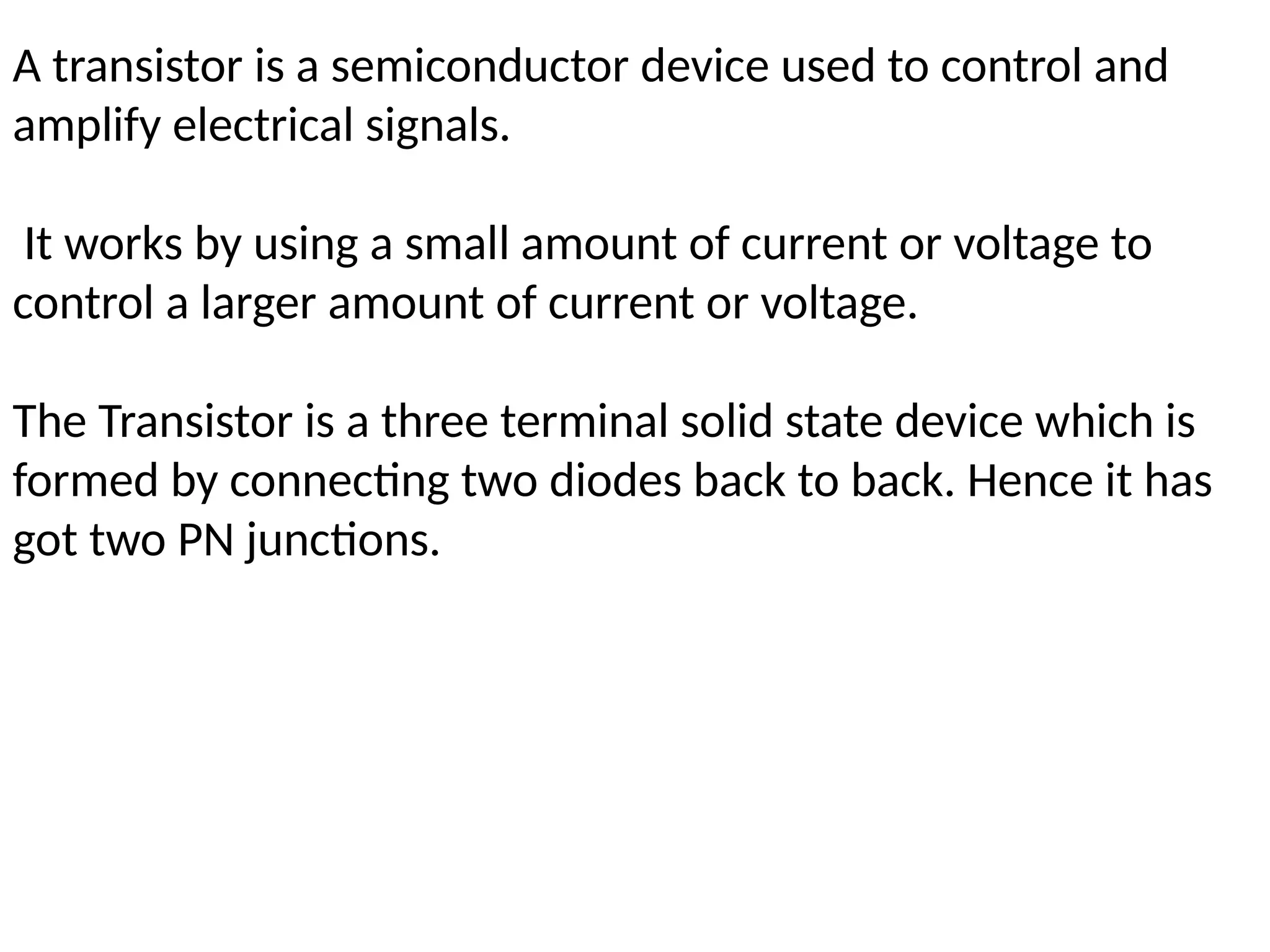
A transistor isa semiconductor device used to control and
amplify electrical signals.
It works by using a small amount of current or voltage to
control a larger amount of current or voltage.
The Transistor is a three terminal solid state device which is
formed by connecting two diodes back to back. Hence it has
got two PN junctions.
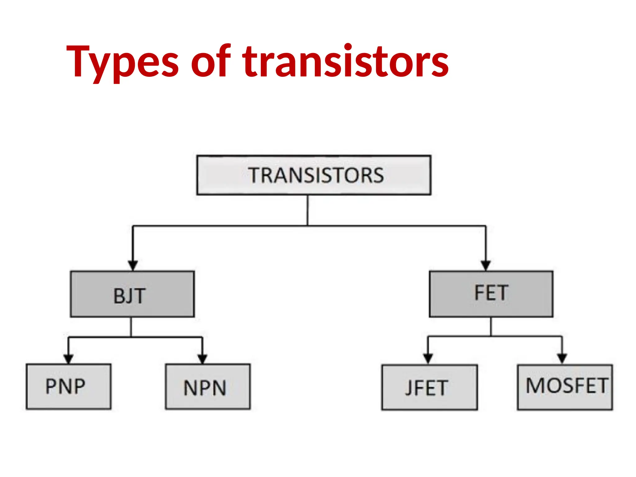
Constructional and workingprinciples of BJT
BJT is a three terminal semiconductor materials .
They are PNP and NPN which means an N-type material between two Ptypes and the
other is a P-type material between two N-types respectively.
When a voltage is applied to the base-emitter junction, current flows from the base to
the emitter, and electrons are injected from the base into the emitter
the PN junction between the base and emitter becomes forward biased
large electrons flow from the emitter to the base, some electrons flow out of the base
terminal.
the p-type semiconductor is very thin, the electrons from the emitter on entering the
base terminal immediately jump to the collector region.
current flows from the collector to the emitter which is grounded for an NPN
transistor
For a PNP current flows from the emitter to the collector. The collector is grounded.
4.
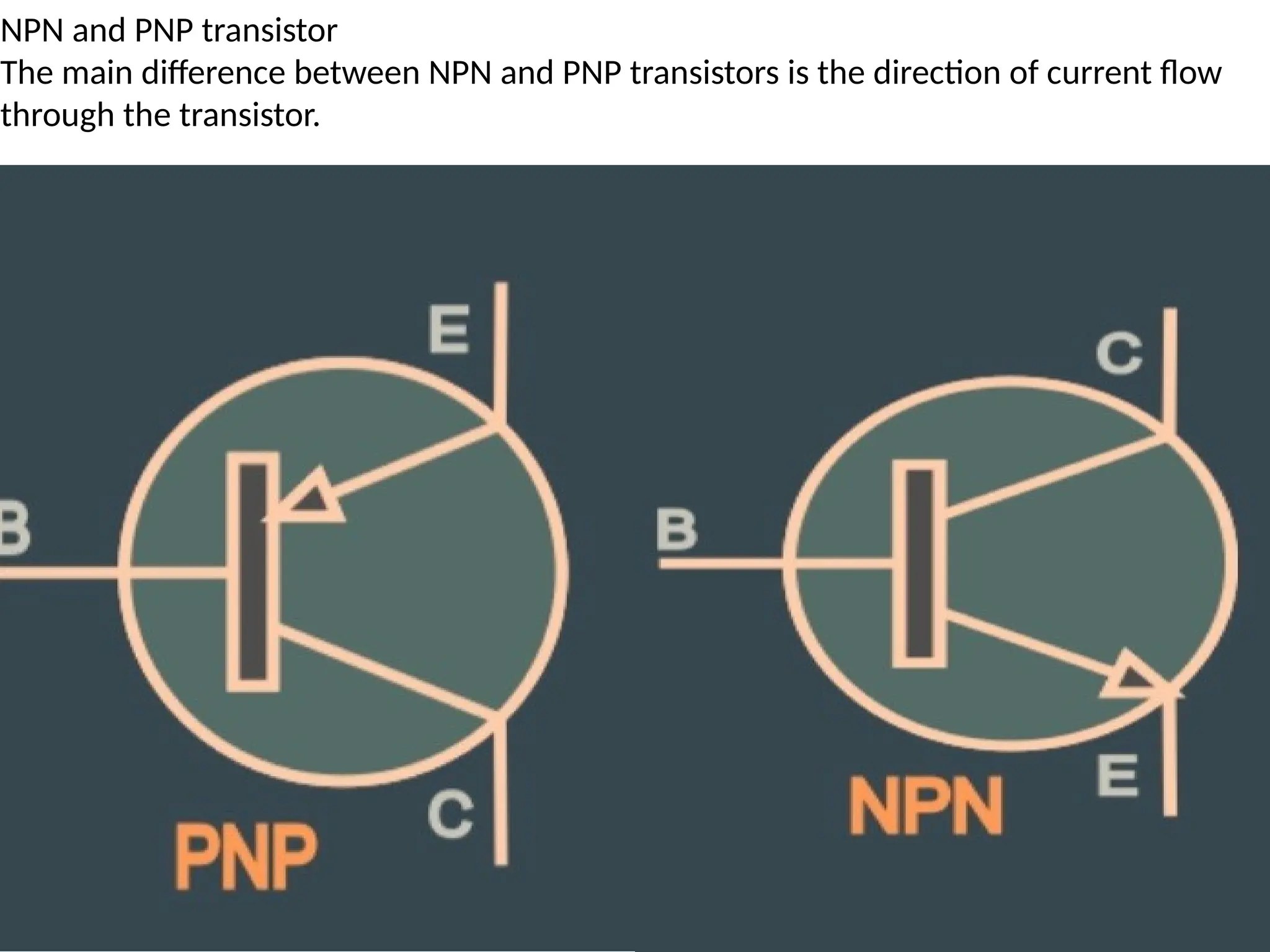
NPN and PNPtransistor
The main difference between NPN and PNP transistors is the direction of current flow
through the transistor.
7.
Field Effect Transistor(FET)
FET is a unipolar semiconductor device.
FETS are three-terminal semiconductor devices that consist of a
source, a gate, and a drain.
It is a voltage controlled device
The FET is a unipolar device, which means that it is made using
either p-type or n-type material as main substrate.
current conduction of a FET is done by either electrons or holes.
electric field to control the flow of current between the source
and drain terminals.
8.
FET working principles
Thesource and drain are normally connected to a voltage source and
the gate is connected to an electrode or control voltage.
When a voltage is applied to the gate, this creates an electric field in
the channel between the source and the drain. This electric field then
modifies the conductivity of
the channel, controlling the current flow between the
SOurce and the drain.
10.
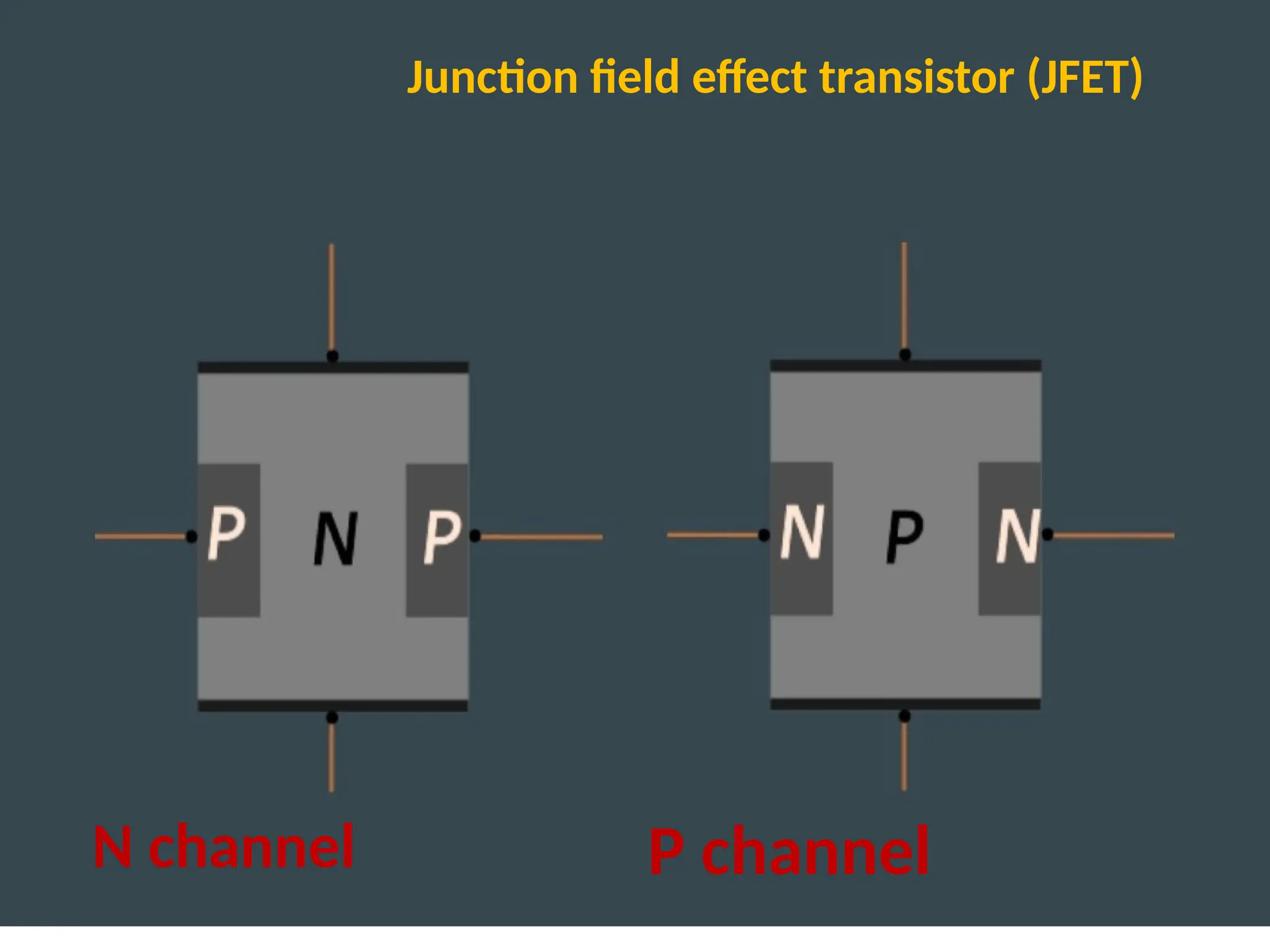
JFET(junction field effecttransistor)
jfet are typically made from a single semiconductor material, such as silicon, and
have a very simple construction.
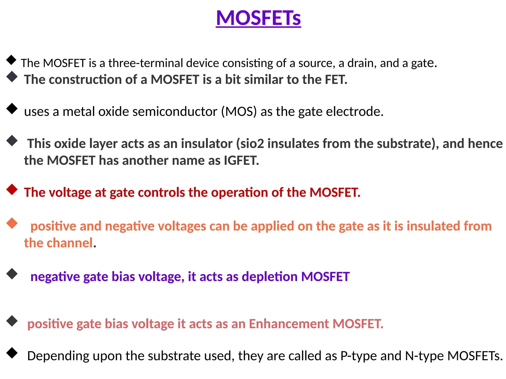
MOSFETs
The MOSFETis a three-terminal device consisting of a source, a drain, and a gate.
The construction of a MOSFET is a bit similar to the FET.
uses a metal oxide semiconductor (MOS) as the gate electrode.
This oxide layer acts as an insulator (sio2 insulates from the substrate), and hence
the MOSFET has another name as IGFET.
The voltage at gate controls the operation of the MOSFET.
positive and negative voltages can be applied on the gate as it is insulated from
the channel.
negative gate bias voltage, it acts as depletion MOSFET
positive gate bias voltage it acts as an Enhancement MOSFET.
Depending upon the substrate used, they are called as P-type and N-type MOSFETs.
14.
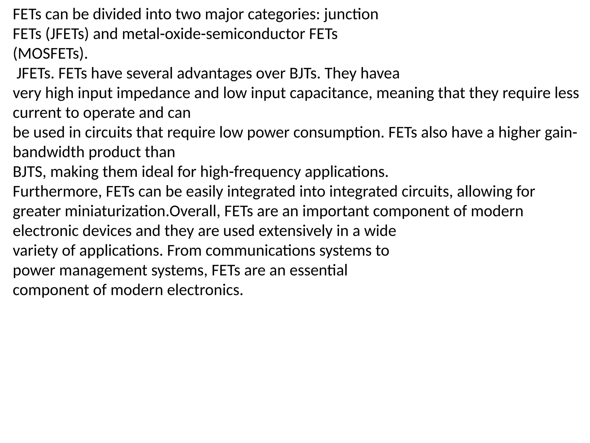
FETs can bedivided into two major categories: junction
FETs (JFETs) and metal-oxide-semiconductor FETs
(MOSFETs).
JFETs. FETs have several advantages over BJTs. They havea
very high input impedance and low input capacitance, meaning that they require less
current to operate and can
be used in circuits that require low power consumption. FETs also have a higher gain-
bandwidth product than
BJTS, making them ideal for high-frequency applications.
Furthermore, FETs can be easily integrated into integrated circuits, allowing for
greater miniaturization.Overall, FETs are an important component of modern
electronic devices and they are used extensively in a wide
variety of applications. From communications systems to
power management systems, FETs are an essential
component of modern electronics.
15.
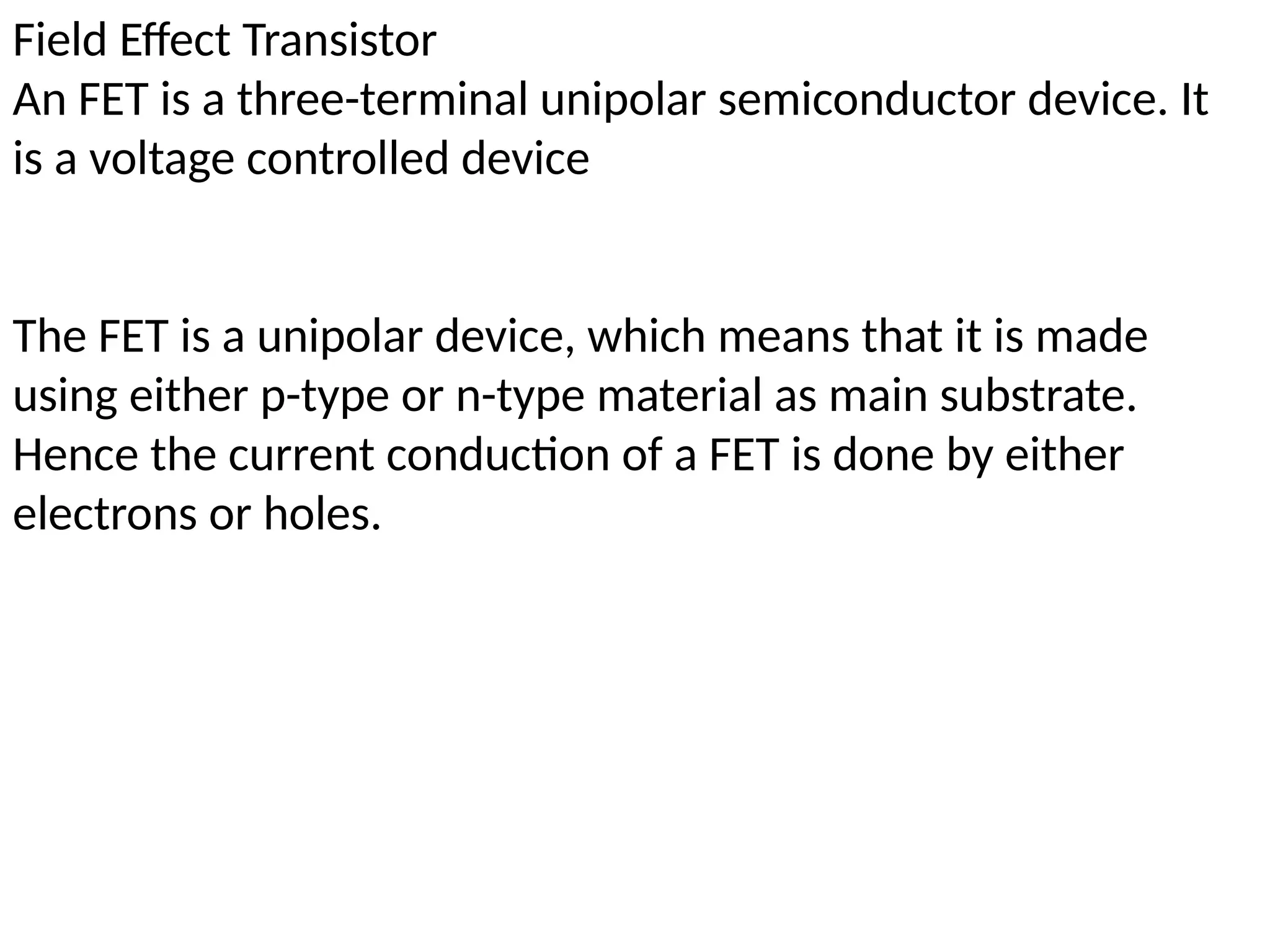
Field Effect Transistor
AnFET is a three-terminal unipolar semiconductor device. It
is a voltage controlled device
The FET is a unipolar device, which means that it is made
using either p-type or n-type material as main substrate.
Hence the current conduction of a FET is done by either
electrons or holes.
16.
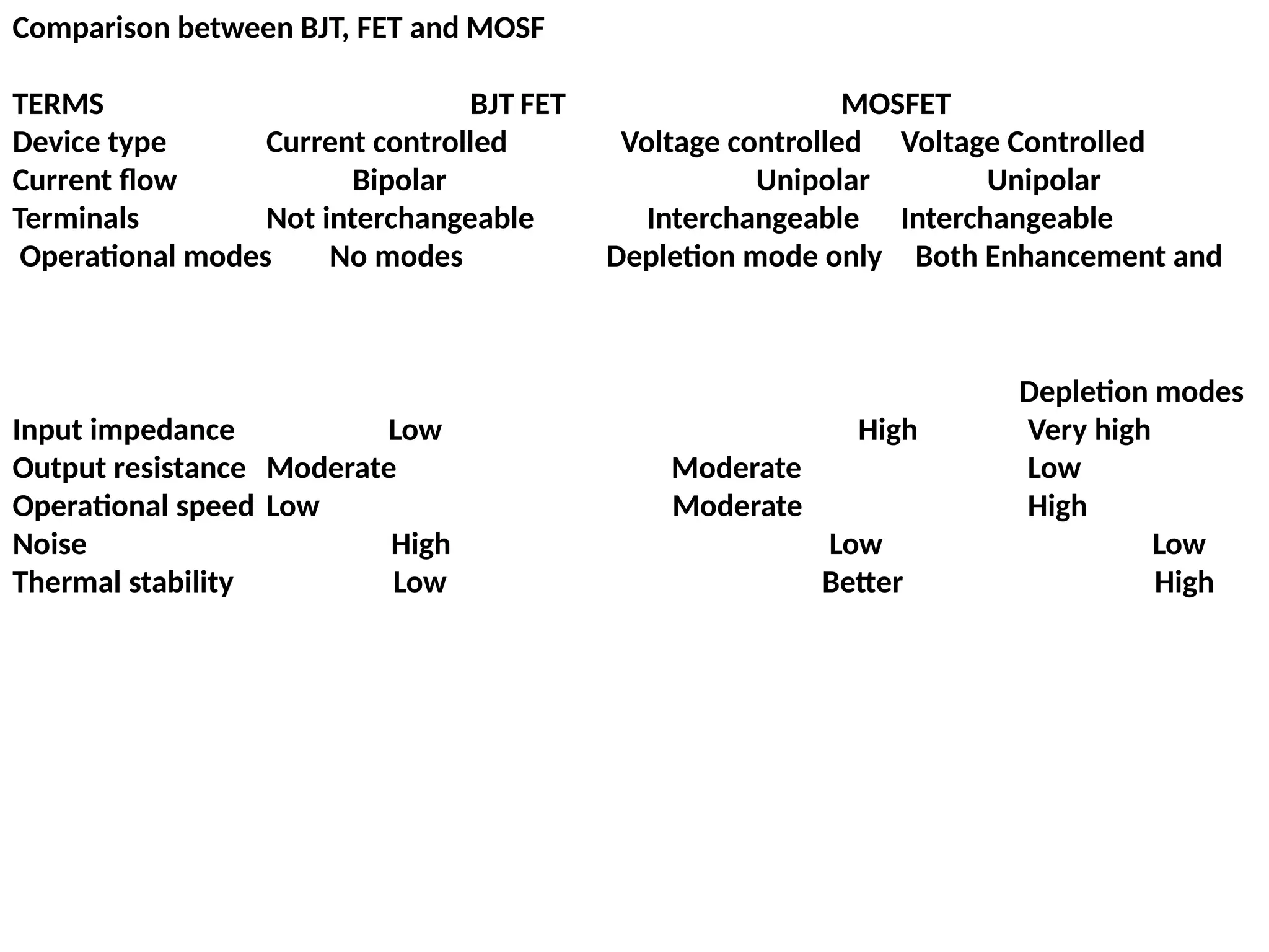
Comparison between BJT,FET and MOSF
TERMS BJT FET MOSFET
Device type Current controlled Voltage controlled Voltage Controlled
Current flow Bipolar Unipolar Unipolar
Terminals Not interchangeable Interchangeable Interchangeable
Operational modes No modes Depletion mode only Both Enhancement and
Depletion modes
Input impedance Low High Very high
Output resistance Moderate Moderate Low
Operational speed Low Moderate High
Noise High Low Low
Thermal stability Low Better High
17.
Features of FET
Thefollowing are the varied features of a Field Effect Transistor.
Unipolar − It is unipolar as either holes or electrons are responsible for
conduction.
High input impedance − The input current in a FET flows due to the
reverse bias. Hence it has high input impedance.
Voltage controlled device − As the output voltage of a FET is controlled
by the gate input voltage, FET is called as the voltage controlled
device.
Noise is low − There are no junctions present in the conduction path.
Hence noise is lower than in BJTs.
Gain is characterized as transconductance. Transconductance is the
ratio of change in output current to the change in input voltage.
18.
Bipolar Junction Transistor
ABipolar junction transistor, shortly termed as BJT is called so as it has
two PN junctions for its function. This BJT is nothing but a normal
transistor.
It has got two types of configurations NPN and PNP.
Usually NPN transistor is preferred for the sake of convenience.
The NPN transistor is made by placing a p type material between two
n-type materials.
The PNP transistor is made by placing an ntype material between two
p-type materials.
BJT is a current controlled device.
19.
Advantages of FET
Toprefer a FET over BJT, there should be few advantages of
using FETs, rather than BJTs. Let us try to summarize the
advantages of FET over BJT.
JFET BJT
It is an unipolar device It is a bipolar device
Voltage driven device Current driven device
High input impedance Low input impedance
Low noise level High noise level
Better thermal stability Less thermal stability
Gain is characterized by transconductance Gain is
characterized by voltage gain
20.
MOSFETs provide severaladvantages over other types of FETs. They are more efficient, require
less energy to operate, and have greater power handling capabilities.
Additionally, MOSFETs are more reliable and less Susceptible to damage due to electrostatic
discharge (ESD). They are also capable of operating at higher
frequencies than other types of FETs.
MOSFETs can be used in many different applications,ranging from power control to signal
amplification. They commonly used in power supplies, motor control, and audio amplifiers.
They are also used in the switching of computer memory and in the control of light-emitting
diodes.
21.
Metal oxide fieldeffect transistors (MOSFETs)
uses a metal oxide semiconductor (MOS) as the gate electrode.
MOSFETs are the most commonly used type of FET
The MOSFET is a three-terminal device
consisting of a source, a drain, and a gate.
The gate is a metal oxide layer which is placed between the source and
drain and acts as a switch by controlling the flow of current between
the two terminals.
MOSFETs operate by controlling the flow of electrons through a metal
oxide layer. When a voltage is applied to the gate, a conducting channel
is created between the source and drain.
This allows electrons to flow through the channel, creating a current
between the two terminals.
The amount of current is determined by the voltage applied to the gate,
which can then be used to control the amount of power being supplied
25.
Depletion-mode MOSFETs
A depletion-modeMOSFET (metal-oxide-semiconductor field-effect transistor) is a type of
MOSFET in which the source-channel region is pre-depleted of charge carriers.
The MOSFET is then in the off state and requires a negative gate voltage to turn it on.
The depletion-mode MOSFET works by having an n-type
channel with an n-type source and an n-type drain.
The gate of the MOSFET is connected to a negative voltage, which creates an electric field
between the gate and the source-drain region.
This electric field repels electrons away from the source-drain region, creating a depletion
region. This region is depleted of electrons and so the current between the source and drain is
blocked. In order to turn the MOSFET on, the gate voltage must be increased to a positive
voltage. This will reduce the electric field between the gate and source-drain region and allow
electrons to flow from the source to the drain. The amount of Current that can flow fromn the
source to
the drain is determined by the applied voltage and the size of the MOSFET.
The depletion-mode MOSFET İs most commonly used in power supply circuits, where the
device can be used to control the amount of current flowing through the circuit.
It is also useful in voltage-controlled oscillators and amplifiers.
26.
A lightly dopedP-type substrate is taken into which two
heavily doped N-type regions are diffused, which act as source
and drain. Between these two N+ regions, there occurs
diffusion to form an Nchannel, connecting drain and source.
27.
Enhancement-mode MOSFET
An enhancement-modeMOSFET (metal-oxide- semiconductor field-effect transistor) is a type of
transistor that is used to control Current flow between two
points in a circuit. When a voltage is applied to the gate, it creates an electric field that attracts
electrons from the source and allows them to flow to the drain.
This allows the current to flow between the source and drain, enabling the MOSFET to act as a
switch. The amount of current that can flow between the source and drain can be controlled by
varying the voltage applied to the gate.
The enhancement-mode MOSFET İs different from other types of transistors in that it does not
require a current to be passed through the gate in order for current to flow between the source
and drain. Instead, when a voltage is applied to the gate, it creates an electric field that attracts
electrons from the source and allows them to flow to the drain. This allows the current to flow
between the source and drain without the need for a current to be passed through the gate.
This makes the enhancement-mode MOSFET a more efficient and reliable type of transistor. It is
commonly used in digital circuits and other applications that require precise control of current
flow.


![Aim-to study characterstics of fet (field effect [Autosaved].pptx](https://cdn.slidesharecdn.com/ss_thumbnails/aim-tostudycharactersticsoffetfieldeffectautosaved-221113041420-4dcee974-thumbnail.jpg?width=640&height=640&fit=bounds)


