Downloaded 394 times
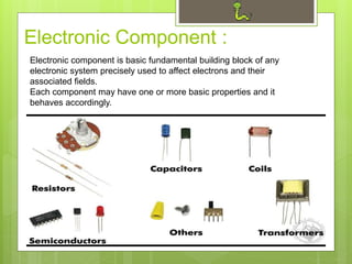
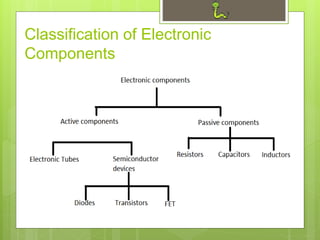
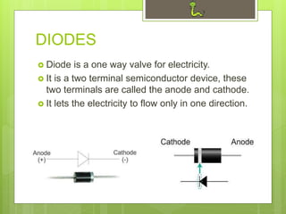
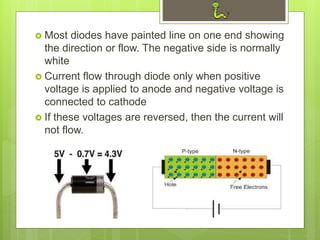
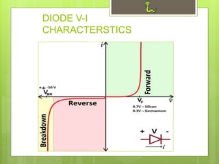
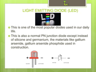


The document provides an introduction to electronic components, detailing their classifications into active components such as diodes and transistors. It discusses the functionality and applications of diodes, including light-emitting diodes (LEDs) and various types of transistors, notably field-effect transistors (FETs) and operational amplifiers (op-amps). Additionally, it highlights the IC-555 timer's uses in generating time delays and various signal applications.


