❑ Introduction
➢ FETsare unipolar devices because, unlike BJTs that use both electrons and hole
current, they operate only with one type of charge carrier.
➢ FETs is a three terminal device used for a variety of applications that much ,to
the large extent, those of the BJT transistor.
➢ The 1st FET was invented in 1926 by Jwlius edger (Lilien fred and by Oskar Hiel
in 1934).
➢ MOSFET was invented by D.Kahg in 1959.
➢ In “ Field Effect” transistors an electric field is developed by the charges
presents.
➢This electric field control the conduction path of the output circuit without the
need for direct contact between the controlling and controlled quantities.
3.
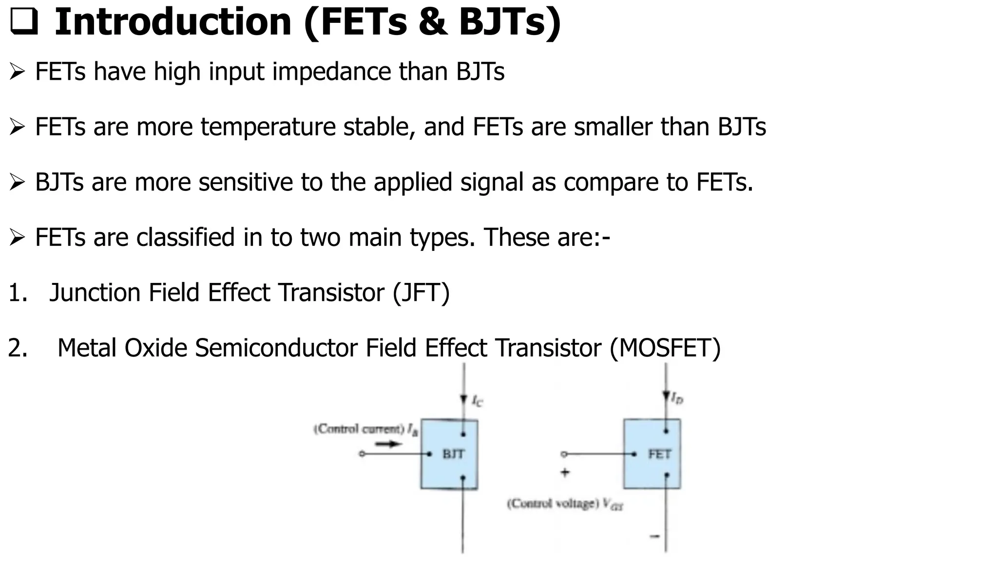
❑ Introduction (FETs& BJTs)
➢ FETs have high input impedance than BJTs
➢ FETs are more temperature stable, and FETs are smaller than BJTs
➢ BJTs are more sensitive to the applied signal as compare to FETs.
➢ FETs are classified in to two main types. These are:-
1. Junction Field Effect Transistor (JFT)
2. Metal Oxide Semiconductor Field Effect Transistor (MOSFET)
4.
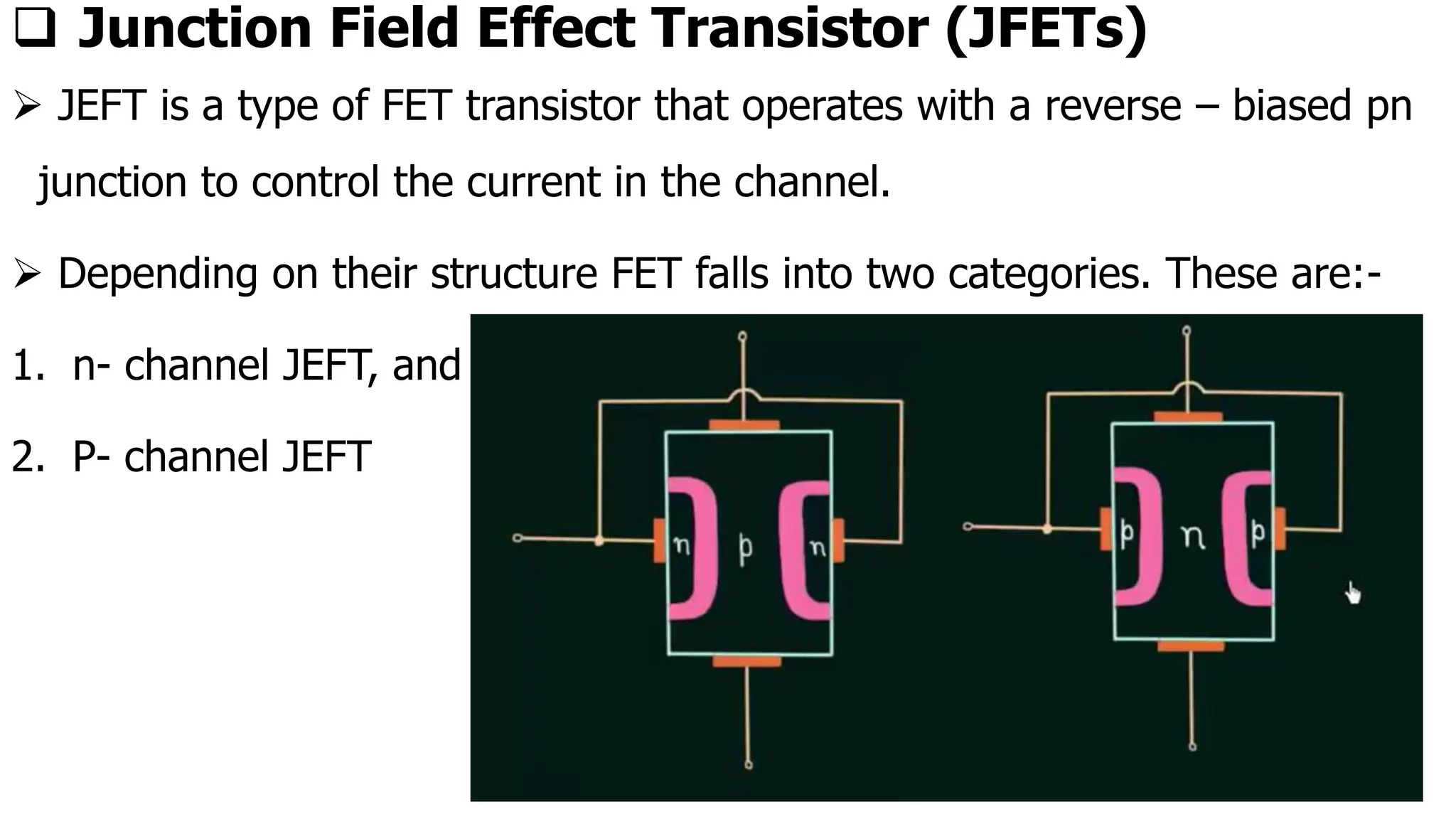
❑ Junction FieldEffect Transistor (JFETs)
➢ JEFT is a type of FET transistor that operates with a reverse – biased pn
junction to control the current in the channel.
➢ Depending on their structure FET falls into two categories. These are:-
1. n- channel JEFT, and
2. P- channel JEFT
5.
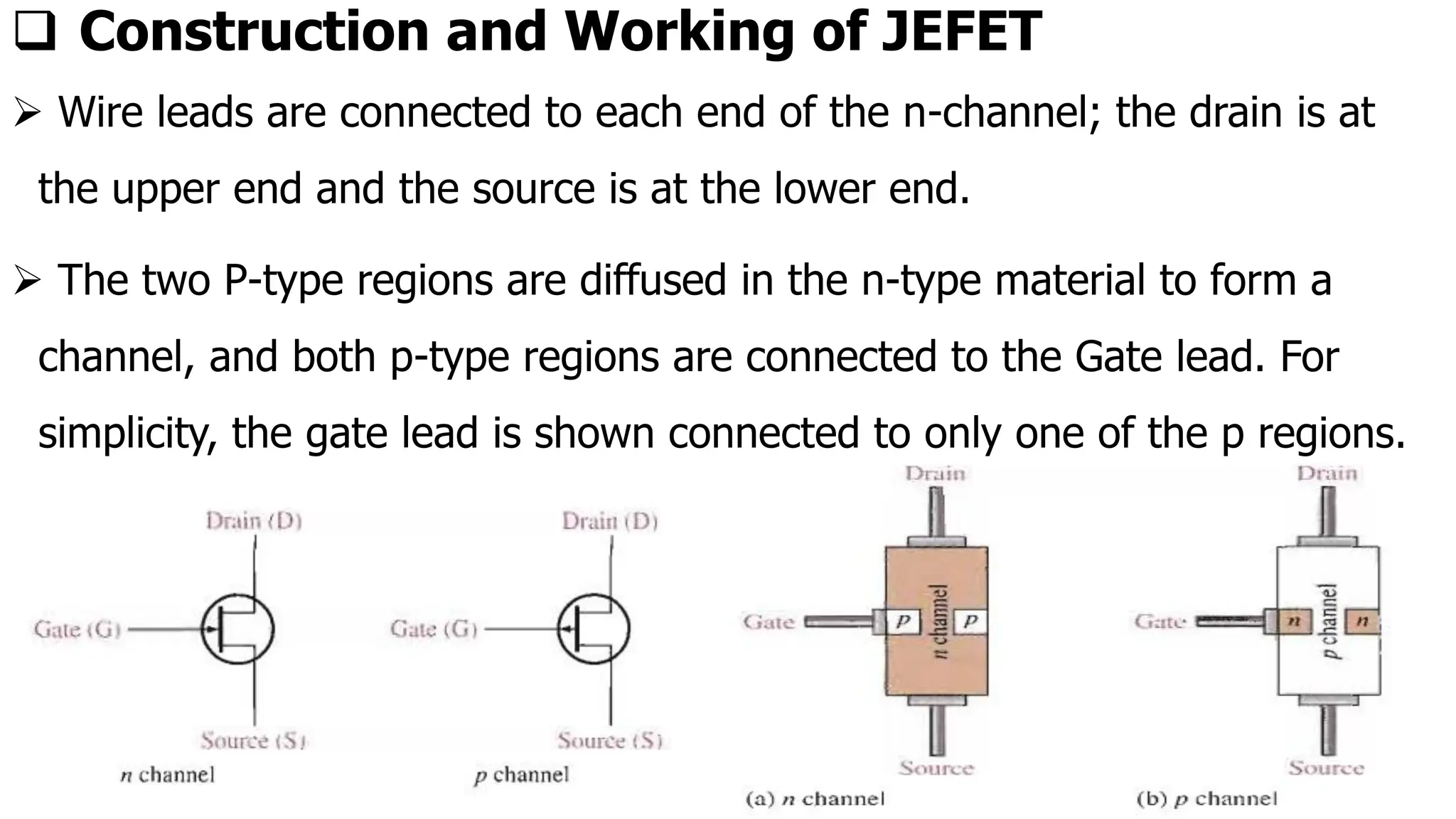
❑ Construction andWorking of JEFET
➢ Wire leads are connected to each end of the n-channel; the drain is at
the upper end and the source is at the lower end.
➢ The two P-type regions are diffused in the n-type material to form a
channel, and both p-type regions are connected to the Gate lead. For
simplicity, the gate lead is shown connected to only one of the p regions.
6.
❑ Construction andWorking of JEFET
➢ In case of n-channel JFET, the major part of FET is n-type material.
➢ It formed a channel between embedded two p-type material.
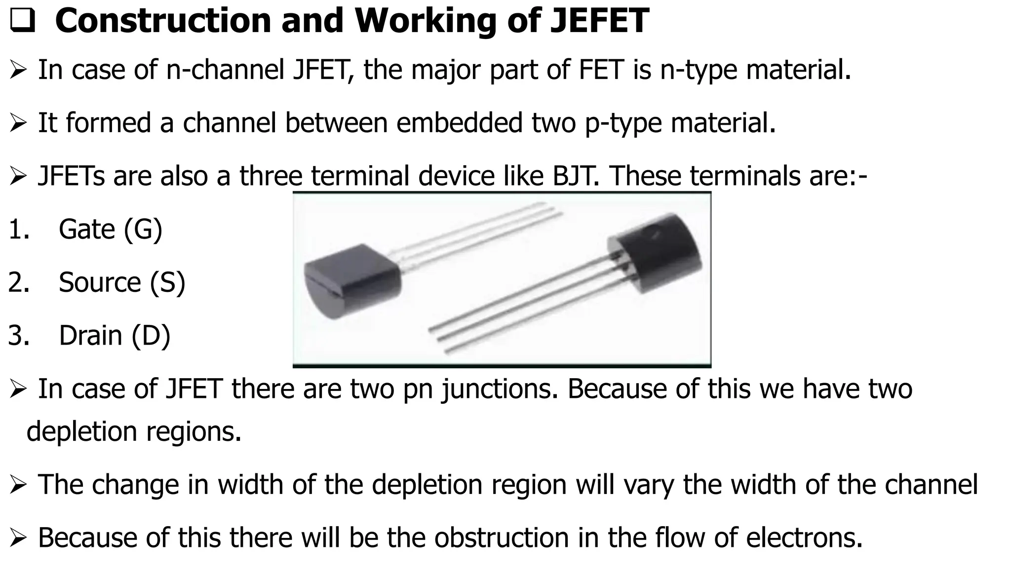
➢ JFETs are also a three terminal device like BJT. These terminals are:-
1. Gate (G)
2. Source (S)
3. Drain (D)
➢ In case of JFET there are two pn junctions. Because of this we have two
depletion regions.
➢ The change in width of the depletion region will vary the width of the channel
➢ Because of this there will be the obstruction in the flow of electrons.
7.
❑ Construction andWorking of JEFET
➢ When we connect drain and source terminals to external voltage source,
it drifts the free charge carriers (electrons or holes) in the channel.
➢ We can control the width of the depletion region by using gate(G).Which
enables to us to control the flow of electrons by using gate terminal.
➢ The potential difference between gate (G) and source (S) terminal (𝑉𝐺𝑆)
will control the width of depletion region.
➢ 𝑉𝐺𝑆 can control the output current 𝐼𝐷. Because of this we called this
device Voltage Controlled.
8.
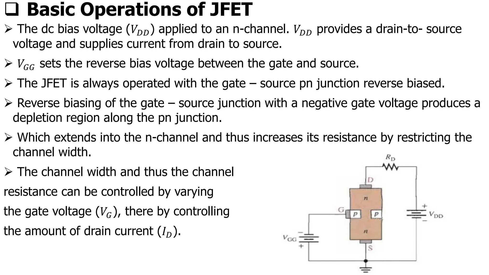
❑ Basic Operationsof JFET
➢ The dc bias voltage (𝑉𝐷𝐷) applied to an n-channel. 𝑉𝐷𝐷 provides a drain-to- source
voltage and supplies current from drain to source.
➢ 𝑉𝐺𝐺 sets the reverse bias voltage between the gate and source.
➢ The JFET is always operated with the gate – source pn junction reverse biased.
➢ Reverse biasing of the gate – source junction with a negative gate voltage produces a
depletion region along the pn junction.
➢ Which extends into the n-channel and thus increases its resistance by restricting the
channel width.
➢ The channel width and thus the channel
resistance can be controlled by varying
the gate voltage (𝑉𝐺), there by controlling
the amount of drain current (𝐼𝐷).
9.
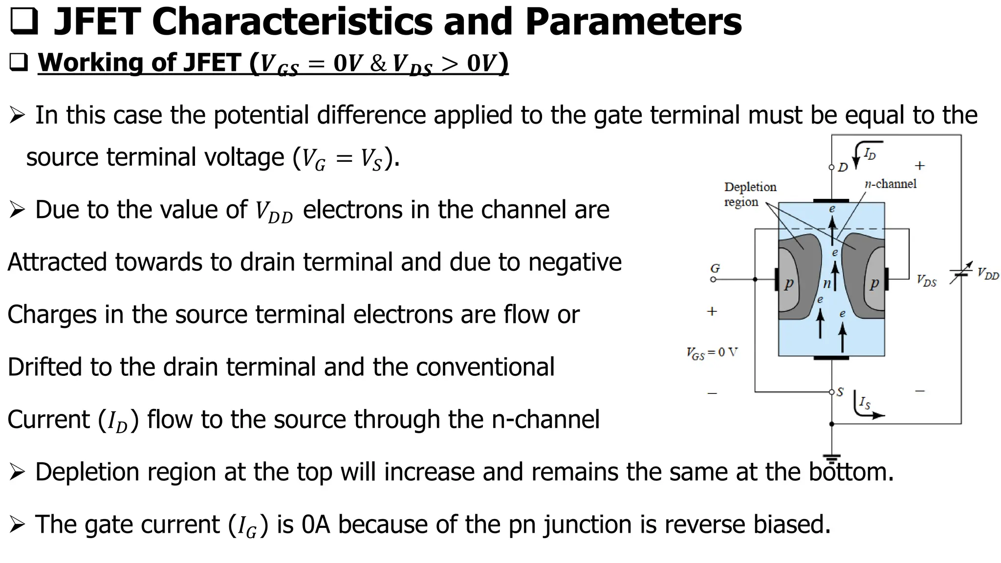
❑ JFET Characteristicsand Parameters
❑ Working of JFET (𝑽𝑮𝑺 = 𝟎𝑽 & 𝑽𝑫𝑺 > 𝟎𝑽)
➢ In this case the potential difference applied to the gate terminal must be equal to the
source terminal voltage (𝑉𝐺 = 𝑉𝑆).
➢ Due to the value of 𝑉𝐷𝐷 electrons in the channel are
Attracted towards to drain terminal and due to negative
Charges in the source terminal electrons are flow or
Drifted to the drain terminal and the conventional
Current (𝐼𝐷) flow to the source through the n-channel
➢ Depletion region at the top will increase and remains the same at the bottom.
➢ The gate current (𝐼𝐺) is 0A because of the pn junction is reverse biased.
10.
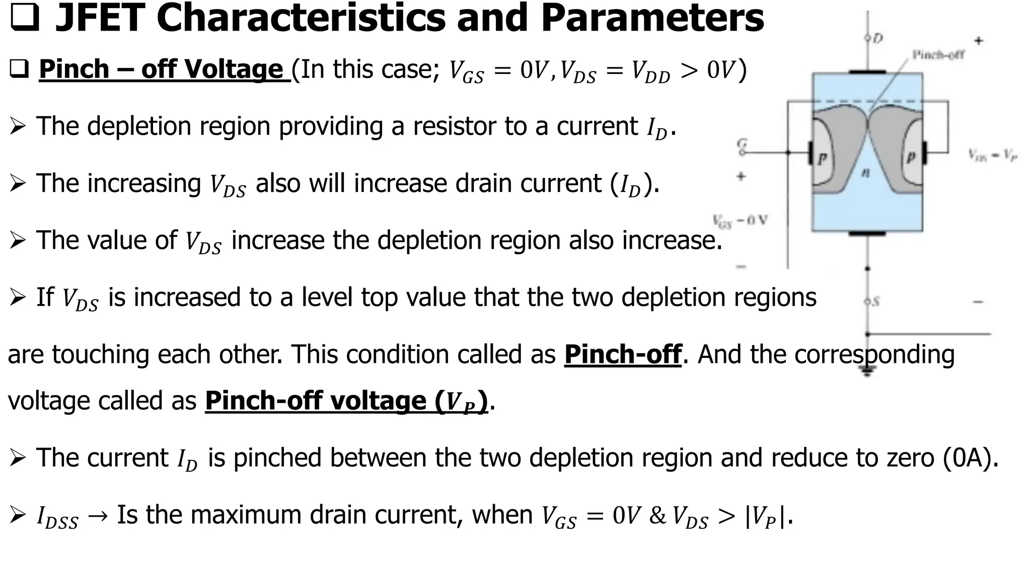
❑ Pinch –off Voltage (In this case; 𝑉𝐺𝑆 = 0𝑉, 𝑉𝐷𝑆 = 𝑉𝐷𝐷 > 0𝑉)
➢ The depletion region providing a resistor to a current 𝐼𝐷.
➢ The increasing 𝑉𝐷𝑆 also will increase drain current (𝐼𝐷).
➢ The value of 𝑉𝐷𝑆 increase the depletion region also increase.
➢ If 𝑉𝐷𝑆 is increased to a level top value that the two depletion regions
are touching each other. This condition called as Pinch-off. And the corresponding
voltage called as Pinch-off voltage (𝑽𝑷).
➢ The current 𝐼𝐷 is pinched between the two depletion region and reduce to zero (0A).
➢ 𝐼𝐷𝑆𝑆 → Is the maximum drain current, when 𝑉𝐺𝑆 = 0𝑉 & 𝑉𝐷𝑆 > |𝑉𝑃|.
❑ JFET Characteristics and Parameters
11.
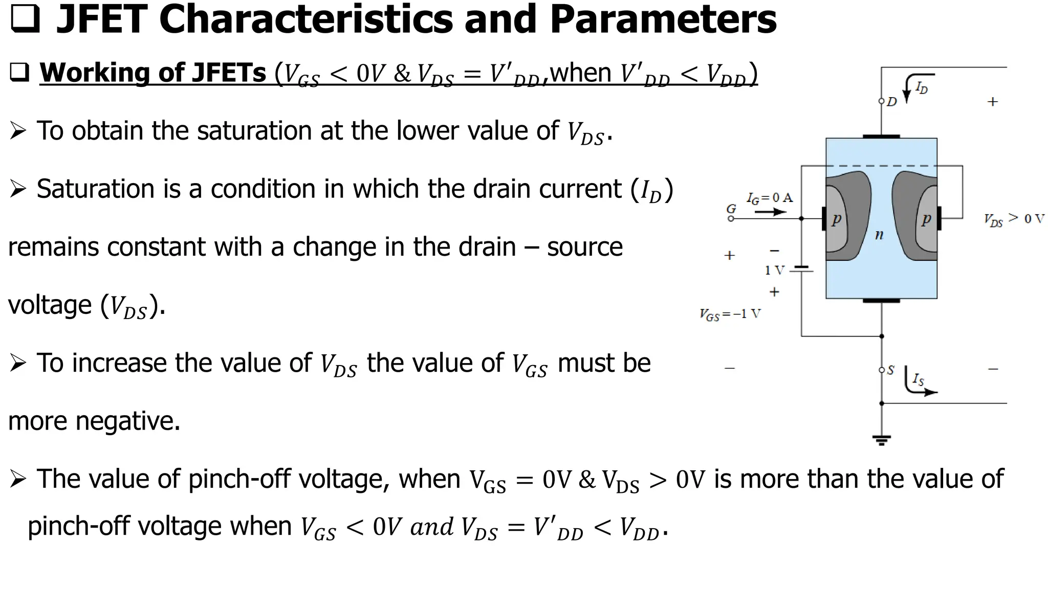
❑ JFET Characteristicsand Parameters
❑ Working of JFETs (𝑉𝐺𝑆 < 0𝑉 & 𝑉𝐷𝑆 = 𝑉′𝐷𝐷,when 𝑉′𝐷𝐷 < 𝑉𝐷𝐷)
➢ To obtain the saturation at the lower value of 𝑉𝐷𝑆.
➢ Saturation is a condition in which the drain current (𝐼𝐷)
remains constant with a change in the drain – source
voltage (𝑉𝐷𝑆).
➢ To increase the value of 𝑉𝐷𝑆 the value of 𝑉𝐺𝑆 must be
more negative.
➢ The value of pinch-off voltage, when VGS = 0V & VDS > 0V is more than the value of
pinch-off voltage when 𝑉𝐺𝑆 < 0𝑉 𝑎𝑛𝑑 𝑉𝐷𝑆 = 𝑉′𝐷𝐷 < 𝑉𝐷𝐷.
12.
❑ Introduction toFETs Biasing
➢ To find out the operating, we have two approaches,. These are
1. Mathematical Approach:- When the relationship is linear
2. Graphical Approach:- When the relationship is non-linear
➢ There are three basic types of biasing techniques. These are:-
1. Fixed-biasing configuration
2. Self-biasing configuration
3. Voltage-divider biasing configuration.
13.
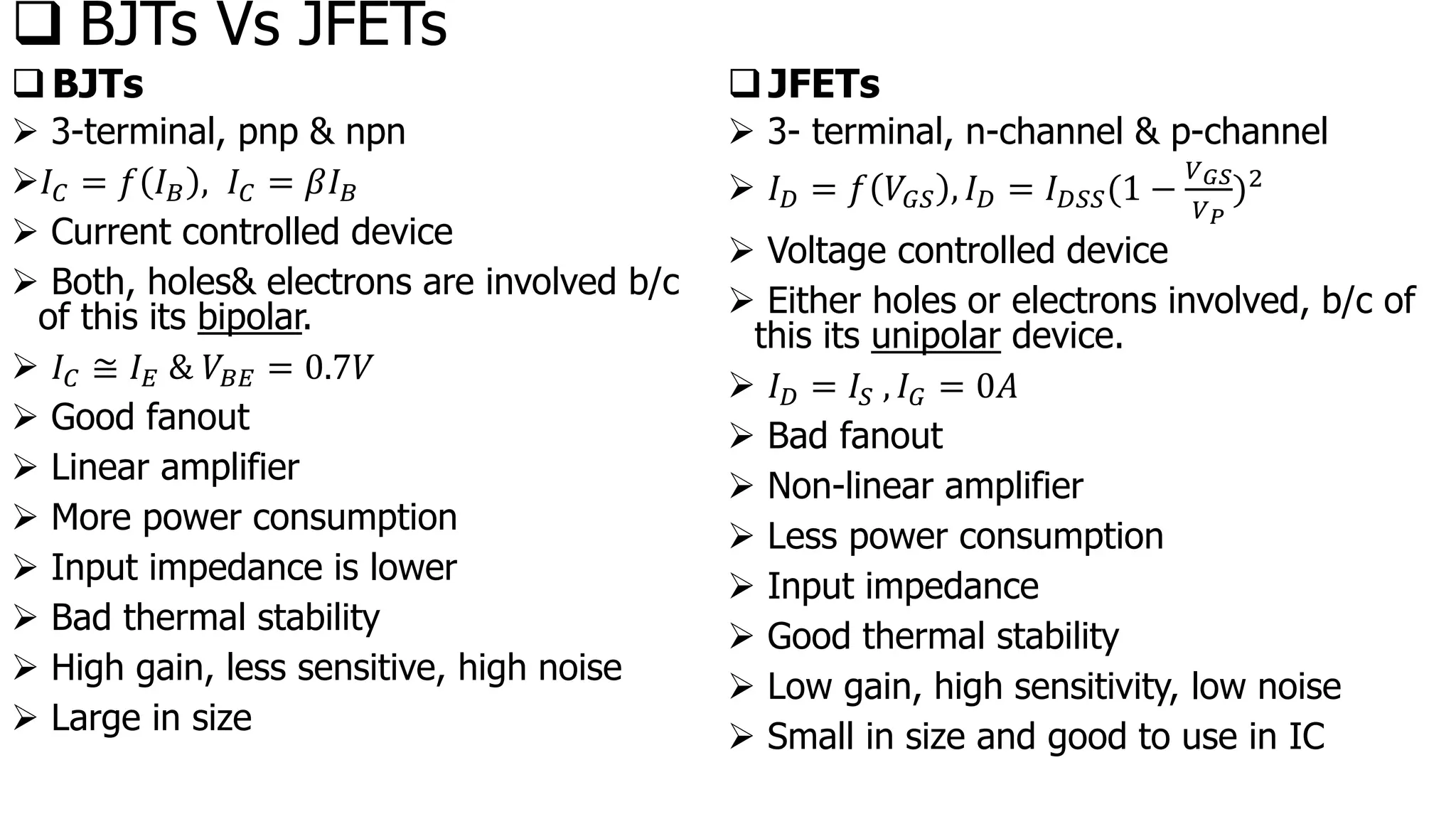
❑ BJTs VsJFETs
❑BJTs
➢ 3-terminal, pnp & npn
➢𝐼𝐶 = 𝑓 𝐼𝐵 , 𝐼𝐶 = 𝛽𝐼𝐵
➢ Current controlled device
➢ Both, holes& electrons are involved b/c
of this its bipolar.
➢ 𝐼𝐶 ≅ 𝐼𝐸 & 𝑉𝐵𝐸 = 0.7𝑉
➢ Good fanout
➢ Linear amplifier
➢ More power consumption
➢ Input impedance is lower
➢ Bad thermal stability
➢ High gain, less sensitive, high noise
➢ Large in size
❑JFETs
➢ 3- terminal, n-channel & p-channel
➢ 𝐼𝐷 = 𝑓 𝑉𝐺𝑆 , 𝐼𝐷 = 𝐼𝐷𝑆𝑆(1 −
𝑉𝐺𝑆
𝑉𝑃
)2
➢ Voltage controlled device
➢ Either holes or electrons involved, b/c of
this its unipolar device.
➢ 𝐼𝐷 = 𝐼𝑆 , 𝐼𝐺 = 0𝐴
➢ Bad fanout
➢ Non-linear amplifier
➢ Less power consumption
➢ Input impedance
➢ Good thermal stability
➢ Low gain, high sensitivity, low noise
➢ Small in size and good to use in IC
14.
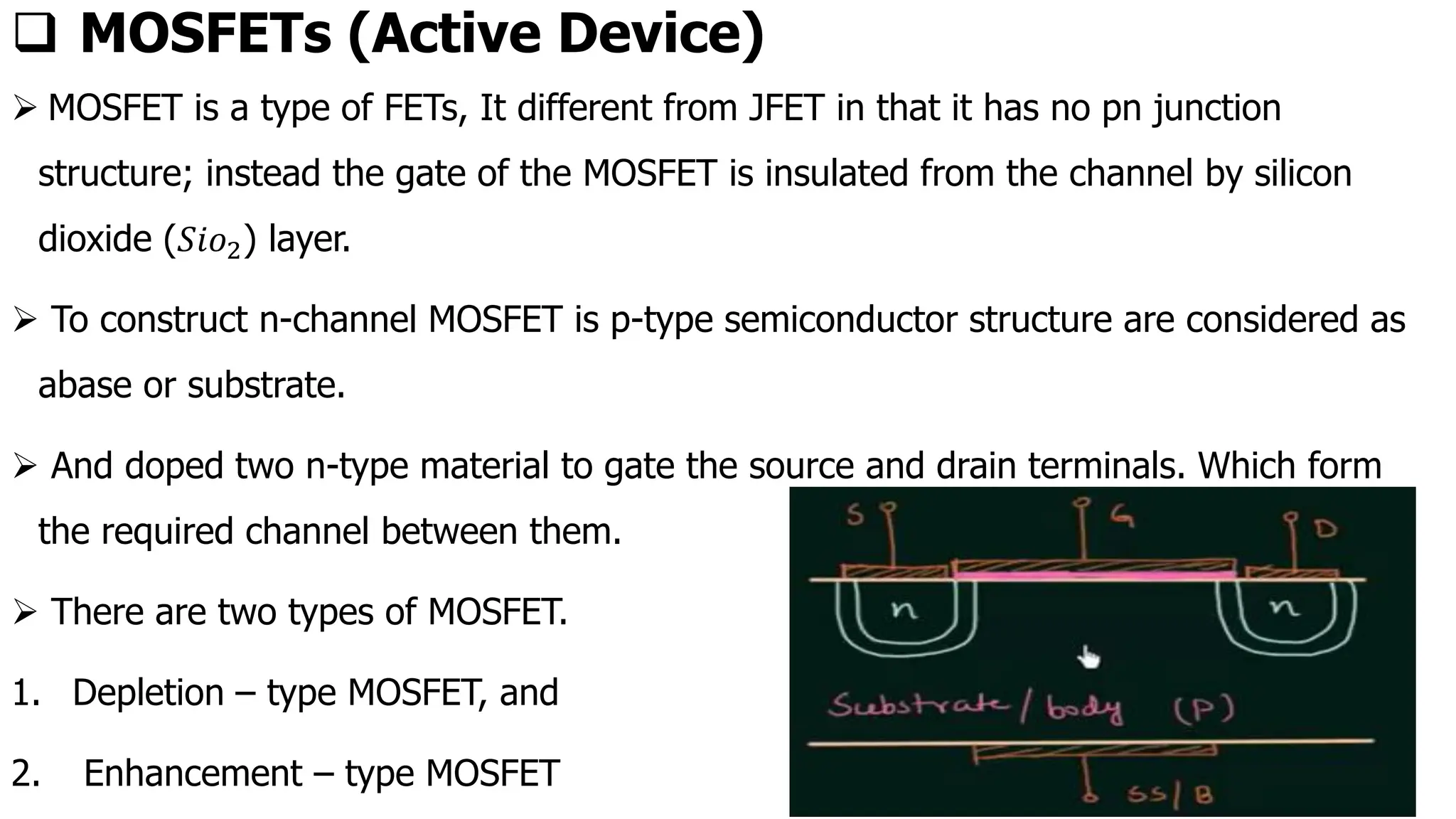
❑ MOSFETs (ActiveDevice)
➢ MOSFET is a type of FETs, It different from JFET in that it has no pn junction
structure; instead the gate of the MOSFET is insulated from the channel by silicon
dioxide (𝑆𝑖𝑜2) layer.
➢ To construct n-channel MOSFET is p-type semiconductor structure are considered as
abase or substrate.
➢ And doped two n-type material to gate the source and drain terminals. Which form
the required channel between them.
➢ There are two types of MOSFET.
1. Depletion – type MOSFET, and
2. Enhancement – type MOSFET
15.
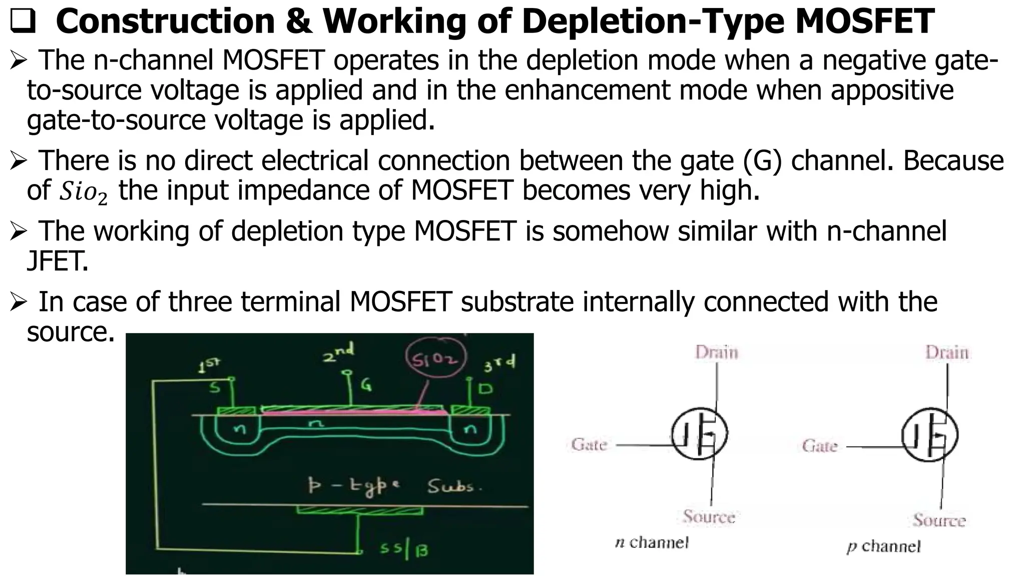
❑ Construction &Working of Depletion-Type MOSFET
➢ The n-channel MOSFET operates in the depletion mode when a negative gate-
to-source voltage is applied and in the enhancement mode when appositive
gate-to-source voltage is applied.
➢ There is no direct electrical connection between the gate (G) channel. Because
of 𝑆𝑖𝑜2 the input impedance of MOSFET becomes very high.
➢ The working of depletion type MOSFET is somehow similar with n-channel
JFET.
➢ In case of three terminal MOSFET substrate internally connected with the
source.
16.
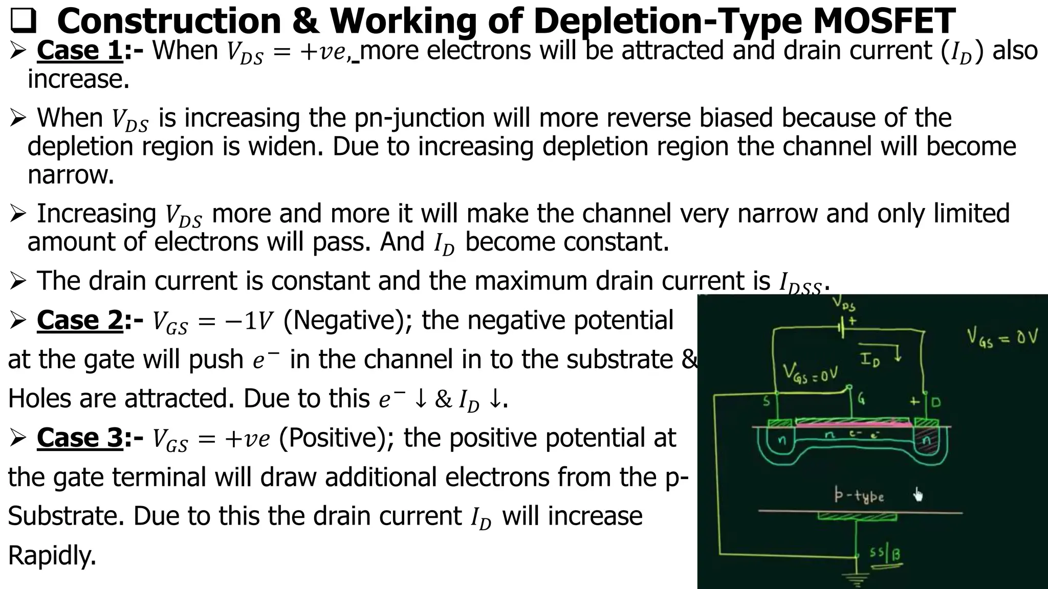
❑ Construction &Working of Depletion-Type MOSFET
➢ Case 1:- When 𝑉𝐷𝑆 = +𝑣𝑒, more electrons will be attracted and drain current (𝐼𝐷) also
increase.
➢ When 𝑉𝐷𝑆 is increasing the pn-junction will more reverse biased because of the
depletion region is widen. Due to increasing depletion region the channel will become
narrow.
➢ Increasing 𝑉𝐷𝑆 more and more it will make the channel very narrow and only limited
amount of electrons will pass. And 𝐼𝐷 become constant.
➢ The drain current is constant and the maximum drain current is 𝐼𝐷𝑆𝑆.
➢ Case 2:- 𝑉𝐺𝑆 = −1𝑉 (Negative); the negative potential
at the gate will push 𝑒− in the channel in to the substrate &
Holes are attracted. Due to this 𝑒− ↓ & 𝐼𝐷 ↓.
➢ Case 3:- 𝑉𝐺𝑆 = +𝑣𝑒 (Positive); the positive potential at
the gate terminal will draw additional electrons from the p-
Substrate. Due to this the drain current 𝐼𝐷 will increase
Rapidly.
17.
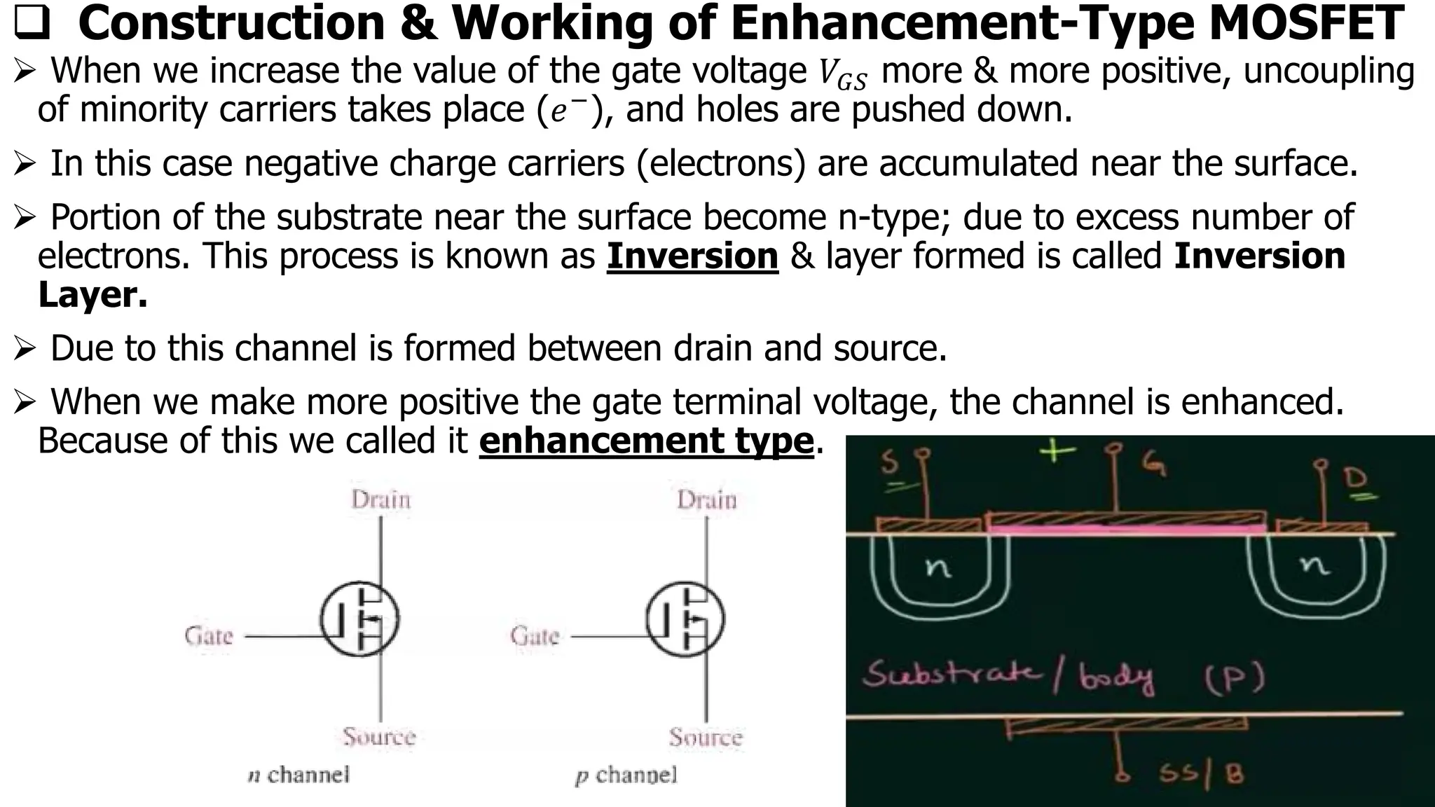
❑ Construction &Working of Enhancement-Type MOSFET
➢ When we increase the value of the gate voltage 𝑉𝐺𝑆 more & more positive, uncoupling
of minority carriers takes place (𝑒−), and holes are pushed down.
➢ In this case negative charge carriers (electrons) are accumulated near the surface.
➢ Portion of the substrate near the surface become n-type; due to excess number of
electrons. This process is known as Inversion & layer formed is called Inversion
Layer.
➢ Due to this channel is formed between drain and source.
➢ When we make more positive the gate terminal voltage, the channel is enhanced.
Because of this we called it enhancement type.
18.
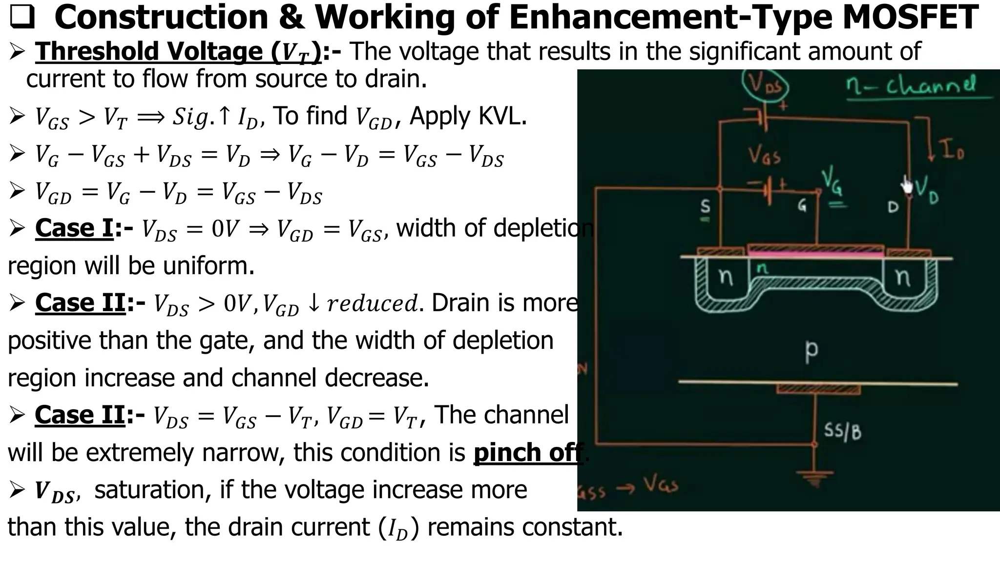
➢ Threshold Voltage(𝑽𝑻):- The voltage that results in the significant amount of
current to flow from source to drain.
➢ 𝑉𝐺𝑆 > 𝑉𝑇 ⟹ 𝑆𝑖𝑔. ↑ 𝐼𝐷, To find 𝑉𝐺𝐷, Apply KVL.
➢ 𝑉𝐺 − 𝑉𝐺𝑆 + 𝑉𝐷𝑆 = 𝑉𝐷 ⇒ 𝑉𝐺 − 𝑉𝐷 = 𝑉𝐺𝑆 − 𝑉𝐷𝑆
➢ 𝑉𝐺𝐷 = 𝑉𝐺 − 𝑉𝐷 = 𝑉𝐺𝑆 − 𝑉𝐷𝑆
➢ Case I:- 𝑉𝐷𝑆 = 0𝑉 ⇒ 𝑉𝐺𝐷 = 𝑉𝐺𝑆, width of depletion
region will be uniform.
➢ Case II:- 𝑉𝐷𝑆 > 0𝑉, 𝑉𝐺𝐷 ↓ 𝑟𝑒𝑑𝑢𝑐𝑒𝑑. Drain is more
positive than the gate, and the width of depletion
region increase and channel decrease.
➢ Case II:- 𝑉𝐷𝑆 = 𝑉𝐺𝑆 − 𝑉𝑇, 𝑉𝐺𝐷 = 𝑉𝑇, The channel
will be extremely narrow, this condition is pinch off.
➢ 𝑽𝑫𝑺, saturation, if the voltage increase more
than this value, the drain current (𝐼𝐷) remains constant.
❑ Construction & Working of Enhancement-Type MOSFET
19.
❑ Reading Assignment
➢Drain & Transfer Characteristics of JFET & MOSFET
❑ Assignment (Sub. Date may 27/2024)
1. In case of n-channel JFET the value of pinch-off voltage, when VGS = 0V & VDS > 0V is more
than the value of pinch-off voltage when 𝑉𝐺𝑆 < 0𝑉 𝑎𝑛𝑑 𝑉𝐷𝑆 = 𝑉′𝐷𝐷 < 𝑉𝐷𝐷. Why? Explain in
detail with net sketch.
2. In MOSFET, there is no electrical connectivity between the gate (G) terminal and the other
two source & drain terminals. But when we apply a DC external voltage source through the
gate terminal, the operational condition of a device will change. This means that when we
apply a positive voltage to the gate terminal for n-channel DMOSFET & EMOSFET, the
number of electrons will rapidly increase and the channel will be enhanced, respectively.
Also, the signal to be amplified is introduced through the gate terminal and taken from the
drain terminal. Explain how its happening.