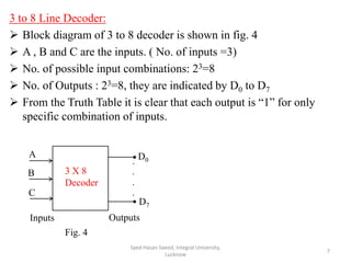
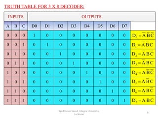
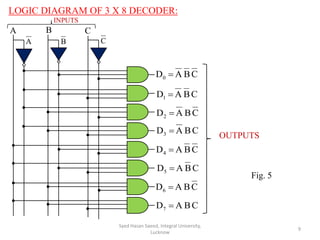
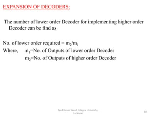
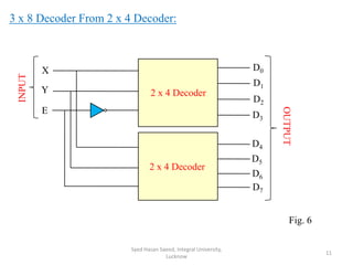
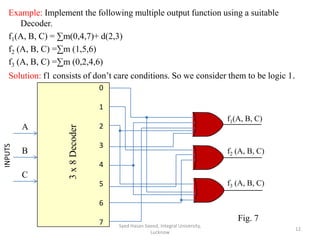
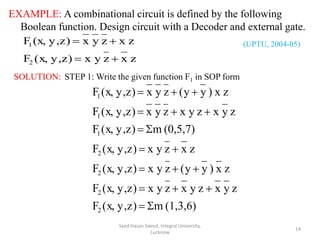
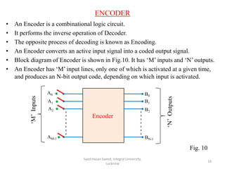
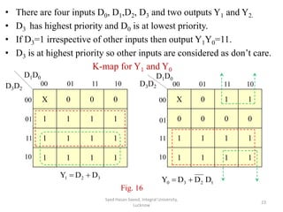
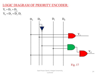
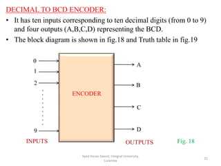
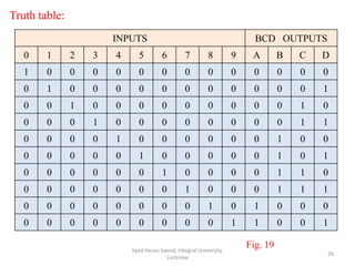
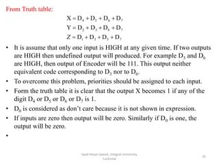
SYED HASAN SAEED
hasansaeedcontrol@gmail.com
https://shasansaeed.yolasite.com
1
Syed Hasan Saeed, Integral University,
Lucknow
DECODER
&
ENCODER
Syed Hasan Saeed, Integral University,
Lucknow
2
DECODER
• A decoder is a combinational circuit.
• A decoder accepts a set of inputs that represents a binary
number and activates only that output corresponding to the
input number. All other outputs remain inactive.
• Fig. 1 shows the block diagram of decoder with ‘N’ inputs and
‘M’ outputs.
• There are 2N possible input combinations, for each of these
input combination only one output will be HIGH (active) all
other outputs are LOW
• Some decoder have one or more ENABLE (E) inputs that are
used to control the operation of decoder.
Syed Hasan Saeed, Integral University,
Lucknow
3
BLOCK DIAGRAM OF DECODER
Syed Hasan Saeed, Integral University,
Lucknow
4
DECODER
A0
A1
A2
AN-1
.
.
.
.
N- Inputs M- Outputs
.
.
.
.
B0
B1
B2
BM-1
Only one output is High for
each input
Fig. 1
2 to 4 Line Decoder:
 Block diagram of 2 to 4 decoder is shown in fig. 2
 A and B are the inputs. ( No. of inputs =2)
 No. of possible input combinations: 22=4
 No. of Outputs : 22=4, they are indicated by D0, D1, D2 and D3
 From the Truth Table it is clear that each output is “1” for only
specific combination of inputs.
Syed Hasan Saeed, Integral University,
Lucknow
5
A
B
D0
D1
D2
D3
2 X 4
Decoder
INPUTS OUTPUTS
A B D0 D1 D2 D3
0 0 1 0 0 0
0 1 0 1 0 0
1 0 0 0 1 0
1 1 0 0 0 1
Fig. 2
TRUTH TABLE
Inputs Outputs
BOOLEAN EXPRESSION:
Syed Hasan Saeed, Integral University,
Lucknow
6
ABDBAD
BADBAD
32
10


From Truth Table
LOGIC DIAGRAM:
A
A
B
B
BAD0 
BAD1 
BAD2 
BAD3 
Fig. 3
3 to 8 Line Decoder:
 Block diagram of 3 to 8 decoder is shown in fig. 4
 A , B and C are the inputs. ( No. of inputs =3)
 No. of possible input combinations: 23=8
 No. of Outputs : 23=8, they are indicated by D0 to D7
 From the Truth Table it is clear that each output is “1” for only
specific combination of inputs.
Syed Hasan Saeed, Integral University,
Lucknow
7
A
B
D0
D7
3 X 8
Decoder
C
.
.
.
.
Fig. 4
Inputs Outputs
TRUTH TABLE FOR 3 X 8 DECODER:
Syed Hasan Saeed, Integral University,
Lucknow
8
INPUTS OUTPUTS
A B C D0 D1 D2 D3 D4 D5 D6 D7
0 0 0 1 0 0 0 0 0 0 0
0 0 1 0 1 0 0 0 0 0 0
0 1 0 0 0 1 0 0 0 0 0
0 1 1 0 0 0 1 0 0 0 0
1 0 0 0 0 0 0 1 0 0 0
1 0 1 0 0 0 0 0 1 0 0
1 1 0 0 0 0 0 0 0 1 0
1 1 1 0 0 0 0 0 0 0 1
CBAD0 
CBAD1 
CBAD2 
CBAD3 
CBAD4 
CBAD5 
CBAD6 
CBAD7 
LOGIC DIAGRAM OF 3 X 8 DECODER:
Syed Hasan Saeed, Integral University,
Lucknow
9
CBAD0 
CBAD1 
CBAD2 
CBAD3 
CBAD4 
CBAD5 
CBAD6 
CBAD7 
A B C
A B C
OUTPUTS
INPUTS
Fig. 5
EXPANSION OF DECODERS:
The number of lower order Decoder for implementing higher order
Decoder can be find as
No. of lower order required = m2/m1
Where, m1=No. of Outputs of lower order Decoder
m2=No. of Outputs of higher order Decoder
Syed Hasan Saeed, Integral University,
Lucknow
10
3 x 8 Decoder From 2 x 4 Decoder:
Syed Hasan Saeed, Integral University,
Lucknow
11
2 x 4 Decoder
2 x 4 Decoder
X
Y
E
D0
D1
D2
D3
D4
D5
D6
D7
OUTPUT
INPUT
Fig. 6
Example: Implement the following multiple output function using a suitable
Decoder.
f1(A, B, C) = ∑m(0,4,7)+ d(2,3)
f2 (A, B, C) =∑m (1,5,6)
f3 (A, B, C) =∑m (0,2,4,6)
Solution: f1 consists of don’t care conditions. So we consider them to be logic 1.
Syed Hasan Saeed, Integral University,
Lucknow
12
0
1
2
3
4
5
6
7
f1(A, B, C)
f2 (A, B, C)
f3 (A, B, C)
3x8Decoder
A
B
C
INPUTS
Fig. 7
EXAMPLE: Implement the following Boolean function using suitable Decoder.
f1 (x,y,z)=∑m(1,5,7)
f2 (x,y,z)=∑m(0,3)
f3 (x,y,z)=∑m(2,4,5)
Solution:
Syed Hasan Saeed, Integral University,
Lucknow
13
X
Y
Z
E
3X8Decoder
0
1
2
3
4
5
6
7
INPUTS
f1 (x,y,z)
f2 (x,y,z)
f3 (x,y,z)
Fig. 8
EXAMPLE: A combinational circuit is defined by the following
Boolean function. Design circuit with a Decoder and external gate.
Syed Hasan Saeed, Integral University,
Lucknow
14
zxzyxz)y,x,(F
zxzyxz)y,(x,F
2
1


SOLUTION: STEP 1: Write the given function F1 in SOP form
(1,3,6)mz)y,x,(F
zyxzyxzyxz)y,x,(F
zx)yy(zyxz)y,x,(F
zxzyxz)y,x,(F
(0,5,7)mz)y,x,(F
zyxzyxzyxz)y,x,(F
zx)yy(zyxz)y,x,(F
2
2
2
2
1
1
1







(UPTU, 2004-05)
Boolean Function using Decoder:
Syed Hasan Saeed, Integral University,
Lucknow
15
0
1
2
3
4
5
6
7
F1
F2
3 x 8
Decoder
X
Y
Z
Fig. 9
ENCODER
• An Encoder is a combinational logic circuit.
• It performs the inverse operation of Decoder.
• The opposite process of decoding is known as Encoding.
• An Encoder converts an active input signal into a coded output signal.
• Block diagram of Encoder is shown in Fig.10. It has ‘M’ inputs and ‘N’ outputs.
• An Encoder has ‘M’ input lines, only one of which is activated at a given time,
and produces an N-bit output code, depending on which input is activated.
Syed Hasan Saeed, Integral University,
Lucknow
16
-------
-------
‘M’Inputs
‘N’Outputs
Encoder
A0
A1
A2
AM-1
B0
B1
B2
BN-1
Fig. 10
• Encoders are used to translate the rotary or linear motion into a digital
signal.
• The difference between Decoder and Encoder is that Decoder has Binary
Code as an input while Encoder has Binary Code as an output.
• Encoder is an Electronics device that converts the analog signal to digital
signal such as BCD Code.
• Types of Encoders
i. Priority Encoder
ii. Decimal to BCD Encoder
iii. Octal to Binary Encoder
iv. Hexadecimal to Binary Encoder
Syed Hasan Saeed, Integral University,
Lucknow
17
ENCODER
Syed Hasan Saeed, Integral University,
Lucknow
18
Encoder
4 x 2
A0
A1
A2
Fig. 11
Decoder
2 x 4A3
M=4
M=22
M=2N
‘M’ is the input and
‘N’ is the output
B0
B1
B2
B3
ENCODER
Syed Hasan Saeed, Integral University,
Lucknow
19
Encoder
4 x 2
A0
A1
A2
Fig. 12
Decoder
2 x 4A3
M=4
M=22
M=2N
‘M’ is the input and
‘N’ is the output
00
01
10
11
ENCODER
Syed Hasan Saeed, Integral University,
Lucknow
20
Encoder
4 x 2
A0
A1
A2
Fig. 13
Decoder
2 x 4A3
M=4
M=22
M=2N
‘M’ is the input and
‘N’ is the output
00
01
10
11
1
0
ENCODER
Syed Hasan Saeed, Integral University,
Lucknow
21
Encoder
4 x 2
A0
A1
A2
Fig. 14
Decoder
2 x 4A3
M=4
M=22
M=2N
‘M’ is the input and
‘N’ is the output
00
01
10
11
1
0 10
PRIORITY ENCODER:
• As the name indicates, the priority is given to inputs line.
• If two or more input lines are high at the same time i.e 1 at the same time,
then the input line with high priority shall be considered.
• Block diagram and Truth table of Priority Encoder are shown in fig.15
Syed Hasan Saeed, Integral University,
Lucknow
22
D3
D2
D1
D0
Y1
Y0
Highest Priority
Input
Lowest Priority
Input
Output
Priority
Encoder
INPUTS OUTPUTS V
0 0 0 0 x x 0
0 0 0 1 0 0 1
0 0 1 x 0 1 1
0 1 x x 1 0 1
1 x x x 1 1 1
D3 D2 D1 D0 Y1 Y0
TRUTH TABLE:
Fig.15Block Diagram of Priority
Encoder
• There are four inputs D0, D1,D2, D3 and two outputs Y1 and Y2.
• D3 has highest priority and D0 is at lowest priority.
• If D3=1 irrespective of other inputs then output Y1Y0=11.
• D3 is at highest priority so other inputs are considered as don’t care.
Syed Hasan Saeed, Integral University,
Lucknow
23
X 0 0 0
1 1 1 1
1 1 1 1
1 1 1 1
X 0 1 1
0 0 0 0
1 1 1 1
1 1 1 1
D3D2
D3D2
D1D0 D1D0
00 01 11 10 00 01 11 10
00
01
11
10 10
11
01
00
1230 DDDY 321 DDY 
K-map for Y1 and Y0
Fig. 16
LOGIC DIAGRAM OF PRIORITY ENCODER:
Syed Hasan Saeed, Integral University,
Lucknow
24
321 DDY 
1230 DDDY 
D3 D2 D1 D0
Y1
Y0
Fig. 17
DECIMAL TO BCD ENCODER:
• It has ten inputs corresponding to ten decimal digits (from 0 to 9)
and four outputs (A,B,C,D) representing the BCD.
• The block diagram is shown in fig.18 and Truth table in fig.19
Syed Hasan Saeed, Integral University,
Lucknow
25
---------
ENCODER
0
1
2
9
A
B
C
D
INPUTS OUTPUTS Fig. 18
Truth table:
Syed Hasan Saeed, Integral University,
Lucknow
26
INPUTS BCD OUTPUTS
0 1 2 3 4 5 6 7 8 9 A B C D
1 0 0 0 0 0 0 0 0 0 0 0 0 0
0 1 0 0 0 0 0 0 0 0 0 0 0 1
0 0 1 0 0 0 0 0 0 0 0 0 1 0
0 0 0 1 0 0 0 0 0 0 0 0 1 1
0 0 0 0 1 0 0 0 0 0 0 1 0 0
0 0 0 0 0 1 0 0 0 0 0 1 0 1
0 0 0 0 0 0 1 0 0 0 0 1 1 0
0 0 0 0 0 0 0 1 0 0 0 1 1 1
0 0 0 0 0 0 0 0 1 0 1 0 0 0
0 0 0 0 0 0 0 0 0 1 1 0 0 1
Fig. 19
• From Truth Table it is clear that the output A is HIGH when input is
8 OR 9 is HIGH
Therefore A=8+9
• The output B is HIGH when 4 OR 5 OR 6 OR 7 is HIGH
Therefore B=4+5+6+7
• The output C is HIGH when 2 OR 3 OR 6 OR 7 is HIGH
Therefore C=2+3+6+7
• Similarly D=1+3+5+7+9
Logic Diagram is shown in fig.20
Syed Hasan Saeed, Integral University,
Lucknow
27
DECIMAL TO BCD ENCODER
Syed Hasan Saeed, Integral University,
Lucknow
28
0
1
2
3
4
5
6
7
8
9
A B C D
+5V
Fig. 20
OCTAL TO BINARY ENCODER:
• Block Diagram of Octal to Binary Encoder is shown in Fig. 21
• It has eight inputs and three outputs.
• Only one input has one value at any given time.
• Each input corresponds to each octal digit and output generates
corresponding Binary Code.
Syed Hasan Saeed, Integral University,
Lucknow
29
D0
D1
D2
D3
D4
D5
D6
D7
X
Y
Z
INPUT OUTPUT
ENCODER
Fig. 21
TRUTH TABLE:
Syed Hasan Saeed, Integral University,
Lucknow
30
INPUT OUTPUT
D0 D1 D2 D3 D4 D5 D6 D7 X Y Z
1 0 0 0 0 0 0 0 0 0 0
0 1 0 0 0 0 0 0 0 0 1
0 0 1 0 0 0 0 0 0 1 0
0 0 0 1 0 0 0 0 0 1 1
0 0 0 0 1 0 0 0 1 0 0
0 0 0 0 0 1 0 0 1 0 1
0 0 0 0 0 0 1 0 1 1 0
0 0 0 0 0 0 0 1 1 1 1
Fig.22
From Truth table:
• It is assume that only one input is HIGH at any given time. If two outputs
are HIGH then undefined output will produced. For example D3 and D6
are HIGH, then output of Encoder will be 111. This output neither
equivalent code corresponding to D3 nor to D6.
• To overcome this problem, priorities should be assigned to each input.
• Form the truth table it is clear that the output X becomes 1 if any of the
digit D4 or D5 or D6 or D7 is 1.
• D0 is considered as don’t care because it is not shown in expression.
• If inputs are zero then output will be zero. Similarly if D0 is one, the
output will be zero.
•
Syed Hasan Saeed, Integral University,
Lucknow
31
7531
7632
7654
DDDD
DDDDY
DDDDX



Z
Syed Hasan Saeed, Integral University,
Lucknow
32
7531
7632
7654
DDDD
DDDDY
DDDDX



Z
D0 D2 D3 D4 D5 D6 D7
D1
7654 DDDDX 
7632 DDDDY 
7531 DDDD Z
Fig. 23
LOGIC DIAGRAM:
THANK YOU
Syed Hasan Saeed, Integral University,
Lucknow
33

Encoder & Decoder

  • 1.
  • 2.
    DECODER & ENCODER Syed Hasan Saeed,Integral University, Lucknow 2
  • 3.
    DECODER • A decoderis a combinational circuit. • A decoder accepts a set of inputs that represents a binary number and activates only that output corresponding to the input number. All other outputs remain inactive. • Fig. 1 shows the block diagram of decoder with ‘N’ inputs and ‘M’ outputs. • There are 2N possible input combinations, for each of these input combination only one output will be HIGH (active) all other outputs are LOW • Some decoder have one or more ENABLE (E) inputs that are used to control the operation of decoder. Syed Hasan Saeed, Integral University, Lucknow 3
  • 4.
    BLOCK DIAGRAM OFDECODER Syed Hasan Saeed, Integral University, Lucknow 4 DECODER A0 A1 A2 AN-1 . . . . N- Inputs M- Outputs . . . . B0 B1 B2 BM-1 Only one output is High for each input Fig. 1
  • 5.
    2 to 4Line Decoder:  Block diagram of 2 to 4 decoder is shown in fig. 2  A and B are the inputs. ( No. of inputs =2)  No. of possible input combinations: 22=4  No. of Outputs : 22=4, they are indicated by D0, D1, D2 and D3  From the Truth Table it is clear that each output is “1” for only specific combination of inputs. Syed Hasan Saeed, Integral University, Lucknow 5 A B D0 D1 D2 D3 2 X 4 Decoder INPUTS OUTPUTS A B D0 D1 D2 D3 0 0 1 0 0 0 0 1 0 1 0 0 1 0 0 0 1 0 1 1 0 0 0 1 Fig. 2 TRUTH TABLE Inputs Outputs
  • 6.
    BOOLEAN EXPRESSION: Syed HasanSaeed, Integral University, Lucknow 6 ABDBAD BADBAD 32 10   From Truth Table LOGIC DIAGRAM: A A B B BAD0  BAD1  BAD2  BAD3  Fig. 3
  • 7.
    3 to 8Line Decoder:  Block diagram of 3 to 8 decoder is shown in fig. 4  A , B and C are the inputs. ( No. of inputs =3)  No. of possible input combinations: 23=8  No. of Outputs : 23=8, they are indicated by D0 to D7  From the Truth Table it is clear that each output is “1” for only specific combination of inputs. Syed Hasan Saeed, Integral University, Lucknow 7 A B D0 D7 3 X 8 Decoder C . . . . Fig. 4 Inputs Outputs
  • 8.
    TRUTH TABLE FOR3 X 8 DECODER: Syed Hasan Saeed, Integral University, Lucknow 8 INPUTS OUTPUTS A B C D0 D1 D2 D3 D4 D5 D6 D7 0 0 0 1 0 0 0 0 0 0 0 0 0 1 0 1 0 0 0 0 0 0 0 1 0 0 0 1 0 0 0 0 0 0 1 1 0 0 0 1 0 0 0 0 1 0 0 0 0 0 0 1 0 0 0 1 0 1 0 0 0 0 0 1 0 0 1 1 0 0 0 0 0 0 0 1 0 1 1 1 0 0 0 0 0 0 0 1 CBAD0  CBAD1  CBAD2  CBAD3  CBAD4  CBAD5  CBAD6  CBAD7 
  • 9.
    LOGIC DIAGRAM OF3 X 8 DECODER: Syed Hasan Saeed, Integral University, Lucknow 9 CBAD0  CBAD1  CBAD2  CBAD3  CBAD4  CBAD5  CBAD6  CBAD7  A B C A B C OUTPUTS INPUTS Fig. 5
  • 10.
    EXPANSION OF DECODERS: Thenumber of lower order Decoder for implementing higher order Decoder can be find as No. of lower order required = m2/m1 Where, m1=No. of Outputs of lower order Decoder m2=No. of Outputs of higher order Decoder Syed Hasan Saeed, Integral University, Lucknow 10
  • 11.
    3 x 8Decoder From 2 x 4 Decoder: Syed Hasan Saeed, Integral University, Lucknow 11 2 x 4 Decoder 2 x 4 Decoder X Y E D0 D1 D2 D3 D4 D5 D6 D7 OUTPUT INPUT Fig. 6
  • 12.
    Example: Implement thefollowing multiple output function using a suitable Decoder. f1(A, B, C) = ∑m(0,4,7)+ d(2,3) f2 (A, B, C) =∑m (1,5,6) f3 (A, B, C) =∑m (0,2,4,6) Solution: f1 consists of don’t care conditions. So we consider them to be logic 1. Syed Hasan Saeed, Integral University, Lucknow 12 0 1 2 3 4 5 6 7 f1(A, B, C) f2 (A, B, C) f3 (A, B, C) 3x8Decoder A B C INPUTS Fig. 7
  • 13.
    EXAMPLE: Implement thefollowing Boolean function using suitable Decoder. f1 (x,y,z)=∑m(1,5,7) f2 (x,y,z)=∑m(0,3) f3 (x,y,z)=∑m(2,4,5) Solution: Syed Hasan Saeed, Integral University, Lucknow 13 X Y Z E 3X8Decoder 0 1 2 3 4 5 6 7 INPUTS f1 (x,y,z) f2 (x,y,z) f3 (x,y,z) Fig. 8
  • 14.
    EXAMPLE: A combinationalcircuit is defined by the following Boolean function. Design circuit with a Decoder and external gate. Syed Hasan Saeed, Integral University, Lucknow 14 zxzyxz)y,x,(F zxzyxz)y,(x,F 2 1   SOLUTION: STEP 1: Write the given function F1 in SOP form (1,3,6)mz)y,x,(F zyxzyxzyxz)y,x,(F zx)yy(zyxz)y,x,(F zxzyxz)y,x,(F (0,5,7)mz)y,x,(F zyxzyxzyxz)y,x,(F zx)yy(zyxz)y,x,(F 2 2 2 2 1 1 1        (UPTU, 2004-05)
  • 15.
    Boolean Function usingDecoder: Syed Hasan Saeed, Integral University, Lucknow 15 0 1 2 3 4 5 6 7 F1 F2 3 x 8 Decoder X Y Z Fig. 9
  • 16.
    ENCODER • An Encoderis a combinational logic circuit. • It performs the inverse operation of Decoder. • The opposite process of decoding is known as Encoding. • An Encoder converts an active input signal into a coded output signal. • Block diagram of Encoder is shown in Fig.10. It has ‘M’ inputs and ‘N’ outputs. • An Encoder has ‘M’ input lines, only one of which is activated at a given time, and produces an N-bit output code, depending on which input is activated. Syed Hasan Saeed, Integral University, Lucknow 16 ------- ------- ‘M’Inputs ‘N’Outputs Encoder A0 A1 A2 AM-1 B0 B1 B2 BN-1 Fig. 10
  • 17.
    • Encoders areused to translate the rotary or linear motion into a digital signal. • The difference between Decoder and Encoder is that Decoder has Binary Code as an input while Encoder has Binary Code as an output. • Encoder is an Electronics device that converts the analog signal to digital signal such as BCD Code. • Types of Encoders i. Priority Encoder ii. Decimal to BCD Encoder iii. Octal to Binary Encoder iv. Hexadecimal to Binary Encoder Syed Hasan Saeed, Integral University, Lucknow 17
  • 18.
    ENCODER Syed Hasan Saeed,Integral University, Lucknow 18 Encoder 4 x 2 A0 A1 A2 Fig. 11 Decoder 2 x 4A3 M=4 M=22 M=2N ‘M’ is the input and ‘N’ is the output B0 B1 B2 B3
  • 19.
    ENCODER Syed Hasan Saeed,Integral University, Lucknow 19 Encoder 4 x 2 A0 A1 A2 Fig. 12 Decoder 2 x 4A3 M=4 M=22 M=2N ‘M’ is the input and ‘N’ is the output 00 01 10 11
  • 20.
    ENCODER Syed Hasan Saeed,Integral University, Lucknow 20 Encoder 4 x 2 A0 A1 A2 Fig. 13 Decoder 2 x 4A3 M=4 M=22 M=2N ‘M’ is the input and ‘N’ is the output 00 01 10 11 1 0
  • 21.
    ENCODER Syed Hasan Saeed,Integral University, Lucknow 21 Encoder 4 x 2 A0 A1 A2 Fig. 14 Decoder 2 x 4A3 M=4 M=22 M=2N ‘M’ is the input and ‘N’ is the output 00 01 10 11 1 0 10
  • 22.
    PRIORITY ENCODER: • Asthe name indicates, the priority is given to inputs line. • If two or more input lines are high at the same time i.e 1 at the same time, then the input line with high priority shall be considered. • Block diagram and Truth table of Priority Encoder are shown in fig.15 Syed Hasan Saeed, Integral University, Lucknow 22 D3 D2 D1 D0 Y1 Y0 Highest Priority Input Lowest Priority Input Output Priority Encoder INPUTS OUTPUTS V 0 0 0 0 x x 0 0 0 0 1 0 0 1 0 0 1 x 0 1 1 0 1 x x 1 0 1 1 x x x 1 1 1 D3 D2 D1 D0 Y1 Y0 TRUTH TABLE: Fig.15Block Diagram of Priority Encoder
  • 23.
    • There arefour inputs D0, D1,D2, D3 and two outputs Y1 and Y2. • D3 has highest priority and D0 is at lowest priority. • If D3=1 irrespective of other inputs then output Y1Y0=11. • D3 is at highest priority so other inputs are considered as don’t care. Syed Hasan Saeed, Integral University, Lucknow 23 X 0 0 0 1 1 1 1 1 1 1 1 1 1 1 1 X 0 1 1 0 0 0 0 1 1 1 1 1 1 1 1 D3D2 D3D2 D1D0 D1D0 00 01 11 10 00 01 11 10 00 01 11 10 10 11 01 00 1230 DDDY 321 DDY  K-map for Y1 and Y0 Fig. 16
  • 24.
    LOGIC DIAGRAM OFPRIORITY ENCODER: Syed Hasan Saeed, Integral University, Lucknow 24 321 DDY  1230 DDDY  D3 D2 D1 D0 Y1 Y0 Fig. 17
  • 25.
    DECIMAL TO BCDENCODER: • It has ten inputs corresponding to ten decimal digits (from 0 to 9) and four outputs (A,B,C,D) representing the BCD. • The block diagram is shown in fig.18 and Truth table in fig.19 Syed Hasan Saeed, Integral University, Lucknow 25 --------- ENCODER 0 1 2 9 A B C D INPUTS OUTPUTS Fig. 18
  • 26.
    Truth table: Syed HasanSaeed, Integral University, Lucknow 26 INPUTS BCD OUTPUTS 0 1 2 3 4 5 6 7 8 9 A B C D 1 0 0 0 0 0 0 0 0 0 0 0 0 0 0 1 0 0 0 0 0 0 0 0 0 0 0 1 0 0 1 0 0 0 0 0 0 0 0 0 1 0 0 0 0 1 0 0 0 0 0 0 0 0 1 1 0 0 0 0 1 0 0 0 0 0 0 1 0 0 0 0 0 0 0 1 0 0 0 0 0 1 0 1 0 0 0 0 0 0 1 0 0 0 0 1 1 0 0 0 0 0 0 0 0 1 0 0 0 1 1 1 0 0 0 0 0 0 0 0 1 0 1 0 0 0 0 0 0 0 0 0 0 0 0 1 1 0 0 1 Fig. 19
  • 27.
    • From TruthTable it is clear that the output A is HIGH when input is 8 OR 9 is HIGH Therefore A=8+9 • The output B is HIGH when 4 OR 5 OR 6 OR 7 is HIGH Therefore B=4+5+6+7 • The output C is HIGH when 2 OR 3 OR 6 OR 7 is HIGH Therefore C=2+3+6+7 • Similarly D=1+3+5+7+9 Logic Diagram is shown in fig.20 Syed Hasan Saeed, Integral University, Lucknow 27
  • 28.
    DECIMAL TO BCDENCODER Syed Hasan Saeed, Integral University, Lucknow 28 0 1 2 3 4 5 6 7 8 9 A B C D +5V Fig. 20
  • 29.
    OCTAL TO BINARYENCODER: • Block Diagram of Octal to Binary Encoder is shown in Fig. 21 • It has eight inputs and three outputs. • Only one input has one value at any given time. • Each input corresponds to each octal digit and output generates corresponding Binary Code. Syed Hasan Saeed, Integral University, Lucknow 29 D0 D1 D2 D3 D4 D5 D6 D7 X Y Z INPUT OUTPUT ENCODER Fig. 21
  • 30.
    TRUTH TABLE: Syed HasanSaeed, Integral University, Lucknow 30 INPUT OUTPUT D0 D1 D2 D3 D4 D5 D6 D7 X Y Z 1 0 0 0 0 0 0 0 0 0 0 0 1 0 0 0 0 0 0 0 0 1 0 0 1 0 0 0 0 0 0 1 0 0 0 0 1 0 0 0 0 0 1 1 0 0 0 0 1 0 0 0 1 0 0 0 0 0 0 0 1 0 0 1 0 1 0 0 0 0 0 0 1 0 1 1 0 0 0 0 0 0 0 0 1 1 1 1 Fig.22
  • 31.
    From Truth table: •It is assume that only one input is HIGH at any given time. If two outputs are HIGH then undefined output will produced. For example D3 and D6 are HIGH, then output of Encoder will be 111. This output neither equivalent code corresponding to D3 nor to D6. • To overcome this problem, priorities should be assigned to each input. • Form the truth table it is clear that the output X becomes 1 if any of the digit D4 or D5 or D6 or D7 is 1. • D0 is considered as don’t care because it is not shown in expression. • If inputs are zero then output will be zero. Similarly if D0 is one, the output will be zero. • Syed Hasan Saeed, Integral University, Lucknow 31 7531 7632 7654 DDDD DDDDY DDDDX    Z
  • 32.
    Syed Hasan Saeed,Integral University, Lucknow 32 7531 7632 7654 DDDD DDDDY DDDDX    Z D0 D2 D3 D4 D5 D6 D7 D1 7654 DDDDX  7632 DDDDY  7531 DDDD Z Fig. 23 LOGIC DIAGRAM:
  • 33.
    THANK YOU Syed HasanSaeed, Integral University, Lucknow 33