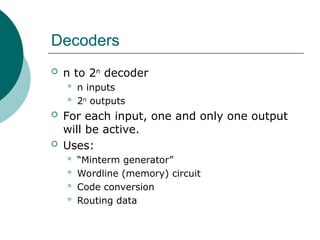
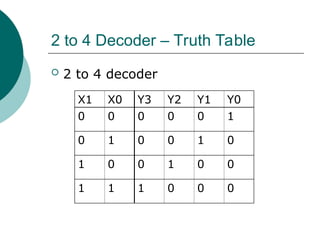
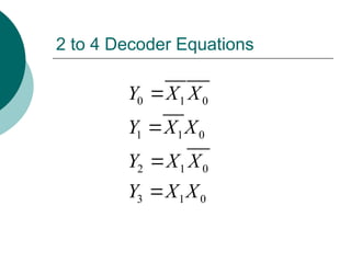
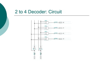
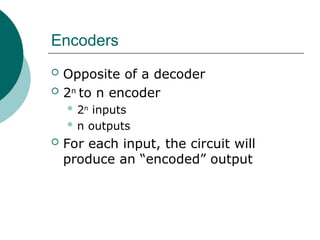
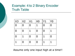
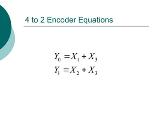
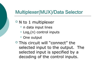
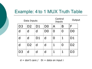
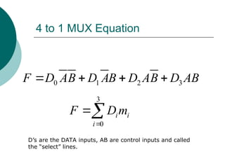
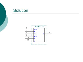
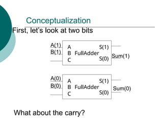
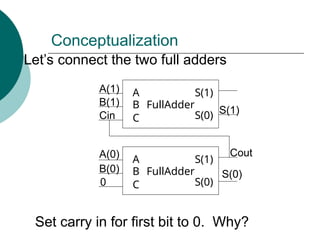
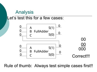
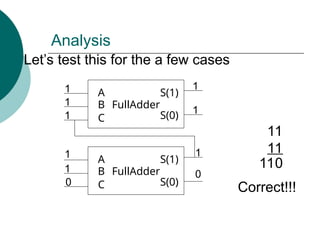
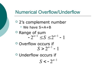
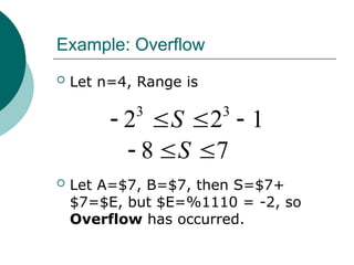
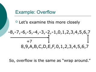
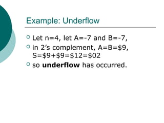
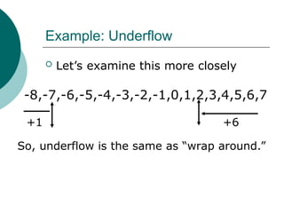
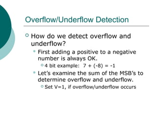
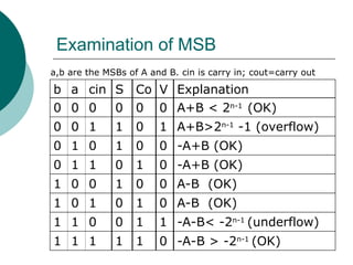
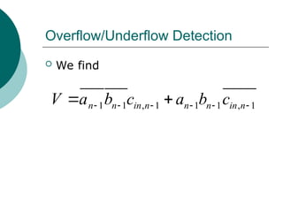
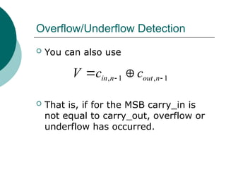
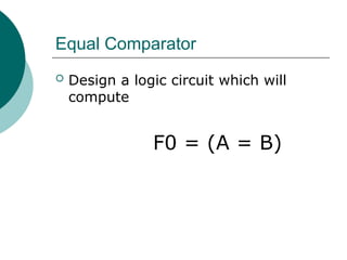
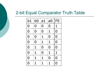
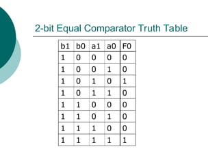
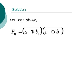
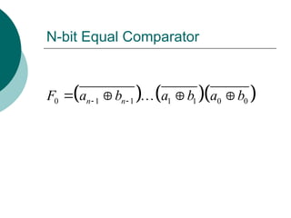
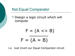
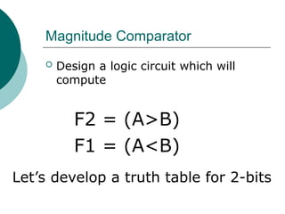
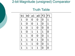
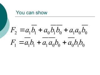
The document discusses modular combinational logic and focuses on decoders, encoders, multiplexers, and demultiplexers. It provides examples, truth tables, and equations for 2 to 4 and 3 to 8 decoders as well as encoders, highlighting their functionalities and circuit designs. Additionally, it explains the role of multiplexers and demultiplexers in data selection and distribution, along with examples of arithmetic elements like half and full adders.


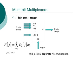
![Example 4-bit 4x1 MUX
A B
D0[3..0]
D1[3..0]
D3[3..0]
D2[3..0]
F[3..0] 4 bits
deep
D0[3..0]
D1[3..0]
D2[3..0]
D3[3..0]
A B
F[3..0]
3
0
i i
i
F j D j m
j=0 to 3 This is just 4 separate 4x1 muxes](https://image.slidesharecdn.com/04chapter4-modularcomblogic-240923044647-62159c6a/85/04_Chapter-4768-Modular-Comb-logic-ppt-52-320.jpg)
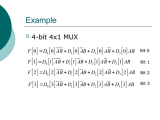
![Example 4 bit 4x1 MUX
For the jth output, we have
D0[j]
D1[j]
D2[j]
D3[j]
A
B
F[j]](https://image.slidesharecdn.com/04chapter4-modularcomblogic-240923044647-62159c6a/85/04_Chapter-4768-Modular-Comb-logic-ppt-54-320.jpg)
![Example 4 bit 4x1 MUX
For the bit 0 output, we have
D0[0]
D1[0]
D2[0]
D3[0]
A
B
F[0]](https://image.slidesharecdn.com/04chapter4-modularcomblogic-240923044647-62159c6a/85/04_Chapter-4768-Modular-Comb-logic-ppt-55-320.jpg)
![Example 4 bit 4x1 MUX
For the bit 1 output, we have
D0[1]
D1[1]
D2[1]
D3[1]
A
B
F[1]](https://image.slidesharecdn.com/04chapter4-modularcomblogic-240923044647-62159c6a/85/04_Chapter-4768-Modular-Comb-logic-ppt-56-320.jpg)
![Example 4 bit 4x1 MUX
For the bit 2 output, we have
D0[2]
D1[2]
D2[2]
D3[2]
A
B
F[2]](https://image.slidesharecdn.com/04chapter4-modularcomblogic-240923044647-62159c6a/85/04_Chapter-4768-Modular-Comb-logic-ppt-57-320.jpg)
![Example 4 bit 4x1 MUX
For the bit 3 output, we have
D0[3]
D1[3]
D2[3]
D3[3]
A
B
F[3]](https://image.slidesharecdn.com/04chapter4-modularcomblogic-240923044647-62159c6a/85/04_Chapter-4768-Modular-Comb-logic-ppt-58-320.jpg)
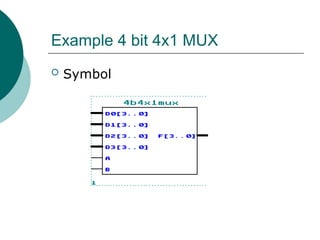
![Example 4 bit 4x1 Mux
F[0]
F[1]
F[2]
F[3]
Complete Circuit
Bit 0
Bit 1
Bit 2
Bit 3](https://image.slidesharecdn.com/04chapter4-modularcomblogic-240923044647-62159c6a/85/04_Chapter-4768-Modular-Comb-logic-ppt-59-320.jpg)


![Arithmetic Logic Unit (ALU)
ALU
A[n-1,,0]
B[n-1..0]
F
S[m-1..0]
A,B are data inputs of n bits each in depth
S is a control input. We have 2m
operations
F is the output](https://image.slidesharecdn.com/04chapter4-modularcomblogic-240923044647-62159c6a/85/04_Chapter-4768-Modular-Comb-logic-ppt-129-320.jpg)
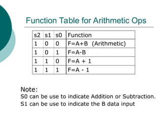
![Example
Let n=4,m=3
We have A[3..0] and B[3..0]
With m=3, we have 23
= 8 operations
Let’s look at a possible function table](https://image.slidesharecdn.com/04chapter4-modularcomblogic-240923044647-62159c6a/85/04_Chapter-4768-Modular-Comb-logic-ppt-130-320.jpg)
![Design using a Truth Table
How large is the truth table?
2n from data inputs A and B
Example: n=8, we have 16 data inputs
A[7..0] and B[7..0]
3 control inputs
Total of 2n+3 inputs
N=8, we have 19 inputs
Our truth table will have
192
(361) rows and 8 outputs
Too complex. Let’s explore another
alternative using a “system” or modular
approach](https://image.slidesharecdn.com/04chapter4-modularcomblogic-240923044647-62159c6a/85/04_Chapter-4768-Modular-Comb-logic-ppt-132-320.jpg)
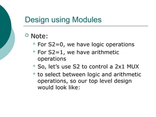
![ALU Design
Logic
Module
Arithmetic
Module
2x1
MUX
S[2]
A B
A
A
B
F
A
B
F
S[1..0]
S[1..0]
B
F F](https://image.slidesharecdn.com/04chapter4-modularcomblogic-240923044647-62159c6a/85/04_Chapter-4768-Modular-Comb-logic-ppt-134-320.jpg)
![ALU Design S2=0
Logic
Module
Arithmetic
Module
2x1
MUX
S[2]
A B
A
A
B
F
A
B
F
S[1..0]
S[1..0]
B
F F
With S2=0, F is the output from
the logic module](https://image.slidesharecdn.com/04chapter4-modularcomblogic-240923044647-62159c6a/85/04_Chapter-4768-Modular-Comb-logic-ppt-135-320.jpg)
![ALU Design S2=1
Logic
Module
Arithmetic
Module
2x1
MUX
S[2]
A B
A
A
B
F
A
B
F
S[1..0]
S[1..0]
B
F F
With S2=1, F is the output from
the arithmetic module](https://image.slidesharecdn.com/04chapter4-modularcomblogic-240923044647-62159c6a/85/04_Chapter-4768-Modular-Comb-logic-ppt-136-320.jpg)
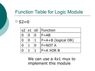
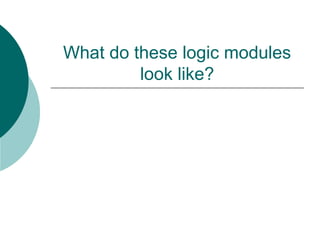
![Logic Module Design
OR
NOT
XOR
AND
A
B
C
D
4
X
1
F
S[1..0]
S1 S0
A
A
B
F
A
B
F
A
B
F
A F
B](https://image.slidesharecdn.com/04chapter4-modularcomblogic-240923044647-62159c6a/85/04_Chapter-4768-Modular-Comb-logic-ppt-139-320.jpg)
![Logic Module Design
OR
NOT
XOR
AND
A
B
C
D
4
X
1
F
S[1..0]
S1 S0
A
A
B
F
A
B
F
A
B
F
A F
B
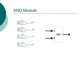
AND Operation
S[1..0]=00
0 0
F=AB](https://image.slidesharecdn.com/04chapter4-modularcomblogic-240923044647-62159c6a/85/04_Chapter-4768-Modular-Comb-logic-ppt-140-320.jpg)
![Logic Module Design
OR
NOT
XOR
AND
A
B
C
D
4
X
1
F
S[1..0]
S1 S0
A
A
B
F
A
B
F
A
B
F
A F
B
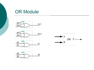
OR Operation
S[1..0]=01
0 1
F=A+B](https://image.slidesharecdn.com/04chapter4-modularcomblogic-240923044647-62159c6a/85/04_Chapter-4768-Modular-Comb-logic-ppt-141-320.jpg)
![Logic Module Design
OR
NOT
XOR
AND
A
B
C
D
4
X
1
F
S[1..0]
S1 S0
A
A
B
F
A
B
F
A
B
F
A F
B
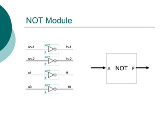
NOT Operation
S[1..0]=10
1 0
F=A](https://image.slidesharecdn.com/04chapter4-modularcomblogic-240923044647-62159c6a/85/04_Chapter-4768-Modular-Comb-logic-ppt-142-320.jpg)
![Logic Module Design
OR
NOT
XOR
AND
A
B
C
D
4
X
1
F
S[1..0]
S1 S0
A
A
B
F
A
B
F
A
B
F
A F
B
XOR Operation
S[1..0]=11
1 1
F=A XOR B](https://image.slidesharecdn.com/04chapter4-modularcomblogic-240923044647-62159c6a/85/04_Chapter-4768-Modular-Comb-logic-ppt-143-320.jpg)
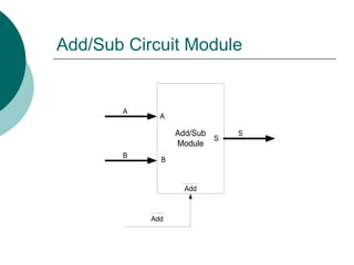

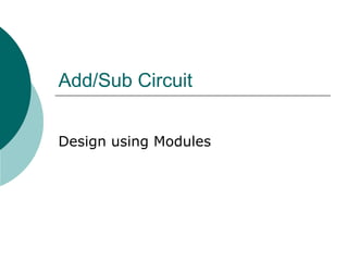
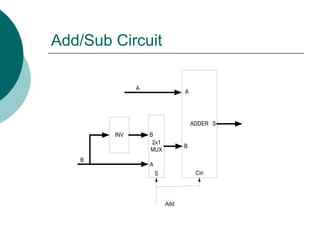
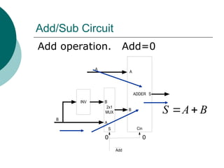
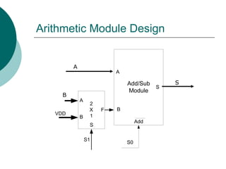
![Arithmetic Module Design
Add/Sub
Module
S0
A
B
Add
S
S
2
X
1
A
B
F
VDD
S1
B
A
S
0
0
F=A+B
S[1..0]=00](https://image.slidesharecdn.com/04chapter4-modularcomblogic-240923044647-62159c6a/85/04_Chapter-4768-Modular-Comb-logic-ppt-153-320.jpg)
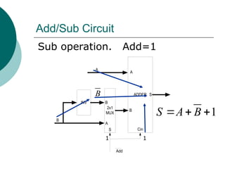
![Arithmetic Module Design
Add/Sub
Module
S0
A
B
Add
S
S
2
X
1
A
B
F
VDD
S1
B
A
S
1
0
F=A-B
S[1..0]=01](https://image.slidesharecdn.com/04chapter4-modularcomblogic-240923044647-62159c6a/85/04_Chapter-4768-Modular-Comb-logic-ppt-154-320.jpg)
![Arithmetic Module Design
Add/Sub
Module
S0
A
B
Add
S
S
2
X
1
A
B
F
VDD
S1
B
A
S
0
1
F=A+1
S[1..0]=10](https://image.slidesharecdn.com/04chapter4-modularcomblogic-240923044647-62159c6a/85/04_Chapter-4768-Modular-Comb-logic-ppt-155-320.jpg)
![Arithmetic Module Design
Add/Sub
Module
S0
A
B
Add
S
S
2
X
1
A
B
F
VDD
S1
B
A
S
1
1
F=A-1
S[1..0]=11](https://image.slidesharecdn.com/04chapter4-modularcomblogic-240923044647-62159c6a/85/04_Chapter-4768-Modular-Comb-logic-ppt-156-320.jpg)

![ALU Design
Logic
Module
Arithmetic
Module
2x1
MUX
S[2]
A B
A
A
B
F
A
B
F
S[1..0]
S[1..0]
B
F F](https://image.slidesharecdn.com/04chapter4-modularcomblogic-240923044647-62159c6a/85/04_Chapter-4768-Modular-Comb-logic-ppt-158-320.jpg)
![Logic Module Design
OR
NOT
XOR
AND
A
B
C
D
4
X
1
F
S[1..0]
S1 S0
A
A
B
F
A
B
F
A
B
F
A F
B](https://image.slidesharecdn.com/04chapter4-modularcomblogic-240923044647-62159c6a/85/04_Chapter-4768-Modular-Comb-logic-ppt-159-320.jpg)
![Total Design
OR
NOT
XOR
AND
A
B
C
D
4
X
1
F
S[1..0]
Add/Sub
Module
A
S
S0
A
B
Add
S
B
S
F
2
X
1
S2
S
2
X
1
A
B
F
VDD
S1 S0
S1
A B
A
B
F
A
B
F
A
B
F
A F
Logic Module
Arithmetic Module](https://image.slidesharecdn.com/04chapter4-modularcomblogic-240923044647-62159c6a/85/04_Chapter-4768-Modular-Comb-logic-ppt-161-320.jpg)