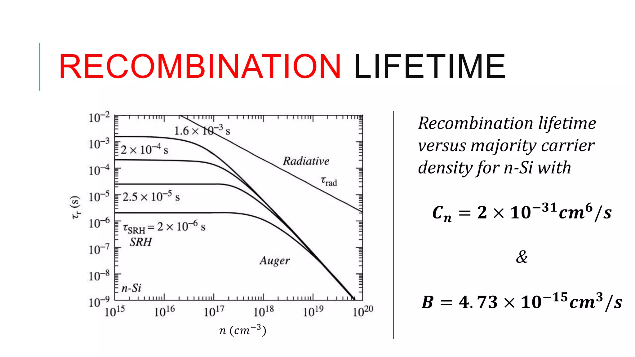
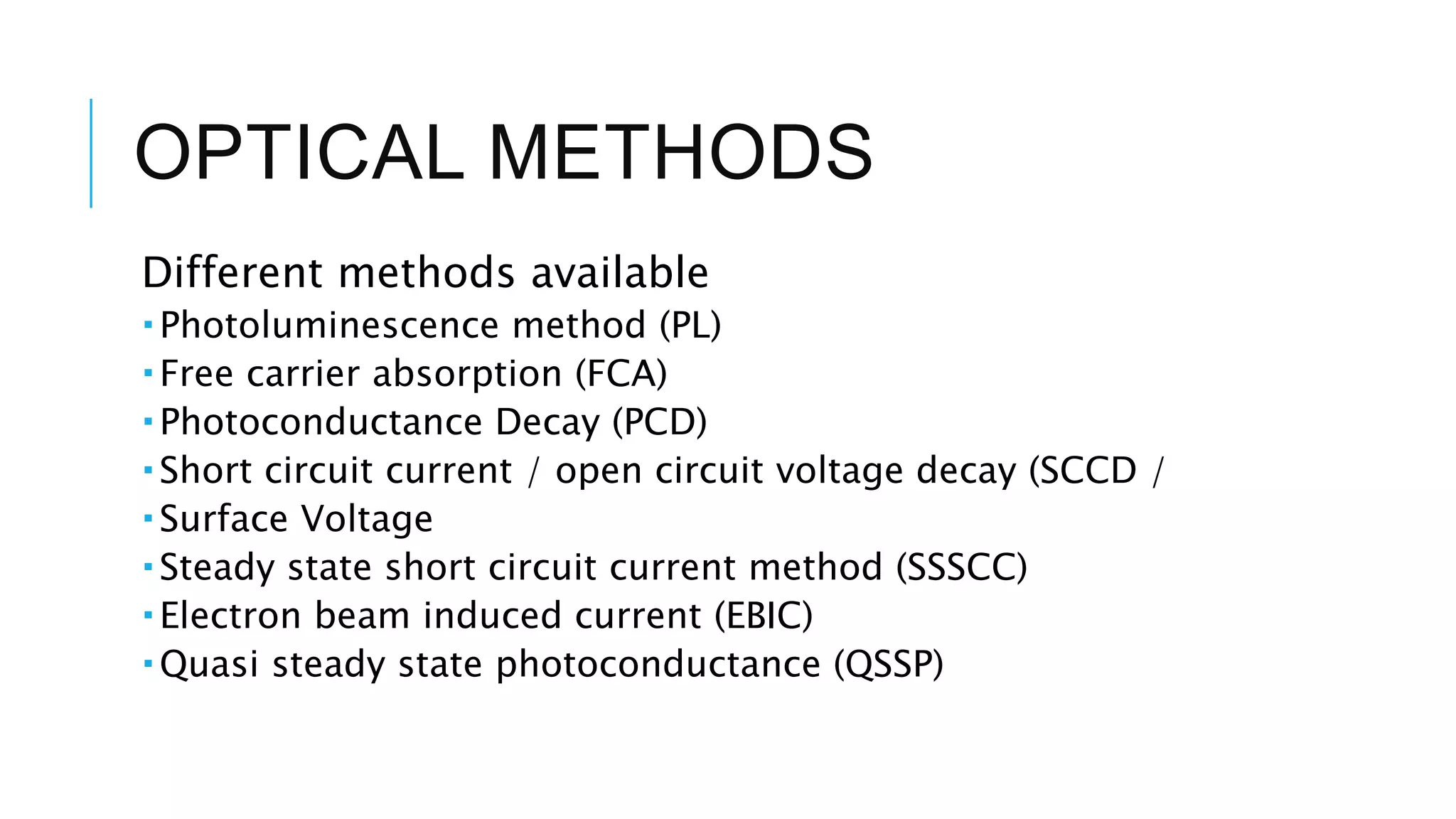
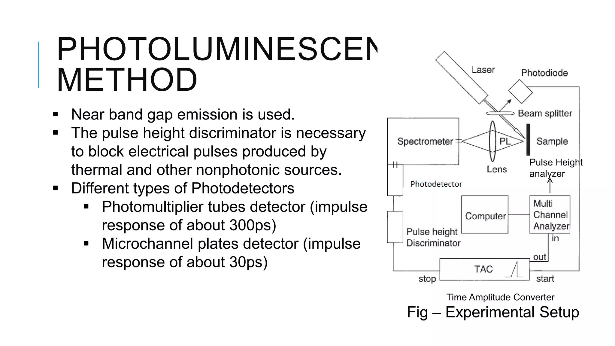
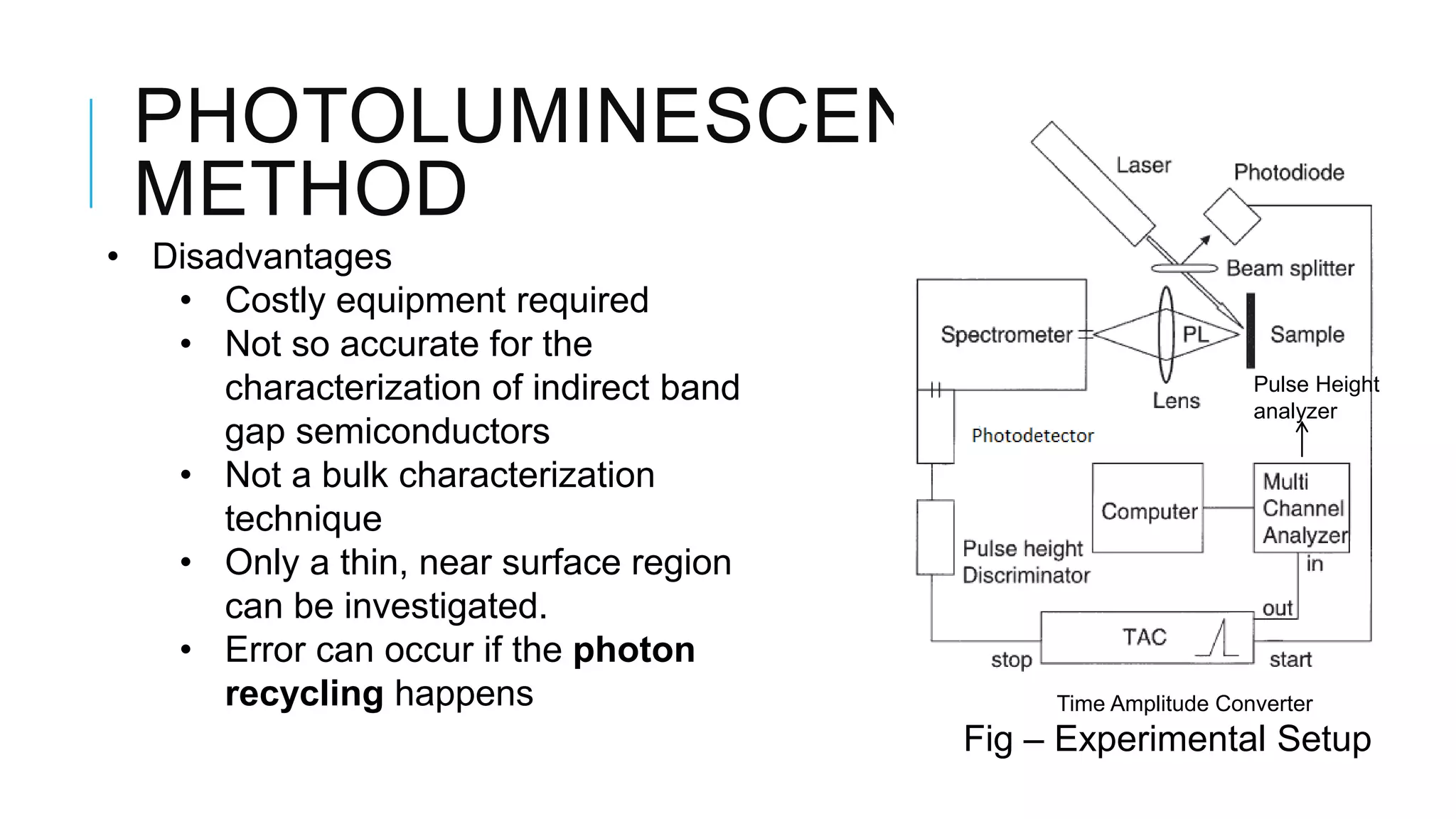
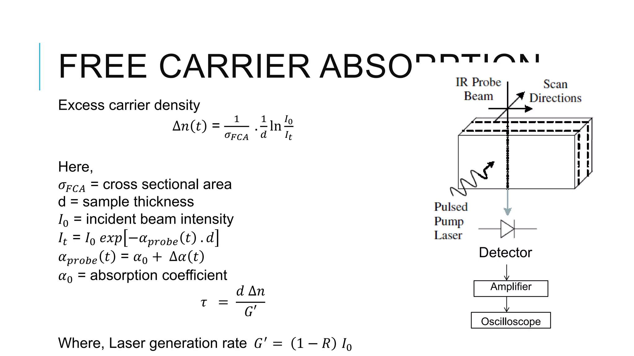
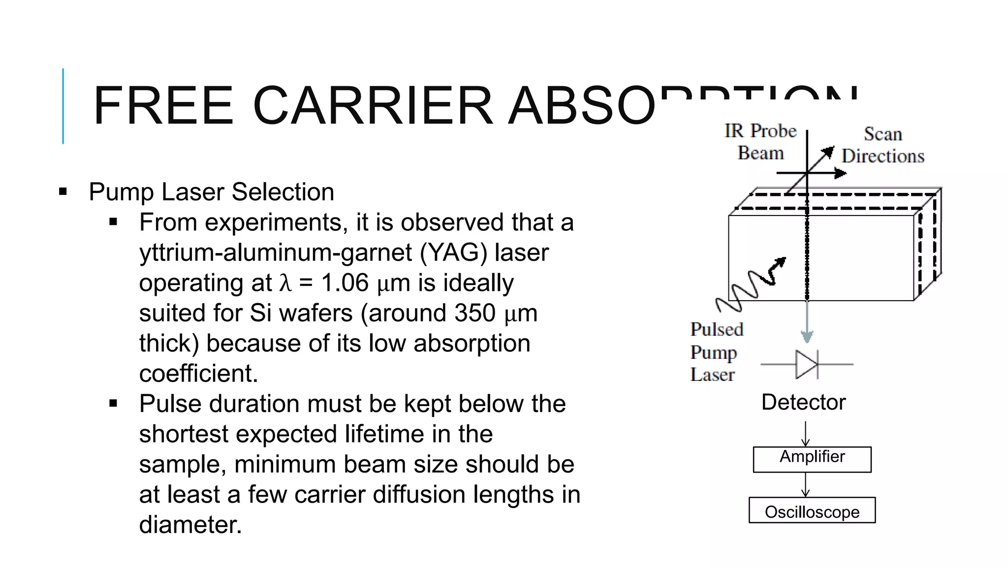
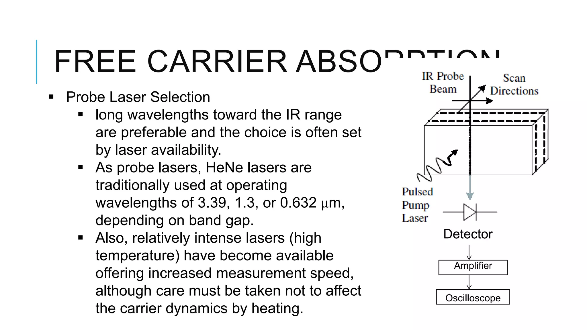
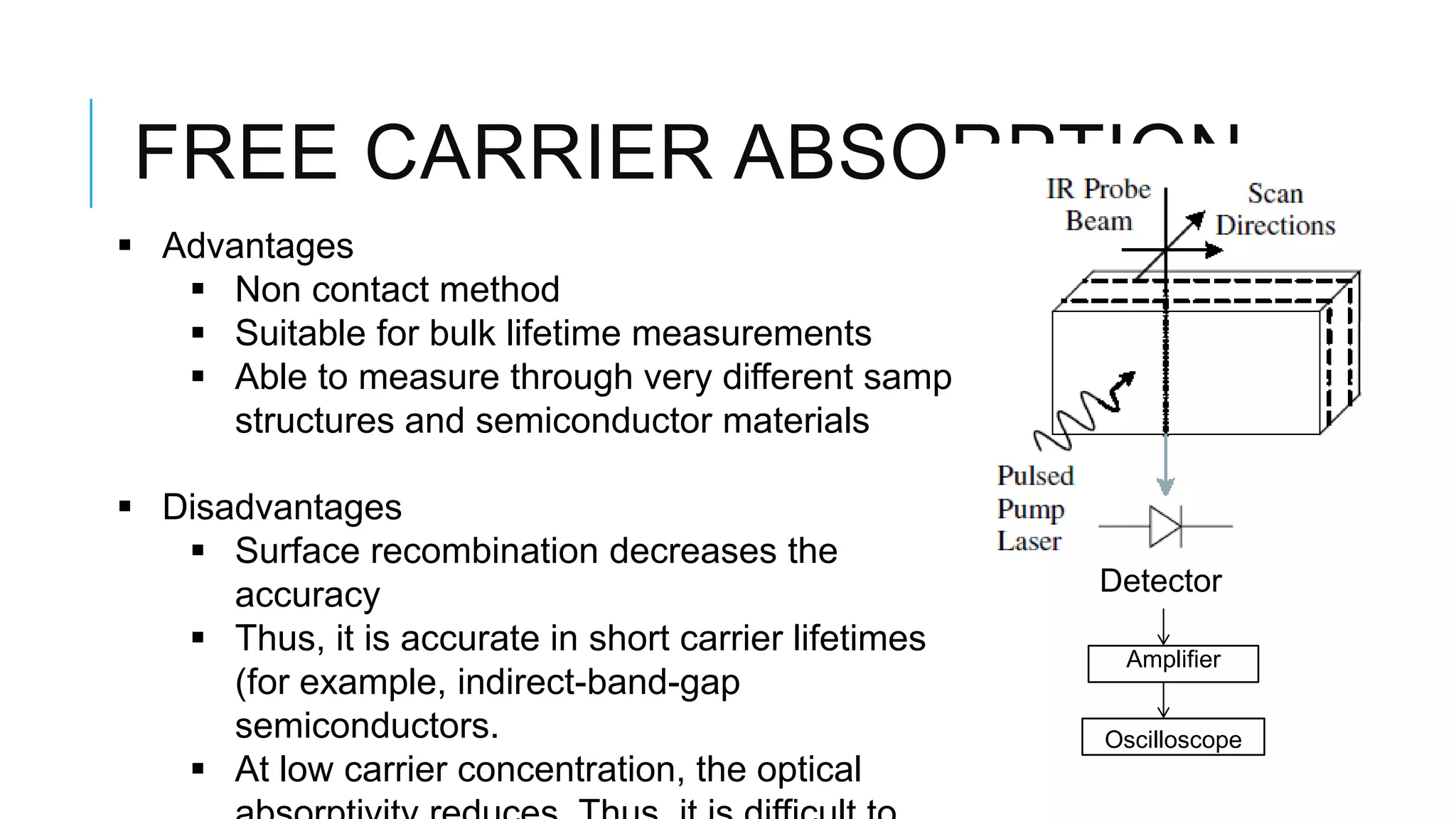
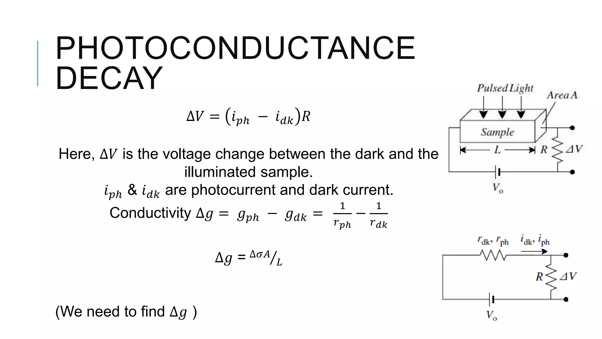
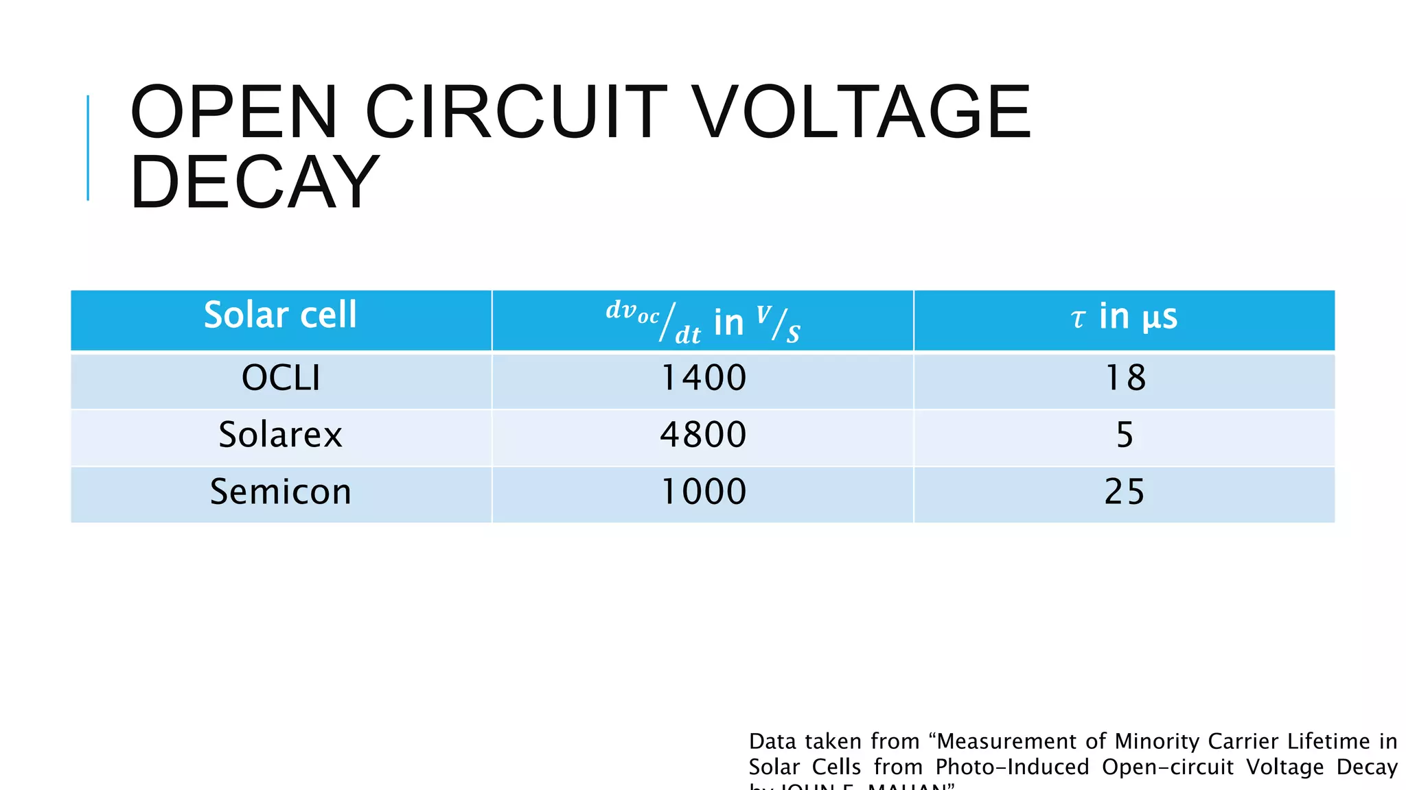
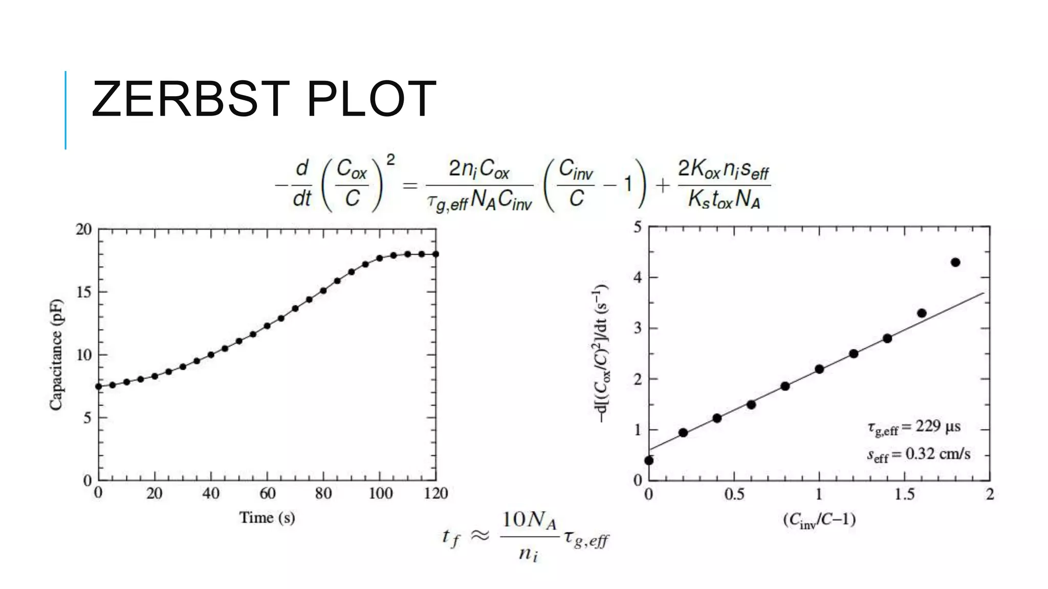
This document provides an overview of carrier lifetime characterization techniques. It discusses that carrier lifetime determines the performance of semiconductor devices and solar cells. It then defines recombination lifetime and generation lifetime. The document proceeds to describe various optical methods to measure carrier lifetime, including photoluminescence, free carrier absorption, photoconductance decay, and their advantages and disadvantages. It provides equations to calculate carrier lifetime from measurements of excess carrier density, conductivity change, and voltage change.
Hello, I am Subhajit Pramanick. I and my classmate, Anannya Sahaw, both presented this ppt in seminar of our Institute, Indian Institute of Technology, Kharagpur. The topic of this presentation is on exchange interaction and their consequences. It includes the basic of exchange interaction, the origin of it, classification of it and their discussions etc. We hope you will all enjoy by reading this presentation. Thank you.
Research proposal on organic-inorganic halide perovskite light harvesting mat...Rajan K. Singh
Organic-Inorganic perovskite materials has many applications in the field of opto-electronics such as photo-voltaic cells, LEDs, sensors, memory devices etc. due to its excellent optical and electrical properties. Presence of Pb in such type of perovskite is the biggest challenge for researchers.
For free download Subscribe to https://www.youtube.com/channel/UCTfiZ8qwZ_8_vTjxeCB037w and Follow https://www.instagram.com/fitrit_2405/ then please contact +91-9045839849 over WhatsApp.
Graphene Presentation
This PPT gives introduction
to Dielectrics, Piezoelectrics & Ferroelectrics Materials, Methods and Applications. A quick glance at the dielectric phenomena, symmetry, classification, modelling, figures of merit and applications.
Comprehensive overview of the physics and applications of
ferroelectric
This presentation summarizes history and recent development of perovskite solar cells. If you have any questions or comments, you can reach me at agassifeng@gmail.com
Quantum Dot Light Emitting Diode
Introduction
Quantum dots (QD) or semiconductor Nano crystals could provide an alternative for commercial applications such as display technology. This display technology would be similar to organic light-emitting diode (OLED) displays, in that light would be supplied on demand, which would enable more efficient displays.
Quantum dots could support large, flexible displays. At present, they are used only to filter light from LEDs to backlight LCDs, rather than as actual displays. Properties and performance are determined by the size and/or composition of the QD. QDs are both photo-active (photo luminescent) and electro-active (electroluminescent) allowing them to be readily incorporated into new emissive display architectures.
Definition
QD-LED or QLED is considered as a next generation display technology after OLED-Displays.
“QLED means Quantum dot light emitting diodes and are a form of light emitting technology and consist of nano-scale crystals that can provide an alternative for applications such as display technology”. The light emitting centers are cadmium selenide (CdSe) nanocrystals, or quantum dots.
Charactristics
❀ QLEDs are a reliable, energy efficient, tunable color solution for display and lighting applications that reduce manufacturing costs, while employing ultra-thin, transparent or flexible materials.
❀ Quantum-dot-based LEDs are characterized by pure and saturated emission colors with narrow bandwidth.
❀ Their emission wavelength is easily tuned by changing the size of the quantum dots. Moreover, QD-LED offer high color purity and durability combined with the efficiency, flexibility, and low processing cost of organic light-emitting devices. QD-LED structure can be tuned over the entire visible wavelength range from 460 nm (blue) to 650 nm
❀ Due to spectrally narrow, tunable emission, and ease of processing, colloidal QDs are attractive materials for LED technologies.
Optical band gap measurement by diffuse reflectance spectroscopy (drs)Sajjad Ullah
Introduction to Optical band gap measurement
by electronic spectroscopy and diffuse reflectance spectroscopy (DRS) with comparison of the results obtained suing different equation and measurement techniques.
The role of scattering in extinction of light as it passes through media is briefly discussed.
These slides present the results from the thesis with the same name as the presentation title. It deals with operational aspects of superconducting (SC) accelerating cavities related to charging the same. It proposes an optimal scheme to charge the SC cavities such that the total reflected energy is minimised. Following which it presents a way of extending the well known Q-circle method to SC cavities for accurate estimation of cavity quality factor (Q0). The measurements reveal the effect of cool down on cavity Q0. Present literature proposed the effect of trapped magnetic field in surface impurities. In the thesis I use the Ginzburg-Landau model of superconductivity to theoretically explain the effect of magnetic field, impurity and temperature gradient. This allows a theoretical model that explains the experimental results.
Dual-hop Variable-Gain Relaying with Beamforming over 휿−흁 Shadowed Fading Cha...zeenta zeenta
Dual-hop relaying with beamforming is studied under 휅−휇 shadowed fading environments. Exact and asymptotic results for the outage probability and average capacity are derived.
Effects of shadowing on the system performance are analyzed in different scenarios
The analysis results is general that it includes many special cases.
Simulation Of Algan/Si And Inn/Si Electric - Devicesijrap
In this work, efficient solar-blind metal-semiconductor photodetectors grown on Si (111) by
molecular beam epitaxy are reported. Growth details are described,the comparison enters the
properties electric of InN/Si and AlGaN/Si photodectors with 0.2 µm of AlGaN and InN layers.
Modeling and simulation were performed by using ATLAS-TCAD simulator. Energy band
diagram, doping profile, conduction current density,I-V caracteristic , internal potential and
electric field were performed.
Simulation of AlGaN/Si and InN/Si ELECTRIC –DEVICESijrap
In this work, efficient solar-blind metal-semiconductor photodetectors grown on Si (111) by
molecular beam epitaxy are reported. Growth details are described,the comparison enters the
properties electric of InN/Si and AlGaN/Si photodectors with 0.2 μm of AlGaN and InN layers.
Modeling and simulation were performed by using ATLAS-TCAD simulator. Energy band
diagram, doping profile, conduction current density,I-V caracteristic , internal potential and
electric field were performed.
Simulation of AlGaN/Si and InN/Si ELECTRIC –DEVICESijrap
In this work, efficient solar-blind metal-semiconductor photodetectors grown on Si (111) by
molecular beam epitaxy are reported. Growth details are described,the comparison enters the
properties electric of InN/Si and AlGaN/Si photodectors with 0.2 µm of AlGaN and InN layers.
Modeling and simulation were performed by using ATLAS-TCAD simulator. Energy band
diagram, doping profile, conduction current density,I-V caracteristic , internal potential and
electric field were performed
Design of metamaterial absorber using eight resistive-arm cell for simultaneo...Tuấn Tạ Minh
In this paper, a broadband metamaterial (MM) absorber is presented for X-band applications. A novel eight resistive-arm (ERA) cell is proposed as an MM unit cell to achieve both broadband absorption and wide incidence angles. The proposed ERA cell is designed using equivalent circuit model and full- wave analysis in order to achieve an absorption ratio higher than 90% in the range of 8.2–13.4 GHz. The experimental results indicate that the absorptivity was greater than 90% in the range of 8–13 GHz for all polarization angles under normal incidence. Under oblique incidence, the measured absorptivity was greater than 90% in the range of 8.2–12.2 GHz up to 60° and in the range of 9.2–12 GHz up to 65° in the transverse electric (TE) mode. In the transverse magnetic (TM) mode, the measured absorptivity was higher than 90% in the range of 9.5–12.4 GHz when the incidence angle was varied from 0° to 60° and remaining a 90% absorption bandwidth in the range of 10–12 GHz up to 65°. Compared to other broadband MM absorbers, the proposed MM absorber exhibited the widest incidence angles in both TE and TM modes.
- Basic overview of transmission line analysis
-How transmission line analysis differs from basic circuit analysis
- How distributed circuit element differs from Lumped elements
-Links to be referred for Smith Chart
Efficiency Improvement of p-i-n Structure over p-n Structure and Effect of p-...iosrjce
IOSR Journal of Applied Physics (IOSR-JAP) is a double blind peer reviewed International Journal that provides rapid publication (within a month) of articles in all areas of physics and its applications. The journal welcomes publications of high quality papers on theoretical developments and practical applications in applied physics. Original research papers, state-of-the-art reviews, and high quality technical notes are invited for publications.
Designing Class a Colpitts Oscillator and Analyzing the Effect of DC Power Su...ijtsrd
Oscillator circuit is one that converts DC power into AC power at a frequency without any input signal. Oscillators are commonly used in communication systems to generate carrier frequency ranging from audio frequency 20 Hz to radio frequency 100G Hz . There are two main classes of oscillators, harmonic oscillator with sinusoidal output e.g. sine wave and relaxation oscillator with non sinusoidal output e.g. square wave, triangle wave, etc. . In this paper, class A Colpitts oscillator with LC feedback circuit is designed as a radio frequency oscillator to generate the output signals at 5M Hz. After designing, this circuit is simulated with Multisim software to analyze the effect of power supply on its frequency stability. Three supply voltages, 14 V, 12 V and 10 V are set as sample parameters to analyze the variation of frequency and voltage of the output signal. Changing DC power supply one by one as the above selected parameters in Multisim, the change of value of frequencies are noted and output signal results are also shown with the help of virtual oscillator. Thit Waso Khine "Designing Class a Colpitts Oscillator and Analyzing the Effect of DC Power Supply on its Frequency Stability" Published in International Journal of Trend in Scientific Research and Development (ijtsrd), ISSN: 2456-6470, Volume-3 | Issue-5 , August 2019, URL: https://www.ijtsrd.com/papers/ijtsrd28022.pdfPaper URL: https://www.ijtsrd.com/engineering/electronics-and-communication-engineering/28022/designing-class-a-colpitts-oscillator-and-analyzing-the-effect-of-dc-power-supply-on-its-frequency-stability/thit-waso-khine
Similar to Characterization of Carrier Lifetime (20)
Introduction to AI for Nonprofits with Tapp NetworkTechSoup
Dive into the world of AI! Experts Jon Hill and Tareq Monaur will guide you through AI's role in enhancing nonprofit websites and basic marketing strategies, making it easy to understand and apply.
Macroeconomics- Movie Location
This will be used as part of your Personal Professional Portfolio once graded.
Objective:
Prepare a presentation or a paper using research, basic comparative analysis, data organization and application of economic information. You will make an informed assessment of an economic climate outside of the United States to accomplish an entertainment industry objective.
Operation “Blue Star” is the only event in the history of Independent India where the state went into war with its own people. Even after about 40 years it is not clear if it was culmination of states anger over people of the region, a political game of power or start of dictatorial chapter in the democratic setup.
The people of Punjab felt alienated from main stream due to denial of their just demands during a long democratic struggle since independence. As it happen all over the word, it led to militant struggle with great loss of lives of military, police and civilian personnel. Killing of Indira Gandhi and massacre of innocent Sikhs in Delhi and other India cities was also associated with this movement.
Welcome to TechSoup New Member Orientation and Q&A (May 2024).pdfTechSoup
In this webinar you will learn how your organization can access TechSoup's wide variety of product discount and donation programs. From hardware to software, we'll give you a tour of the tools available to help your nonprofit with productivity, collaboration, financial management, donor tracking, security, and more.
Biological screening of herbal drugs: Introduction and Need for
Phyto-Pharmacological Screening, New Strategies for evaluating
Natural Products, In vitro evaluation techniques for Antioxidants, Antimicrobial and Anticancer drugs. In vivo evaluation techniques
for Anti-inflammatory, Antiulcer, Anticancer, Wound healing, Antidiabetic, Hepatoprotective, Cardio protective, Diuretics and
Antifertility, Toxicity studies as per OECD guidelines
Embracing GenAI - A Strategic ImperativePeter Windle
Artificial Intelligence (AI) technologies such as Generative AI, Image Generators and Large Language Models have had a dramatic impact on teaching, learning and assessment over the past 18 months. The most immediate threat AI posed was to Academic Integrity with Higher Education Institutes (HEIs) focusing their efforts on combating the use of GenAI in assessment. Guidelines were developed for staff and students, policies put in place too. Innovative educators have forged paths in the use of Generative AI for teaching, learning and assessments leading to pockets of transformation springing up across HEIs, often with little or no top-down guidance, support or direction.
This Gasta posits a strategic approach to integrating AI into HEIs to prepare staff, students and the curriculum for an evolving world and workplace. We will highlight the advantages of working with these technologies beyond the realm of teaching, learning and assessment by considering prompt engineering skills, industry impact, curriculum changes, and the need for staff upskilling. In contrast, not engaging strategically with Generative AI poses risks, including falling behind peers, missed opportunities and failing to ensure our graduates remain employable. The rapid evolution of AI technologies necessitates a proactive and strategic approach if we are to remain relevant.
Unit 8 - Information and Communication Technology (Paper I).pdfThiyagu K
This slides describes the basic concepts of ICT, basics of Email, Emerging Technology and Digital Initiatives in Education. This presentations aligns with the UGC Paper I syllabus.
2024.06.01 Introducing a competency framework for languag learning materials ...Sandy Millin
http://sandymillin.wordpress.com/iateflwebinar2024
Published classroom materials form the basis of syllabuses, drive teacher professional development, and have a potentially huge influence on learners, teachers and education systems. All teachers also create their own materials, whether a few sentences on a blackboard, a highly-structured fully-realised online course, or anything in between. Despite this, the knowledge and skills needed to create effective language learning materials are rarely part of teacher training, and are mostly learnt by trial and error.
Knowledge and skills frameworks, generally called competency frameworks, for ELT teachers, trainers and managers have existed for a few years now. However, until I created one for my MA dissertation, there wasn’t one drawing together what we need to know and do to be able to effectively produce language learning materials.
This webinar will introduce you to my framework, highlighting the key competencies I identified from my research. It will also show how anybody involved in language teaching (any language, not just English!), teacher training, managing schools or developing language learning materials can benefit from using the framework.
The Roman Empire A Historical Colossus.pdfkaushalkr1407
The Roman Empire, a vast and enduring power, stands as one of history's most remarkable civilizations, leaving an indelible imprint on the world. It emerged from the Roman Republic, transitioning into an imperial powerhouse under the leadership of Augustus Caesar in 27 BCE. This transformation marked the beginning of an era defined by unprecedented territorial expansion, architectural marvels, and profound cultural influence.
The empire's roots lie in the city of Rome, founded, according to legend, by Romulus in 753 BCE. Over centuries, Rome evolved from a small settlement to a formidable republic, characterized by a complex political system with elected officials and checks on power. However, internal strife, class conflicts, and military ambitions paved the way for the end of the Republic. Julius Caesar’s dictatorship and subsequent assassination in 44 BCE created a power vacuum, leading to a civil war. Octavian, later Augustus, emerged victorious, heralding the Roman Empire’s birth.
Under Augustus, the empire experienced the Pax Romana, a 200-year period of relative peace and stability. Augustus reformed the military, established efficient administrative systems, and initiated grand construction projects. The empire's borders expanded, encompassing territories from Britain to Egypt and from Spain to the Euphrates. Roman legions, renowned for their discipline and engineering prowess, secured and maintained these vast territories, building roads, fortifications, and cities that facilitated control and integration.
The Roman Empire’s society was hierarchical, with a rigid class system. At the top were the patricians, wealthy elites who held significant political power. Below them were the plebeians, free citizens with limited political influence, and the vast numbers of slaves who formed the backbone of the economy. The family unit was central, governed by the paterfamilias, the male head who held absolute authority.
Culturally, the Romans were eclectic, absorbing and adapting elements from the civilizations they encountered, particularly the Greeks. Roman art, literature, and philosophy reflected this synthesis, creating a rich cultural tapestry. Latin, the Roman language, became the lingua franca of the Western world, influencing numerous modern languages.
Roman architecture and engineering achievements were monumental. They perfected the arch, vault, and dome, constructing enduring structures like the Colosseum, Pantheon, and aqueducts. These engineering marvels not only showcased Roman ingenuity but also served practical purposes, from public entertainment to water supply.
1. Characterization of Carrier
Lifetime
Presentation as part of internal assessment in course
Semiconductor Processing & Characterization
M.Tech Solar, PDPU.
Presented to
Prof. Manoj Kumar
Presented by
Aditya Soni
(17MSE001)
Jay Joshi
(17MSE005)
Mrunmayee Unawane
(17MSE016)
2. CARRIER LIFETIMES – WHY
MEASURE THEM
In IC Industries,
• Carrier lifetime determines
performance of devices.
• It is a sensitive measure of
material quality and
cleanliness.
• It gives information about
defect densities as low as
to 1o11 cm-3
8/18/2018
In Solar Cells,
•Carrier lifetime of minority
carriers determines
performance of the solar cell.
•Longer the minority carries
retain the energy
corresponding to the
conduction band, higher their
probability to cross the SCR
and contribute in conduction.
Band diagram of Solar
Cell under illumination.
3. ℎ𝜈
CARRIER LIFETIMES – WHAT
ARE THEY
Recombination lifetime
𝜏 𝑟:
Excess carriers decay by
recombining
𝜏 𝑟 is the average time after
which the electron goes
back in the valence band
and recombines with it’s
hole.
8/18/2018
E
v
Ec
𝑛𝑜𝑛 𝑟𝑎𝑑𝑖𝑎𝑡𝑖𝑣𝑒 𝑒𝑚𝑚𝑖𝑠𝑖𝑜𝑛
𝑅−𝐺 𝐶𝑒𝑛𝑡𝑒𝑟𝑠
E
v
Ec
• Band to Band recombination
• SRH Recombination
• Auger recombination
E
v
Ec
4. CARRIER LIFETIMES – WHAT
ARE THEY
Generation lifetime 𝜏 𝑔:
In case of lack of carriers,
electron-hole pairs are
generated.
𝜏 𝑔 is the average time
which the electron hole
is generated.
Misnomer - Generation
Time.
8/18/2018
• Thermal Generation
• Optical Generation
• Impact Ionization
generation
E
v
Ec
Ef
T = o K T > o K
E
v
Ec
ℎ𝜈 > 𝐸 𝑔
An carrier with enough
kinetic energy can knock
a bound electron out of
its bound state and
promote it to a state in
the conduction band,
creating an electron-hole
pair.
9. OPTICAL METHODS
Different methods available
Photoluminescence method (PL)
Free carrier absorption (FCA)
Photoconductance Decay (PCD)
Short circuit current / open circuit voltage decay (SCCD /
Surface Voltage
Steady state short circuit current method (SSSCC)
Electron beam induced current (EBIC)
Quasi steady state photoconductance (QSSP)
10. PHOTOLUMINESCENCE
METHOD
Near band gap emission is used.
The pulse height discriminator is necessary
to block electrical pulses produced by
thermal and other nonphotonic sources.
Different types of Photodetectors
Photomultiplier tubes detector (impulse
response of about 300ps)
Microchannel plates detector (impulse
response of about 30ps)
Fig – Experimental Setup
Time Amplitude Converter
Pulse Height
analyzer
11. PHOTOLUMINESCENCE
METHOD
• Advantages
• Non contact method
• Also can be used for
determining the composition of
compound Semiconductors,
such as 𝐴𝑙 𝑥 𝐺𝑎1−𝑥 𝐴𝑠 by using
shallow emission or deep level
emissions
Fig – Experimental Setup
Time Amplitude Converter
Pulse Height
analyzer
12. PHOTOLUMINESCENCE
METHOD
• Disadvantages
• Costly equipment required
• Not so accurate for the
characterization of indirect band
gap semiconductors
• Not a bulk characterization
technique
• Only a thin, near surface region
can be investigated.
• Error can occur if the photon
recycling happens
Fig – Experimental Setup
Time Amplitude Converter
Pulse Height
analyzer
13. PHOTON RECYCLING
Basically, it is the recapturing of photon
It may give you the carrier lifetime well above the theoretical value
It could be corrected by adding the photon recycling factor in the final
equation
ℎ𝜈
E
v
Ec
15. FREE CARRIER ABSORPTION
Detector
Pump Laser Selection
From experiments, it is observed that a
yttrium-aluminum-garnet (YAG) laser
operating at λ = 1.06 μm is ideally
suited for Si wafers (around 350 μm
thick) because of its low absorption
coefficient.
Pulse duration must be kept below the
shortest expected lifetime in the
sample, minimum beam size should be
at least a few carrier diffusion lengths in
diameter.
Amplifier
Oscilloscope
16. FREE CARRIER ABSORPTION
Probe Laser Selection
long wavelengths toward the IR range
are preferable and the choice is often set
by laser availability.
As probe lasers, HeNe lasers are
traditionally used at operating
wavelengths of 3.39, 1.3, or 0.632 μm,
depending on band gap.
Also, relatively intense lasers (high
temperature) have become available
offering increased measurement speed,
although care must be taken not to affect
the carrier dynamics by heating.
Detector
Amplifier
Oscilloscope
17. FREE CARRIER ABSORPTION
Detection Electronics
Reduction of noise is the priority
here.
To reduce noise, oscilloscopes with
minimum bandwidth is selected.
Digital oscilloscope is preferred over
the analog because of the provision
of digital averaging.
Detector
Amplifier
Oscilloscope
18. FREE CARRIER ABSORPTION
Advantages
Non contact method
Suitable for bulk lifetime measurements
Able to measure through very different sample
structures and semiconductor materials
Disadvantages
Surface recombination decreases the
accuracy
Thus, it is accurate in short carrier lifetimes
(for example, indirect-band-gap
semiconductors.
At low carrier concentration, the optical
Detector
Amplifier
Oscilloscope
20. PHOTOCONDUCTANCE
DECAY
Methodology
Conductivity can be given by, 𝜎 = 𝑞 𝜇 𝑛 𝑛 + 𝜇 𝑝 𝑝
Where, 𝜇 𝑛 and 𝜇 𝑝 are the mobility of electrons and holes
q is the charge of electron
n = 𝑛0 + ∆𝑛 & p = 𝑝0 + ∆𝑝
For equilibrium, ∆𝑛 = ∆𝑝
Therefore, ∆𝑛 =
∆𝜎
𝑞 𝜇 𝑛+𝜇 𝑝
(We need to find ∆𝜎)
21. PHOTOCONDUCTANCE
DECAY
∆𝑉 = 𝑖 𝑝ℎ − 𝑖 𝑑𝑘 𝑅
Here, ∆𝑉 is the voltage change between the dark and the
illuminated sample.
𝑖 𝑝ℎ & 𝑖 𝑑𝑘 are photocurrent and dark current.
Conductivity ∆𝑔 = 𝑔 𝑝ℎ − 𝑔 𝑑𝑘 =
1
𝑟 𝑝ℎ
−
1
𝑟 𝑑𝑘
∆𝑔 = ∆𝜎𝐴
𝐿
(We need to find ∆𝑔 )
22. PHOTOCONDUCTANCE
DECAY
∆𝑉 =
𝑅 ∆𝑔 𝑣0 𝑟𝑑𝑘
2
𝑅 + 𝑟𝑑𝑘 (𝑅 + 𝑟𝑑𝑘 + 𝑅𝑟𝑑𝑘∆𝑔)
For constant voltage, the above equation can be written
as
∆𝑉 = 𝑅 ∆𝑔 𝑣0 1 −
∆𝑉
𝑉0
Form this equation, we get ∆𝑔.
23. VERDICT
Versatile techniques. Can be used for several different
conductors.
Non contact method, which means simple or no sample
preparation.
You may get an error in the calculation if carrier trapping
is dominant.
They require comparatively complex experimental setup.
26. OPEN-CIRCUIT VOLTAGE
DECAY (OCVD)
Fig a. Plot of the decay of Voc with time
The carriers decay
exponentially, due to
recombination given by
𝑛 = 𝐴𝑒𝑥𝑝(
−𝑡
𝜏o
)
The open‐circuit voltage
decay (OCVD) goes
approximately as:
𝑉𝑜𝑐 𝑡 = 𝑉𝑜𝑐 o −
𝑘𝑇
𝑞
−𝑡
𝜏o
𝑉𝑜𝑐(𝑡)
𝑉𝑜𝑐(o)
27. The open‐circuit voltage decay (OCVD) goes approximately as:
𝑉𝑜𝑐 𝑡 = 𝑉𝑜𝑐 o −
𝑘𝑇
𝑞
−𝑡
𝜏o
𝜏o =
𝑘𝑇
𝑞
𝑑𝑉𝑜𝑐
𝑑𝑡
−1
Experimental Setup & Output:
Fig b. Circuit diagram for the OCVD
experiment
Fig c. A typical Voc plot when the solar cell is
repeatedly turned ON and OFF
28. OPEN CIRCUIT VOLTAGE
DECAY
Solar cell 𝒅𝒗 𝒐𝒄
𝒅𝒕 in 𝑽
𝑺
𝜏 in μs
OCLI 1400 18
Solarex 4800 5
Semicon 1000 25
Data taken from “Measurement of Minority Carrier Lifetime in
Solar Cells from Photo-Induced Open-circuit Voltage Decay
29. REVERSE RECOVERY (RR)
Fig a. Circuit
Schematic
Fig b. Plot of reverse recovery of a solar cell under
transient condition
V(t)
V(f)
V t
t
i(t) I(f)
-Ir ts𝑡 𝑠 = 𝜏 𝑜ln 1 +
𝐼𝑓
𝐼𝑟
30. CONCEPT OF MOS
CAPACITOR
Fig a: Structure of MOS Capacitor
𝐶 =
𝐶 𝑜𝑥 × 𝐶 𝑑
𝐶 𝑜𝑥 + 𝐶 𝑑
Total Capacitance C is given by,
32. C-V CHARACTERISTICS OF A
MOS STRUCTURE
Characteristic of structure at
a- Low Frequency
b- High Frequency
c- High Frequency with pulsed bias
Methods are based on return of pulsed
MOS to equilibrium from
Accumulation towards depletion
Inversion towards depletion
33. DEEP DEPLETION METHOD
The MOS receives voltage pulses, going from equilibrium to deep
depletion: the capacitance is observed as the MOS comes back to
equilibrium via thermal generation of carriers.
Fig a. The C–VG and C − t behavior of an MOS-C pulsed into
deep depletion.
35. CURRENT-CAPACITANCE
Advantages:
Does not require differentiation of
experimental data
Doping concentration need not be
known
Measurement time required is less
Fig a. Current Vs Inverse
Capacitance Plot
36. CONCLUSIONS
Electrical Measurements methods are technically
simple as they are based on current, voltage and
capacitance methods.
Recombination lifetimes are best measured by optical
methods, while generation lifetimes prefer the MOS
capacitor method, especially for thin layers like
epitaxial layers.
37. The recombination lifetime τr is
shown in Fig. and given by,
1
𝜏 𝑟
=
1
𝜏 𝑅𝑎𝑑
+
1
𝜏 𝑆𝑅𝐻
+
1
𝜏 𝐴𝑢𝑔𝑒𝑟
Determine σpNT and C for device
(i) and σpNT and B for device (ii).
vth = 107 cm/s.
Problem
38. Problem 1
For device (i),
𝜏 𝑆𝑅𝐻 =
1
𝜎 𝑝 𝑣 𝑡ℎ 𝑁𝑡
= 5 × 10⁻⁶
𝑠𝑒𝑐
𝜎 𝑝 𝑣 𝑡ℎ 𝑁𝑡 =
1
5 × 10⁻⁶
𝜎 𝑝 𝑁𝑡 =
1
5 × 10−6 × 107
𝜎 𝑝 𝑁𝑡 = 0.02
Also from 2 points we get the equations,
𝐵 × 1019
+ 𝐶 × 1038
= 998 × 105
𝑎𝑛𝑑 𝐵 × 1019 + 40𝐶 × 1036 = 245 × 105
Solving these we get 𝐶 = 125.5 ×
10−32
𝑐𝑚6
/𝑠
39. Problem 2
For device (ii),
𝜏 𝑆𝑅𝐻 =
1
𝜎 𝑝 𝑣 𝑡ℎ 𝑁𝑡
= 5 × 10⁻⁷
𝑠𝑒𝑐
𝜎 𝑝 𝑣 𝑡ℎ 𝑁𝑡 =
1
5 × 10⁻⁷
𝜎 𝑝 𝑁𝑡 =
1
5 × 10−7 × 107
𝜎 𝑝 𝑁𝑡 = 0.2
Also from 2 points we get the equations,
5𝐵 × 1018
+ 25𝐶 × 1036
= 488 × 106
𝑎𝑛𝑑 25𝐵 × 1019
+ 25𝐶 × 1036
= 244 × 108
Solving these we get 𝐵 = 97.6 × 10⁻¹² 𝑐𝑚6/
𝑠
40. The effective recombination
lifetime is shown in fig. As a
function of wafer thickness; all
samples have identical τB and sr.
1
𝜏 𝑟𝑒𝑓𝑓
=
1
𝜏 𝐵
+
1
𝜏 𝑆
; 𝜏 𝑆 =
𝑑
2𝑠 𝑟
Determine τB and sr .
Problem 3
41. From the given equations, we can
write,
1
𝜏 𝑟𝑒𝑓𝑓
=
1
𝜏 𝐵
+
2𝑠 𝑟
𝑑
from the two points on the graph,
we can obtain two equations,
5 × 104 =
1
𝜏 𝐵
+ 2𝑠 𝑟
Sr = 1080 cm/s and 𝜏 𝐵= 2.09x10⁻⁵ s
Problem 3
42. Problem 4
Is it possible to determine Ln
when d < Ln?
The term was calculated and
plotted versus 1/α as a function
of Ln using the equation shows a
good linear fit to the calculated
data for d ≈ 4Ln as expected, but
beyond that there is poor
linearity and the simple analysis
does not work.
∆𝑛 𝑥 =
1 − 𝑅
(1 − 𝛼−2 𝐿 𝑛
−2
)
𝑑 − 1
𝛼
𝑆𝑟1 𝑑 + 𝐷
43. Problem 4
Constant voltage SPV plots exact
equation, approximate equation.
sr1 = 104 cm/s, sr2 = 104 cm/s,
Dn = 30 cm2/s, VSPV = 10 mV, R =0.3,
npo = 105 cm−3, d = 500 μm.
where the approximation holds for
high sr2.
The equation has a 1/α intercept
that is neither the sample thickness
d nor Ln. It is obvious from these
figures that the diffusion length
cannot be reliably determined when
Ln exceeds the sample thickness.
44. The recombination lifetime τr is
shown in Fig. and given by,
1
𝜏 𝑟𝑒𝑓𝑓
=
1
𝜏 𝐵
+
1
𝜏 𝑆
; 𝜏 𝑆 =
𝑑
2𝑠 𝑟
& 𝜏 𝐵 =
1
𝜎 𝑛 𝑣 𝑡ℎ 𝑁𝑡is plotted in Fig as a function of
impurity density NT. Determine σn
and sr .vth = 107 cm/s.
Problem 5
45. From the given equations, we can
write,
1
𝜏 𝑟𝑒𝑓𝑓
=
1
𝜏 𝐵
+
2𝑠 𝑟
𝑑
from the two points on the graph,
we can obtain two equations,
31.06 × 103 = 1016 𝜎 𝑛 + 4 × 10³ 𝑠 𝑟
Sr = 7.76 cm/s and 𝜎 𝑛= 9.97x10⁻¹⁵ cm2
Problem 5
46. 8/18/2018
THANK YOU!
Measurement Of Minority-carrier Lifetime By Time-resolve Photoluminescence By R. K. Ahrenkiel
Measurement Of Minority Carrier Lifetime In Solar Cells From Photo-induced Open-circuit Voltage Decay
By JOHN E. Mahan, Thomas W.E Kstedt,, Robert I. Frank, Member, Ieeaen,d Roy Kapiow
Minority-carrier Lifetime Measurements On Silicon Solar Cells Using Isc And Voc Transient Decay B. H.
Rose
Carrier Lifetime Analysis By Photoconductance Decay And Free Carrier Absorption Measurement H.-J.
Schulze, A. Frohnmeyer, Niedernostheide, F. Hille, P. Tutto, T. Pavelka And G. Wachutkab
Measurement Of Carrier Lifetimes In Germanium And Silicon DONALD T. Stevenson And Robert J. Keyes
Electrical And Electronic Measurements By Kaufmann
Semiconductor Material And Device Characterization By Dieter K. Schroder