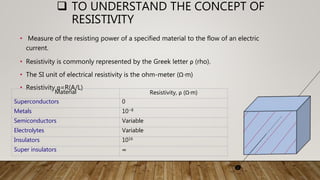
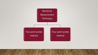
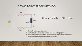
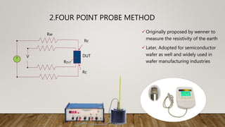
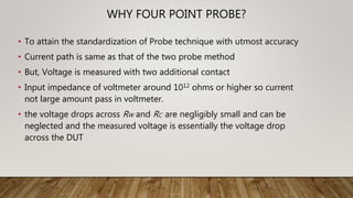
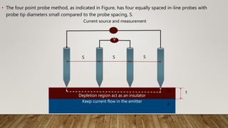
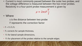
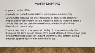
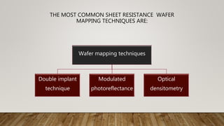
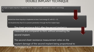
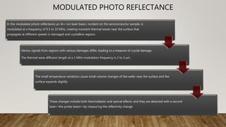
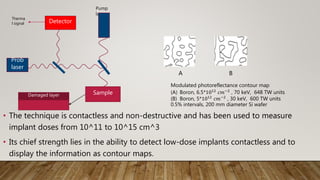
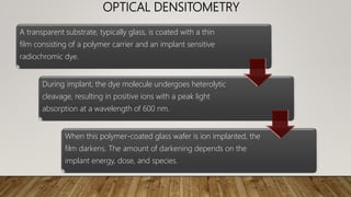
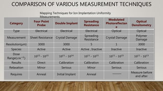
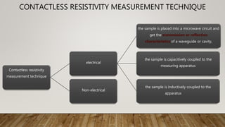
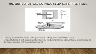
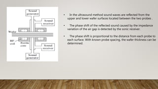
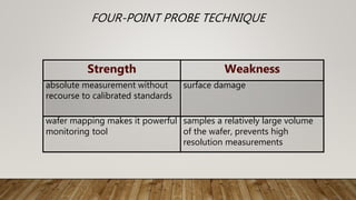
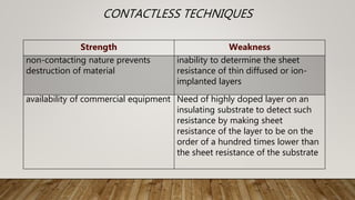
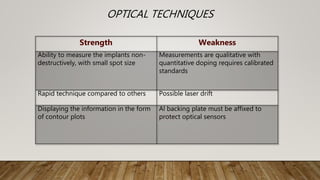
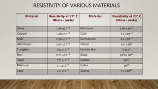
The document discusses techniques for measuring resistivity and mapping resistivity variations across semiconductor wafers. It begins by defining resistivity and listing typical resistivity values for different materials. It then describes two common measurement techniques: two-point probe and four-point probe. Four-point probe is more accurate as it eliminates lead and contact resistance. Factors that affect measurement accuracy like sample size, carrier injection, and probe spacing are also covered. The document concludes by explaining techniques for wafer mapping like double implant, modulated photoreflectance, and optical densitometry.
Threshold Voltage & Channel Length ModulationBulbul Brahma
Design and Technology of Electronic Devices:
Review of microelectronic devices, introduction to MOS technology and related devices.
MOS transistor theory, scaling theory related to MOS circuits, short channel effect and its
consequences, narrow width effect, FN tunnelling, Double gate MOSFET, Cylindrical
MOSFET, Basic concept of CMOS circuits and logic design. Circuit characterization and
performance estimation, important issues in real devices. PE logic, Domino logic, Pseudo
N-MOS logic-dynamic CMOS and Clocking, layout design and stick diagram, CMOS
analog circuit design, CMOS design methods. Introduction to SOI, Multi layer circuit
design and 3D integration. CMOS processing technology: Crystal grown and Epitaxy, Film
formation, Lithography and Etching, Impurity doping, Integrated Devices.
In MOS, source-drain regions of adjacent MOS transistors together with interconnection metal lines may constitute parasitic MOS transistors unless they are isolated from each other. Hence, each MOSFET must be electrically isolated from each other. Device Isolation Techniques in VLSI microfabrication of MOS are discussed.
Original Uni-junction transistor or UJT is a simple device in which a bar of N-type semiconductor material into which P-type material is diffused; somewhere along its length defining the device parameter as intrinsic standoff. The 2N2646 is the most commonly used version of UJT.
The three terminals of the FET are known as Gate, Drain, and Source.
It is a voltage controlled device, where the input voltage controls by the output current.
In FET current used to flow between the drain and the source terminal. And this current can be controlled by applying the voltage between the gate and the source terminal.
So this applied voltage generate the electric field within the device and by controlling these electric field we can control the flow of current through the device.
Here are the all short channel effects that you require.It consist of:-
Drain Induced Barrier Lowering
Hot electron Effect
Impact Ionization
Surface Scattering
Velocity saturation
Measurement is the estimation of the magnitude of some attribute of an object, such as its length or weight, relative to a unit of measurement.
Measurement usually involves using a measuring instrument, such as a ruler or scale, which is calibrated to compare the object to some standard, such as a meter or a kilogram. In science, however, where accurate measurement is crucial, a measurement is understood to have three parts: first, the measurement itself, second, the margin of error, and third, the confidence level -- that is, the probability that the actual property of the physical object is within the margin of error.
For example, we might measure the length of an object as 2.34 meters plus or minus 0.01 meter, with a 95% level of confidence.
At the applied voltage a disc-shaped cavity with partial discharges are measured at variable frequency (0.01-50 Hz). By varying the frequency it was observed that measured PD phase, magnitude of distributions and number of PDs per voltage cycles are varied. In the cavity, sequence of Partial discharge is simulated dynamically. For that purpose a model is presented with charge consistent. Simulated results shows that cavity surface and emission properties are effected by varying the magnitude of applied frequency, mainly conductivity of surface. This paper is illustrating the frequency dependence of PD in a cavity. The paper illustrates how the applied voltage amplitude and the cavity size can influence the frequency dependence PD activity.
Design of the Probe Sensor for the TDR Soil Moisture Sensor SystemIJLT EMAS
The probe sensor is of two parallel plates type which is used to determine the moisture content of the soil. The probe sensor is connected to a resistance to time period converter circuit of the TDR soil moisture sensor system whose output time period depends upon the resistance of the soil which in turn depends upon the moisture content of the soil acting as medium between the plates of the probe sensor. The TDR probe sensor is designed and simulated using the Integrated Electro software in order to determine the effects of the parameters like length, thickness and gap between the plates on electric field and energy density. The simulation results are used to predict and determine the geometry of the probe sensor, the materials that should be used in making the plates of the probe sensor and coating the plates of the probe sensor for reducing the effects of the fringing field and noise in the environment.
Scanning Probe microscopy (AFM and STM) head point
AFM: Configuration of AFM
Parts of AFM system and Principle of AFM
Three Modes of AFM
AFM Instrument
Advantage and disadvantage
STM
Schematic Diagram
AFM and STM
https://www.linkedin.com/in/preeti-choudhary-266414182/
https://www.instagram.com/chaudharypreeti1997/
https://www.facebook.com/profile.php?id=100013419194533
https://twitter.com/preetic27018281
Please like, share, comment and follow.
stay connected
If any query then contact:
chaudharypreeti1997@gmail.com
Thanking-You
Preeti Choudhary
To perform geological exploration by the geophysical method of electrical resistivity.
The objective of this research is to evaluate the water potential of the study area by
investigating the shallow subsurface aquifer material properties and moisture distribution using
2D ERT techniques. During the shallow tube well design and development in the study area,
some patches of land does have good potential and some does not, which motivated to
understand the aquifer properties, aquifer material, and response. Hence the 2D ERT was
carried out, oriented around the pond in the center and five ERT profiles.
Reference:IS 15736: 2007
To perform geological exploration by the geophysical method of electrical resistivity.
The objective of this research is to evaluate the water potential of the study area by investigating the shallow subsurface aquifer material properties and moisture distribution using 2D ERT techniques. During the shallow tube well design and development in the study area, some patches of land does have good potential and some does not, which motivated to understand the aquifer properties, aquifer material, and response. Hence the 2D ERT was carried out, oriented around the pond in the center and five ERT profiles.
The French Revolution, which began in 1789, was a period of radical social and political upheaval in France. It marked the decline of absolute monarchies, the rise of secular and democratic republics, and the eventual rise of Napoleon Bonaparte. This revolutionary period is crucial in understanding the transition from feudalism to modernity in Europe.
For more information, visit-www.vavaclasses.com
Synthetic Fiber Construction in lab .pptxPavel ( NSTU)
Synthetic fiber production is a fascinating and complex field that blends chemistry, engineering, and environmental science. By understanding these aspects, students can gain a comprehensive view of synthetic fiber production, its impact on society and the environment, and the potential for future innovations. Synthetic fibers play a crucial role in modern society, impacting various aspects of daily life, industry, and the environment. ynthetic fibers are integral to modern life, offering a range of benefits from cost-effectiveness and versatility to innovative applications and performance characteristics. While they pose environmental challenges, ongoing research and development aim to create more sustainable and eco-friendly alternatives. Understanding the importance of synthetic fibers helps in appreciating their role in the economy, industry, and daily life, while also emphasizing the need for sustainable practices and innovation.
The Roman Empire A Historical Colossus.pdfkaushalkr1407
The Roman Empire, a vast and enduring power, stands as one of history's most remarkable civilizations, leaving an indelible imprint on the world. It emerged from the Roman Republic, transitioning into an imperial powerhouse under the leadership of Augustus Caesar in 27 BCE. This transformation marked the beginning of an era defined by unprecedented territorial expansion, architectural marvels, and profound cultural influence.
The empire's roots lie in the city of Rome, founded, according to legend, by Romulus in 753 BCE. Over centuries, Rome evolved from a small settlement to a formidable republic, characterized by a complex political system with elected officials and checks on power. However, internal strife, class conflicts, and military ambitions paved the way for the end of the Republic. Julius Caesar’s dictatorship and subsequent assassination in 44 BCE created a power vacuum, leading to a civil war. Octavian, later Augustus, emerged victorious, heralding the Roman Empire’s birth.
Under Augustus, the empire experienced the Pax Romana, a 200-year period of relative peace and stability. Augustus reformed the military, established efficient administrative systems, and initiated grand construction projects. The empire's borders expanded, encompassing territories from Britain to Egypt and from Spain to the Euphrates. Roman legions, renowned for their discipline and engineering prowess, secured and maintained these vast territories, building roads, fortifications, and cities that facilitated control and integration.
The Roman Empire’s society was hierarchical, with a rigid class system. At the top were the patricians, wealthy elites who held significant political power. Below them were the plebeians, free citizens with limited political influence, and the vast numbers of slaves who formed the backbone of the economy. The family unit was central, governed by the paterfamilias, the male head who held absolute authority.
Culturally, the Romans were eclectic, absorbing and adapting elements from the civilizations they encountered, particularly the Greeks. Roman art, literature, and philosophy reflected this synthesis, creating a rich cultural tapestry. Latin, the Roman language, became the lingua franca of the Western world, influencing numerous modern languages.
Roman architecture and engineering achievements were monumental. They perfected the arch, vault, and dome, constructing enduring structures like the Colosseum, Pantheon, and aqueducts. These engineering marvels not only showcased Roman ingenuity but also served practical purposes, from public entertainment to water supply.
2024.06.01 Introducing a competency framework for languag learning materials ...Sandy Millin
http://sandymillin.wordpress.com/iateflwebinar2024
Published classroom materials form the basis of syllabuses, drive teacher professional development, and have a potentially huge influence on learners, teachers and education systems. All teachers also create their own materials, whether a few sentences on a blackboard, a highly-structured fully-realised online course, or anything in between. Despite this, the knowledge and skills needed to create effective language learning materials are rarely part of teacher training, and are mostly learnt by trial and error.
Knowledge and skills frameworks, generally called competency frameworks, for ELT teachers, trainers and managers have existed for a few years now. However, until I created one for my MA dissertation, there wasn’t one drawing together what we need to know and do to be able to effectively produce language learning materials.
This webinar will introduce you to my framework, highlighting the key competencies I identified from my research. It will also show how anybody involved in language teaching (any language, not just English!), teacher training, managing schools or developing language learning materials can benefit from using the framework.
Biological screening of herbal drugs: Introduction and Need for
Phyto-Pharmacological Screening, New Strategies for evaluating
Natural Products, In vitro evaluation techniques for Antioxidants, Antimicrobial and Anticancer drugs. In vivo evaluation techniques
for Anti-inflammatory, Antiulcer, Anticancer, Wound healing, Antidiabetic, Hepatoprotective, Cardio protective, Diuretics and
Antifertility, Toxicity studies as per OECD guidelines
How to Make a Field invisible in Odoo 17Celine George
It is possible to hide or invisible some fields in odoo. Commonly using “invisible” attribute in the field definition to invisible the fields. This slide will show how to make a field invisible in odoo 17.
Francesca Gottschalk - How can education support child empowerment.pptxEduSkills OECD
Francesca Gottschalk from the OECD’s Centre for Educational Research and Innovation presents at the Ask an Expert Webinar: How can education support child empowerment?
Instructions for Submissions thorugh G- Classroom.pptxJheel Barad
This presentation provides a briefing on how to upload submissions and documents in Google Classroom. It was prepared as part of an orientation for new Sainik School in-service teacher trainees. As a training officer, my goal is to ensure that you are comfortable and proficient with this essential tool for managing assignments and fostering student engagement.
Unit 8 - Information and Communication Technology (Paper I).pdfThiyagu K
This slides describes the basic concepts of ICT, basics of Email, Emerging Technology and Digital Initiatives in Education. This presentations aligns with the UGC Paper I syllabus.
Introduction to AI for Nonprofits with Tapp NetworkTechSoup
Dive into the world of AI! Experts Jon Hill and Tareq Monaur will guide you through AI's role in enhancing nonprofit websites and basic marketing strategies, making it easy to understand and apply.
2. OUTLINE
• To understand the concept of resistivity
• Resistivity measurement technique
• Sheet resistance
• Measurement Errors and precautions
• Wafer Mapping
• Contactless resistivity measurement technique
• Strength and weaknesses of Various measurement
techniques
• Conclusion
3. TO UNDERSTAND THE CONCEPT OF
RESISTIVITY
• Measure of the resisting power of a specified material to the flow of an electric
current.
• Resistivity is commonly represented by the Greek letter ρ (rho).
• The SI unit of electrical resistivity is the ohm-meter (Ω⋅m)
• Resistivity ρ=R(A/L)
Material Resistivity, ρ (Ω·m)
Superconductors 0
Metals 10−8
Semiconductors Variable
Electrolytes Variable
Insulators 1016
Super insulators ∞
5. 1.TWO POINT PROBE METHOD
Basically a two point contact
Each contact serves as a current and as a voltage probe
Appear to be easier but the interpretation of the measured data is
difficult due to various resistance inclusion
Rw
V
Rw
Rc
Rc
RDUT
DUT
RT = V/I= 2RW + 2RC + RDUT
6. 2.FOUR POINT PROBE METHOD
Originally proposed by wenner to
measure the resistivity of the earth
Later, Adopted for semiconductor
wafer as well and widely used in
wafer manufacturing industries
V
Rw
Rc
Rc
RDUT
DUT
7. WHY FOUR POINT PROBE?
• To attain the standardization of Probe technique with utmost accuracy
• Current path is same as that of the two probe method
• But, Voltage is measured with two additional contact
• Input impedance of voltmeter around 1012 ohms or higher so current
not large amount pass in voltmeter.
• the voltage drops across RW and RC are negligibly small and can be
neglected and the measured voltage is essentially the voltage drop
across the DUT
8. • The four point probe method, as indicated in Figure, has four equally spaced in-line probes with
probe tip diameters small compared to the probe spacing, S.
Depletion region act as an insulator
Keep current flow in the emitter
V
N
P
t
S S S
Current source and measurement
9. • Current is most commonly passed between the outer two probes, and
the voltage difference is measured between the two inner probes.
Resistivity in a four-point probe measurement is given by
𝜌 = 2𝜋𝑠𝐹
𝑉
𝐼
• Where
s is the distance between two probe
F represents the correction factor
• F = F1 F2 F3
• F1 corrects for sample thickness,
• F2 for lateral sample dimensions,
• F3 for placement of the probes relative to the sample edges.
10. EXPERIMENTAL PROCEDURE:
Source.: F.M.Smits, "Measurement of Sheet Resistivities with the Four-Point Probe", The Bell System
Technical Journal 37, 711-718
Reference: RESISTIVITY OF A SEMICONDUCTOR BY THE FOUR-PROBE METHOD (Dr Jeethendra Kumar P K)
Let a Sample n-type Germanium Semiconductor
Dimensions : (L) 2mm x (d) 5.4mm x (t) 0.5mm
Probe Spacing (S) : 2mm
Resistivity for equally spaced probes is given
by
𝜌 = 2𝜋𝑠𝐹
𝑉
𝐼
Calculating ratios “t/S” and “d/S”
t/S = 0.25 ; d/S = 2.7
𝜌 = 4.53𝑡 × 𝐹 ×
𝑉
𝐼
It is observed by experimentation that the sample with thickness-gap
ratio t/S≤0.5, the geometric factor 2πS is given by
2πS =
𝜋
𝑙𝑛2
× 𝑡 =4.53t
Hence for a finite width and non-negligible thickness is
given by:
𝐹 = 𝑓1 𝑓2
Where 𝑓1 & 𝑓2 are determined from the graph
𝑓1 = 1 ; 𝑓2 = 0.59
𝜌 = 1.33 × 10⁻³ ×
𝑉
𝐼
11. The sample is placed under the four probes such that the probes are
parallel to the longer side (length) of the sample.
Reference: RESISTIVITY OF A SEMICONDUCTOR BY THE FOUR-PROBE METHOD (Dr Jeethendra Kumar P K)
The current is set to 0.1mA by adjusting set-current knob. The voltage
developed across the inner probes is noted
Current (mA)
Sample-1
mV V/I
0.1 5.4 54.0
0.2 10.5 52.5
0.3 16.0 53.3
0.4 21.1 52.7
0.5 26.5 53.0
0.6 31.7 52.8
0.7 37.0 52.8
0.8 42.3 53.3
0.9 48.0 53.0
1.0 53.0 53.0
1.1 58.3 53.0
1.2 63.5 52.9
1.3 69.0 53.0
1.4 74.4 53.1
1.5 79.8 53.2
Average V/I 53.0
𝜌 = 1.33 × 10−3
× 53
= 0.0708 𝛺 − 𝑚
= 7.08 𝛺 − 𝑐𝑚
12. SHEET RESISTANCE
• Measure of the resistivity averaged over the
surface
• Sheet resistance is a measure of resistance of
thin films that are nominally uniform in
thickness.
• The utility of sheet resistance as opposed
to resistance or resistivity is that it is directly
measured using a four-point probe
measurement or indirectly by using a non-
contact eddy current based testing device.
• Sheet resistance can be used to compare the
electrical properties of devices that are
significantly different in size.
𝑅 = 𝑅 𝑠ℎ
𝐿
𝑊
ohms
𝑅 = 𝜌
𝐿
𝐴
= 𝜌
𝐿
𝑊𝑡
=
𝜌
𝑡
𝐿
𝑊
Ohms
13. CONTD.
• Since
𝐿
𝑊
has no units,
𝜌
𝑡
should have units of ohms. But
𝜌
𝑡
is not the sample
resistance.
• To distinguish between R and
𝜌
𝑡
, Often in practice, surface resistivity is given in
units of
Ω
𝑆𝑞𝑢𝑎𝑟𝑒
• Sheet resistance is applicable as long as the measurement is related to a square.
14. Minority Majority
(carrier injection)
Probe spacing
CurrentSample Size
High Resistivity
Materials
FACTORS AFFECTING THE MEASUREMENT ACCURACY
Measurement
Errors and
Precautions
15. SAMPLE SIZE
• correction factor F depends on the thickness of the material
• If the wafer or the layer to be measured is appreciably thinner than the probe spacing,
the calculated resistivity varies directly with thickness.
• It is therefore very important to determine the thickness accurately for resistivity
determination.
16. MINORITY - MAJORITY CARRIER INJECTION
• Metal-semiconductor contacts do inject minority carriers, but their injection efficiency is
low.
• However, under high current conditions it may not be negligible.
• Minority carrier injection causes conductivity modulation because increased minority
carrier density leads to increased majority carrier density (to maintain charge neutrality)
and subsequent enhanced conductivity.
• To reduce minority carrier injection, the surface should have a high recombination rate for
minority carriers. This is best achieved by using lapped surfaces.
17. PROBE SPACING
• A mechanical four-point probe exhibits small random probe spacing
variations.
• Such variations give erroneous values of resistivity or sheet resistance,
especially when evaluating uniformly doped wafers.
• In such cases it is very important to know whether any non-uniformities are
due to the wafer, due to process variations, or due to measurement errors.
18. CURRENT
• The current can affect the
measured resistivity in two ways:
1. by an apparent resistivity increase
produced by wafer heating
2. by an apparent resistivity
decrease due to minority and/or
majority carrier injection.
10−2
10−1
100
101
102
103
10−2
10−1
100
101
102
103
104
Current (mA)
Resistivity(Ω-cm)
SheetResistance(Ω-
Square)
19. HIGH RESISTIVITY MATERIALS
• Materials of very high resistivity are more difficult to measure by four-point probe method.
• Moderately doped wafers can become highly resistive at low temperatures and are similarly
difficult to measure.
20. WAFER MAPPING
• originated in the 1970s
• originally developed to characterize ion implantation uniformity
• During wafer mapping the sheet resistance or some other parameter
proportional to ion implant dose is measured at many locations across a
sample. The data are then converted to two-dimensional or three-
dimensional contour maps
• Contour maps are a more powerful display of process uniformity than
displaying the same data in tabular form. A well-designed contour map gives
instant information about ion implant uniformity, flow patterns during
diffusion, epitaxial reactor non-uniformities, etc.
21. THE MOST COMMON SHEET RESISTANCE WAFER
MAPPING TECHNIQUES ARE:
Wafer mapping techniques
Double implant
technique
Modulated
photoreflectance
Optical
densitometry
22. DOUBLE IMPLANT TECHNIQUE
A p-type (n-type) impurity is implanted into an n-type (p-type) substrate at a dose 1 and energy
E1.
desired low-dose impurity is implanted at dose 2 and energy E2, with E2 < E1.
E2 should be less than E1 to prevent penetration through the first implant layer.
The sheet resistance Rsh2 after the second implant is
measured and compared to Rsh1 without annealing the
second implant.
The second sheet resistance measurement relies on the
implant damage of the second implant being proportional to
the implant dose.
23. Four-point probe sheet resistance
Four- point prob contour map
(A) Boron, 1015
𝑐𝑚−2
, 40 keV, Rsh (average) = 98.5 ohms/square
(B) (B) Arsenic, 1015 𝑐𝑚−2 , 80 keV, Rsh (average) = 98.5 ohms/square
1% intervals, 200 mm diameter Si wafer
A B
24. MODULATED PHOTO REFLECTANCE
In the modulated photo reflectance ,an Ar+ ion laser beam, incident on the semiconductor sample, is
modulated at a frequency of 0.1 to 10 MHz, creating transient thermal waves near the surface that
propagate at different speeds in damaged and crystalline regions.
Hence, signals from regions with various damages differ, leading to a measure of crystal damage.
The thermal wave diffusion length at a 1 MHz modulation frequency is 2 to 3 μm.
The small temperature variations cause small volume changes of the wafer near the surface and the
surface expands slightly.
These changes include both thermoelastic and optical effects, and they are detected with a second
laser—the probe beam—by measuring the reflectivity change
25. • The technique is contactless and non-destructive and has been used to measure
implant doses from 10^11 to 10^15 cm^3
• Its chief strength lies in the ability to detect low-dose implants contactless and to
display the information as contour maps.
Damaged layer
Therma
l signal
Pump
laser
Sample
Detector
Prob
laser
Modulated photoreflectance contour map
(A) Boron, 6.5*1012
𝑐𝑚−2
, 70 keV, 648 TW units
(B) Boron, 5*1012
𝑐𝑚−2
, 30 keV, 600 TW units
0.5% intervals, 200 mm diameter Si wafer
A B
26. OPTICAL DENSITOMETRY
A transparent substrate, typically glass, is coated with a thin
film consisting of a polymer carrier and an implant sensitive
radiochromic dye.
During implant, the dye molecule undergoes heterolytic
cleavage, resulting in positive ions with a peak light
absorption at a wavelength of 600 nm.
When this polymer-coated glass wafer is ion implanted, the
film darkens. The amount of darkening depends on the
implant energy, dose, and species.
27. COMPARISON OF VARIOUS MEASUREMENT TECHNIQUES
Category
Four Point
Probe
Double Implant
Spreading
Resistance
Modulated
Photoreflectan
e
Optical
Densitometry
Type Electrical Electrical Electrical Optical Optical
Measurement Sheet Resistance Crystal Damage
Spreading
Resistance
Crystal Damage
Polymer
Damage
Resolution(µm) 3000 3000 5 1 3000
Species Active Active Active , Inactive Inactive Inactive
Dose
Range(𝑐𝑚−2
)
1012 - 1015 1011 - 1014
1011 - 1015 1011 - 1015 1011 - 1013
Results Direct Calibration Calibration Calibration Calibration
Relaxation Minor Serious Minor Serious Serious
Requires Anneal Initial Implant Anneal
_______ Measure before
and after
Mapping Techniques for Ion Implantation Uniformity
Measurements
28. CONTACTLESS RESISTIVITY MEASUREMENT TECHNIQUE
Contactless resistivity
measurement technique
electrical
the sample is placed into a microwave circuit and
get the transmission or reflection
characteristics of a waveguide or cavity,
the sample is capacitively coupled to the
measuring apparatus
the sample is inductively coupled to the
apparatus
Non-electrical
29. ONE SUCH CONTACTLESS TECHNIQUE IS EDDY CURRENT TECHNIQUE
• The eddy current measurement technique is based on the parallel resonant tank circuit.
• The quality factor of such a circuit is reduced when a conducting material is brought close to the coil due to
the power absorbed by the conducting material.
30. • In the ultrasound method sound waves are reflected from the
upper and lower wafer surfaces located between the two probes .
• The phase shift of the reflected sound caused by the impedance
variation of the air gap is detected by the sonic receiver.
• The phase shift is proportional to the distance from each probe to
each surface. With known probe spacing, the wafer thickness can be
determined.
32. FOUR-POINT PROBE TECHNIQUE
Strength Weakness
absolute measurement without
recourse to calibrated standards
surface damage
wafer mapping makes it powerful
monitoring tool
samples a relatively large volume
of the wafer, prevents high
resolution measurements
33. CONTACTLESS TECHNIQUES
Strength Weakness
non-contacting nature prevents
destruction of material
inability to determine the sheet
resistance of thin diffused or ion-
implanted layers
availability of commercial equipment Need of highly doped layer on an
insulating substrate to detect such
resistance by making sheet
resistance of the layer to be on the
order of a hundred times lower than
the sheet resistance of the substrate
34. OPTICAL TECHNIQUES
Strength Weakness
Ability to measure the implants non-
destructively, with small spot size
Measurements are qualitative with
quantitative doping requires calibrated
standards
Rapid technique compared to others Possible laser drift
Displaying the information in the form
of contour plots
Al backing plate must be affixed to
protect optical sensors
35. EFFECT OF PRESSURE ON RESISTIVITY OF
SEMICONDUCTORS:
Amorphous Silicon
• Effects of hydrostatic pressure on
electrical resistively of Amorphous
Silicon at room temperature have been
experimentally investigated and
plotted in the graph as shown
36. Selenium
• Selenium is other group material with a direct band gap in
type conduction. It is used in selenium rectifiers.
• The effects of pressure on the optical edge of selenium have
been studied by Balchan and Drickamer
GermaniumSelenium
37. RESISTIVITY OF VARIOUS MATERIALS
Material Resistivity at 23º C
Ohms - meter
Material Resistivity at 23º C
Ohms - meter
Silver 1.59 𝑥10−8 Nichrome 1.50 𝑥10−6
Copper 1.68 𝑥10−8 Coal 3.5 𝑥10−5
Gold 2.20 𝑥10−8 Germanium 4.6 𝑥10−1
Aluminum 2.65 𝑥10−8 Silicon 6.4 𝑥102
Tungsten 5.6 𝑥10−8 Human Skin 5 𝑥105
Iron 9.71 𝑥10−8 Glass 101
𝑡𝑜 1014
Steel 7.2 𝑥10−7 Rubber 1013
Platinum 1.1 𝑥10−7 Sulfur 1015
Lead 2.2 𝑥10−7 Quartz 7.5 𝑥1017
38. • Reference:
1. Semiconductor Material And Device Characterization By Dieter K.
Schroder
2. Electrical resistivity/ resistance of some semiconductors by Rajendra
Kumar and Tanveer Ahmad Wani