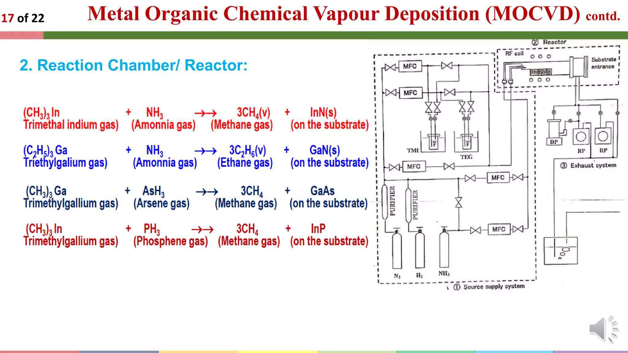
Have an overview of the most conventionally utilized crystal growth techniques: process, diagrams, advantages, and disadvantages. This is the presentation of my "PV cells and materials" course at the MSc Engg. level.
Epitaxial deposition is a method for growing high quality crystalline films on crystalline substrates. There are two main types: homoepitaxy, where the film and substrate are the same material, and heteroepitaxy, where they differ. Key parameters that affect the epitaxial growth process include temperature, pressure, and reactant flow. Common techniques include vapor phase epitaxy, liquid phase epitaxy, and molecular beam epitaxy, each with their own advantages and disadvantages for producing films for semiconductor and optoelectronic devices.
Molecular beam epitaxy (MBE) is a method for growing thin films one layer at a time under ultra-high vacuum conditions. It involves heating solid sources of material in effusion cells to create molecular beams that are deposited on a heated substrate. The absence of carrier gases and ultra-high vacuum environment result in films of the highest purity. MBE is widely used to manufacture semiconductor devices and is considered a fundamental tool for nanotechnology development due to its precise control over layer thickness down to a single atomic layer.
If you have any questions, contact me. I would be happy to help.
PLEASE LIKE IT AND GIVE COMMENT
In this presentation,
The author gives the working principle of the PVD and Sputtering methods. But you can also find an information about the thin film and plasma phase of a matter.
Also this is related with Magnetron Sputtering method.
Electron beam lithography uses a focused beam of electrons to directly write nanoscale patterns onto a resist-coated surface. It allows for very high resolution patterning down to a few nanometers in size. The process involves coating a surface with an electron-sensitive resist, using a focused electron beam to expose patterns in the resist according to design data, and then developing the resist to selectively remove the exposed or unexposed areas. Key advantages of electron beam lithography include its lack of diffraction limit on resolution and ability to create specialized device structures. However, it also has disadvantages like long write times and high system costs.
Ic technology- chemical vapour deposition and epitaxial layer growthkriticka sharma
This document discusses chemical vapor deposition (CVD) and epitaxial layer growth techniques used in integrated circuit technology. It begins with an overview of CVD, describing the basic process and steps involved, including transport of reactants, adsorption, surface reactions, and removal of byproducts. It then covers various types of CVD systems like atmospheric pressure CVD, low pressure CVD, and plasma-enhanced CVD. The document also discusses epitaxial growth techniques like vapor phase epitaxy and molecular beam epitaxy. It explains concepts like lattice matching and defects that can occur during heteroepitaxial growth when the film and substrate materials have different lattice constants.
This document provides an overview of thin film deposition methods and thin film characterization techniques. It discusses the objectives of the course, which are to provide an understanding of thin film deposition methods, their capabilities and limitations. Hands-on demonstrations and experiments will help participants understand each deposition method and stimulate discussion. The document then summarizes various thin film deposition techniques like evaporation, sputtering, chemical vapor deposition, their principles and examples of applications. It also summarizes various characterization techniques used to analyze thin films and determine properties like composition, structure, thickness and defects.
This document provides information on preparing thin films using the Successive Ionic Layer Adsorption and Reaction (SILAR) method. It discusses what thin films are, common thin film deposition techniques like physical vapor deposition and chemical vapor deposition, and the SILAR method specifically. SILAR involves alternating immersion of a substrate in cationic and anionic precursor solutions to deposit materials like cadmium sulfide in a layer-by-layer process. Parameters like concentration, pH, temperature, and deposition time must be optimized to produce adherent thin films. The document also outlines some applications of SILAR-deposited cadmium sulfide thin films and factors that influence thin film characteristics.
This document discusses thin film applications such as solar cells, thin film transistors, optical coatings, and thin film batteries. It provides details on how each of these applications uses thin films, including how solar cells convert light to electricity using electron-hole pairs, how thin film transistors act as switches in LCD displays, and how optical coatings can reduce reflections. Thin film batteries are also summarized as being solid-state and potentially flexible. In general, the document outlines the key uses and operating principles of several important thin film technologies.
Lithography is a process that uses light to transfer geometric patterns from a photomask to a light-sensitive chemical "photoresist" on a semiconductor substrate. The key steps in the lithography process include cleaning and preparing the wafer surface, depositing and spinning photoresist, soft baking to evaporate solvents, aligning the mask and exposing the photoresist to light, developing to remove exposed or unexposed areas of photoresist, hard baking to harden the photoresist, plasma etching or depositing additional layers, cleaning, and inspecting the final patterned wafer. Lithography is critical for manufacturing integrated circuits and is capable of printing ever smaller semiconductor features.
Molecular beam epitaxy (MBE) is a technique for growing crystalline thin films one atomic layer at a time by heating a substrate and directing beams of molecules or atoms onto the substrate from various solid sources placed in evaporation cells. The technique allows for precise and pure layering of compound semiconductor materials less than 0.01 nanometers thick. MBE is used to produce complex semiconductor structures that can then be processed into electronic and optoelectronic devices like transistors, light-emitting diodes, solar cells, and lasers used in applications such as fiber optics, phones, satellites, and displays.
Thin film deposition using spray pyrolysisMUHAMMAD AADIL
Spray pyrolysis is a simple and low-cost thin film deposition technique that involves spraying a metal salt solution onto a heated substrate. As the droplets impact and spread on the substrate, thermal decomposition occurs, leaving a film of metal oxides. The substrate temperature is the main parameter that determines the film properties, as it influences processes like precursor decomposition and solvent evaporation. Varying the deposition temperature can control the film morphology and optical/electrical characteristics. The precursor solution composition also affects the film structure, as additives can modify the solution chemistry and change the resulting film morphology.
Physical vapor deposition (PVD) involves evaporating or sputtering material in vacuum chambers to form thin films or coatings on surfaces. Different PVD techniques include evaporative deposition using resistive heating or electron beams, sputter deposition using plasma or ion beams, and pulsed laser deposition. PVD is commonly used for circuit fabrication, aerospace coatings, and optics due to its ability to deposit thin, uniform coatings of various materials at high temperatures and precise thicknesses. Some advantages of PVD include producing environmentally friendly coatings without requiring post-deposition treatments, while disadvantages include high energy and vacuum requirements.
This document discusses electron beam lithography. It begins with an introduction and overview of electron beam lithography, explaining that it uses a beam of electrons to selectively expose and develop a resist film in order to create very small structures. It then provides a schematic of the electron beam lithography process and describes the lithography process steps. The document also covers the advantages of high resolution and no diffraction limit but disadvantages of low throughput and high costs. It includes details on electron beam sources and lenses used.
ALD is a thin film deposition technique based on self-terminating surface reactions of gas precursors. It involves alternating exposure of a substrate to different precursors separated by purge steps, resulting in one atomic layer of film growth per cycle. ALD provides highly conformal and uniform coatings with atomic-level thickness control due to its self-limiting growth mechanism. It is widely used for depositing oxides, nitrides and some metals in applications such as semiconductors, coatings, MEMS and solar cells.
Electron beam lithography (often abbreviated as e-beam lithography or EBL) is the process of transferring a pattern onto the surface of a substrate by first scanning a thin layer of organic film (called resist) on the surface by a tightly focused and precisely controlled electron beam (exposure) and then selectively removing the exposed or nonexposed regions of the resist in a solvent (developing). The process allows patterning of very small features, often with the dimensions of submicrometer down to a few nanometers, either covering the selected areas of the surface by the resist or exposing otherwise resist-covered areas. The exposed areas could be further processed for etching or thin-film deposition while the covered parts are protected during these processes. The advantage of e-beam lithography stems from the shorter wavelength of accelerated electrons compared to the wavelength of ultraviolet (UV) light used in photolithography.
In EBL, a resist layer is directly patterned by scanning with an electron beam electronically. Modern EBL systems have very good depth of focus (several hundred nanometres) and are able to correct for large-scale height variations of the wafer (of several hundred microns), and so are able to cope well with the rough surface topology of typical GaN wafers and associated wafer bow. EBL also has the advantage of allowing multiple designs to be fabricated together on one wafer. EBL is, however, a slow and expensive process, which is not practical for production. Substrate charging and proximity error effects must be taken into account to get good quality devices. Charging effects can be overcome by application of a sub-nanoscale removable conductive layer on top of the resist. Proximity error correction effects are overcome using specialised design correction software.
Metal Organic Chemical Vapour Deposition (MOCVD) is a technique used to grow thin semiconductor films on substrates using organometallic compounds as sources. MOCVD is commonly used to fabricate electronic and optoelectronic devices like those in phones, LEDs, and solar cells. The MOCVD process involves heating substrates in a reactor where organometallic source gases decompose and react to form epitaxial semiconductor films precisely controlled in thickness and composition. MOCVD offers high growth quality, flexibility, and throughput making it well-suited for heterostructures like quantum wells used across many applications.
Physical vapor deposition (PVD) is a process that deposits thin films of material onto a substrate through the physical vaporization of source material and subsequent condensation. There are two main PVD techniques - thermal evaporation and sputtering. Thermal evaporation uses resistive heating to vaporize the source material in a vacuum, while sputtering uses plasma to bombard the source material and eject atoms through momentum transfer. PVD is used to deposit films ranging from nanometers to micrometers thick for applications such as decorative coatings, electronic devices, and wear-resistant tool coatings.
This document discusses epitaxial crystal growth from vapor phase. Epitaxial growth involves depositing a mono-crystalline film onto a mono-crystalline substrate, allowing the deposited film to take on the same ordered lattice structure and orientation. There are two main types of epitaxial films: homoepitaxy, where the deposited layer is of the same material as the substrate, and heteroepitaxy, where the deposited layer is of a different material. Epitaxial growth is useful for applications requiring high purity, low defect density, and controlled doping profiles. Vapor phase epitaxy is a common deposition method and epitaxial layers find applications in nanotechnology, semiconductor fabrication, and high quality crystal growth.
Photolithography, also called optical lithography or UV lithography, is a process used in microfabrication to pattern parts on a thin film or the bulk of a substrate (also called a wafer). It uses light to transfer a geometric pattern from a photomask (also called an optical mask) to a photosensitive (that is, light-sensitive) chemical photoresist on the substrate. A series of chemical treatments then either etches the exposure pattern into the material or enables deposition of a new material in the desired pattern upon the material underneath the photoresist. In complex integrated circuits, a CMOS wafer may go through the photolithographic cycle as many as 50 times.
Photolithography shares some fundamental principles with photography in that the pattern in the photoresist etching is created by exposing it to light, either directly (without using a mask) or with a projected image using a photomask. This procedure is comparable to a high precision version of the method used to make printed circuit boards. Subsequent stages in the process have more in common with etching than with lithographic printing. This method can create extremely small patterns, down to a few tens of nanometers in size. It provides precise control of the shape and size of the objects it creates and can create patterns over an entire surface cost-effectively. Its main disadvantages are that it requires a flat substrate to start with, it is not very effective at creating shapes that are not flat, and it can require extremely clean operating conditions. Photolithography is the standard method of printed circuit board (PCB) and microprocessor fabrication. Directed self-assembly is being evaluated as an alternative to photolithography
The document describes the key steps in the semiconductor manufacturing process including silicon manufacturing using the Czochralski method, photolithography using photoresists and photomasks, and ion implantation. Photolithography involves coating wafers with photoresist, exposing it to light through a photomask, and developing the resist to transfer patterns. Ion implantation injects dopants by accelerating ions toward the wafer surface.
Photolithography uses ultraviolet light to etch designs onto silicon wafers coated with photoresist. There are two types of lithography used to make microfluidic chips: photolithography and soft lithography. Photolithography involves using UV light to create molds on silicon wafers, while soft lithography uses those molds to make chips from PDMS polymer. The photolithography process involves priming, coating, exposing, and developing the wafer using a photomask to transfer the desired pattern to the photoresist. There are two types of photoresist - positive and negative - which determine whether the exposed or unexposed areas are removed during development.
Physical and chemical vapor deposition.pptxMMuslimRehman
This document discusses various thin film deposition techniques, including physical vapor deposition (PVD) and chemical vapor deposition (CVD). It describes how PVD techniques like evaporation and sputtering use thermal or ion beam methods to remove growth species from a source and deposit them on a substrate. Molecular beam epitaxy is noted as a precise PVD method. CVD involves chemical reactions of volatile precursors on a heated substrate, producing a deposited film and gaseous byproducts. The kinetics and types of CVD reactors are also summarized.
- Epitaxy involves the deposition and growth of crystalline layers on a substrate in a way that matches the substrate's crystalline structure. This results in single-crystal layers.
- Common epitaxy techniques discussed are vapor-phase epitaxy (VPE), liquid-phase epitaxy (LPE), and molecular beam epitaxy (MBE).
- MBE involves evaporating source materials in an ultra-high vacuum and allowing them to condense on a heated substrate. It allows precise control over composition and doping at the monolayer level.
1. Chemical vapor deposition (CVD) is a common bottom-up nanomaterial synthesis method that involves decomposing a gaseous precursor on a substrate. The presence of a catalyst activates the chemical reaction between the substrate surface and precursor.
2. Plasma-enhanced CVD (PECVD) is preferred over thermal CVD because it allows lower process temperatures and more directional nanomaterial growth using plasma fields.
3. Common CVD methods for producing carbon nanotubes include thermal CVD where a carbon source like acetylene decomposes on a metal catalyst particle at high temperatures, guiding nanotube growth.
This document discusses molecular beam epitaxy (MBE), a process for depositing thin crystalline films. MBE involves heating pure elements in separate cells under high vacuum and allowing them to condense as a film on a substrate. It allows precise control over film thickness and composition to grow structures like semiconductor lasers. In-situ diagnostics like reflection high-energy electron diffraction (RHEED) are used to monitor growth. Challenges include the Ataro-Tiller-Grinfeld instability that can cause cracking in the film above a critical thickness if the substrate and film have a lattice mismatch.
This document provides an overview of molecular beam epitaxy (MBE) for thin film deposition. MBE involves heating pure elements in separate cells and evaporating them as molecular beams in ultra-high vacuum onto a substrate. This allows for layer-by-layer crystal growth at slow deposition rates. Key aspects of MBE include the use of shutters and in-situ diagnostics to control layer thickness and monitor crystal quality. Challenges include stresses that can cause cracking in films with large lattice mismatches to the substrate.
This document provides information on various thin film deposition techniques used in nano electronics, including physical vapor deposition (PVD) methods like evaporation, sputtering, and ion plating. It also discusses chemical vapor deposition (CVD) and its types like atmospheric pressure CVD, low-pressure CVD, plasma-enhanced CVD, as well as epitaxy and molecular beam epitaxy (MBE). Other topics covered include ion implantation equipment and process, radiation damage from implantation, and formation of silicon oxide through thermal oxidation.
Bottom up approaches for nanoparticle synthesiskusumDabodiya
The document discusses bottom-up approaches for synthesizing nanomaterials. Bottom-up approaches involve building nanostructures from individual atoms and molecules, as opposed to top-down approaches which break down bulk materials. Some key bottom-up techniques described are physical vapor deposition methods like inert gas condensation, thermal evaporation, sputtering, and laser ablation which use gas precursors. Liquid phase bottom-up methods including wet chemical synthesis and microemulsion techniques are also covered. The document provides details on the mechanisms and advantages of various bottom-up synthesis methods.
This document provides information about molecular beam epitaxy (MBE) for thin film growth. MBE uses beams of molecules in an ultra-high vacuum to deposit thin crystalline films one layer at a time onto a substrate. Key aspects of MBE include its very low deposition rate, the use of shutters to control layer thickness at an atomic level, and in-situ monitoring using reflection high-energy electron diffraction. Challenges include the Ataro-Tiller-Grinfeld instability that can cause films to crack due to lattice mismatch with the substrate.
Molecular Beam Epitaxy (MBE) is a technique used to grow thin crystalline films one layer at a time under ultra-high vacuum conditions. In MBE, beams of molecules or atoms are directed towards a heated crystalline substrate where they condense in an ordered manner. This allows precise control over composition at the atomic or molecular level. MBE provides highly pure and flexible epitaxial growth for applications such as transistors, microwave and optoelectronic devices using materials like III-V semiconductors. While offering clean and well-controlled results, MBE also has high equipment costs and long setup times.
Epitaxial growth involves depositing a crystalline film on a crystalline substrate in an ordered manner. There are two main types: homoepitaxy, where the film and substrate are the same material, and heteroepitaxy, where they are different. Molecular beam epitaxy (MBE) is a technique that grows thin films one atomic layer at a time in an ultra-high vacuum environment using beams of molecules or atoms from effusion cells that are deposited on a heated substrate. MBE allows for precise control over composition and thickness at the atomic scale and is used to produce high-quality semiconductors and quantum structures for applications in nanotechnology, optoelectronics, and more.
Bioceramic dental implant coatings (Deposited and converted coatings ).
This presentation discusses the different techniques used to coat dental implants to enhance osseointegration .
Chemical Vapour Deposition is a Chemical Synthesis route of Nanomaterials. Specially thin films like Graphene and Carbon NanoTubes are grown by this method.
Hot wall reactor is a high temperature chamber in which the substrate is placed for coating. In this reactor including the substrate, all other parts (inlet and outlet tubes) inside the chamber get coated.
The document discusses nanomaterial synthesis methods. It begins with an introduction to nanotechnology and challenges in the field. It then covers bottom-up and top-down approaches to nanomaterial synthesis. Specific synthesis methods covered include evaporation and condensation growth, lithography technology, and methods for creating nano-composites. A variety of nanoparticle synthesis techniques are also discussed.
The document discusses thin film deposition techniques used in semiconductor manufacturing. It covers physical vapor deposition (PVD) methods like evaporation and sputtering as well as chemical vapor deposition (CVD). Evaporation involves heating a source material to produce a vapor that deposits on wafers in a vacuum chamber. Sputtering uses argon plasma to eject atoms from a target material that then deposit on wafers. CVD techniques like APCVD and LPCVD use chemical reactions or decomposition of precursor gases to deposit thin films. The document discusses parameters, characteristics and challenges of thin film deposition methods.
Nanotechnology refers to manipulating atoms and structures at the nanoscale (1-100 nm) to design and produce novel materials. Nanoscience studies unique properties of nanomaterials, while nanotechnology applies this research. Nanomaterials have unique optical, electrical, or magnetic properties at the nanoscale that can be utilized in fields like electronics and medicine.
Epitaxial growth is the process of depositing a thin layer of single crystal material over a single crystal substrate, usually through chemical vapor deposition (CVD). This results in an epitaxial layer that takes on the crystal structure of the substrate. There are two main types: homoepitaxy using the same material for the layer and substrate, and heteroepitaxy using different materials. CVD and molecular beam epitaxy (MBE) are common techniques used for epitaxial growth. CVD involves introducing gas reactants into a heated chamber where they decompose and deposit an epitaxial layer on the substrate. MBE uses evaporated atoms in an ultra-high vacuum that travel to the substrate and condense into a crystalline layer. Epit
Nanophysics the physics of structures and artefacts with
dimensions in the nanometer range or of
phenomena occurring in nanoseconds. Nanoscience is the study of atoms, molecules and object whose size is of the nanometer scale (1-100nm).
This document discusses new promising materials for next generation solar cells. It focuses on perovskite solar cells, which have seen a large jump in efficiency from 3.8% in 2009 to 15.9% in 2014. Perovskite solar cells have several advantages including high efficiency, low-temperature solution-based fabrication, high absorption, and high charge mobility. However, challenges remain in further improving efficiency, increasing stability in air and different temperatures, and replacing the toxic lead component with more environmentally friendly materials.
SYNTHESIS OF NANO MATERIAL BY YOGESH.M(22ECR244).pptxYOGESHM22ECR244
The document discusses approaches for synthesizing nanomaterials. It describes top-down approaches which involve breaking down bulk materials into nanostructures using techniques like ball milling. Ball milling works by impact and attrition using grinding balls. The document also describes bottom-up approaches which build materials up atom by atom using chemical vapor deposition or electric arc deposition. Chemical vapor deposition involves exposing a substrate to volatile precursors that react and deposit a compound. Electric arc deposition strikes an arc between electrodes in an inert gas to evaporate material and synthesize fullerenes or carbon nanotubes.
Introduction to Matlab Programming by Rayid Mojumder.
Download the code files from my Github repo:
https://github.com/rayid-mojumder/matlab-programming.git
This document lists building materials and their quantities including 120 feet of curtain wall, 50 feet of balcony grill, 30 feet of terrace grill, 36 feet of windows, 50 feet of doors, 20 feet of basins, and other items like commodes and bath tubs. It appears to be specifying materials for a construction project.
This document describes a student project to implement frequency shift keying (FSK) modulation using two 555 timer circuits. The first 555 timer generates a digital signal at a defined frequency. The second 555 timer circuit modulates this signal to shift between two mark-space frequencies, controlled by a BC-547 transistor switching between logic 1 and 0 levels. The project analyzes the circuit operation and resulting modulated signal. Applications of FSK modulation discussed include early modems, radio transmission, and local area networks.
The document summarizes an industrial visit to a jute mill. It describes the manufacturing process which involves several steps from softening raw jute to final packaging. Electric motors power most machines, including softening, carding, drawing, spinning, winding, and loom machines. Motor specifications like power ratings and quantities are provided for each machine. The document also discusses the overall electrical load, transformer capacity, power factor correction, and monthly electricity costs.
This document discusses the calculation of leakage reactance in an induction motor. It first defines leakage reactance and explains how it appears in induction motors. It then provides calculations for the stator slot reactance, rotor slot reactance, and overhang reactance. The stator slot reactance is calculated to be 5.92 ohms and the overhang reactance is calculated to be 2.64 ohms. In total, the document outlines the theory and calculations for determining the various components of leakage reactance in an induction motor.
This document presents the design of a 55 KVA, 6.6 KV/433 V, 3 phase core type distribution transformer. It includes calculations for the core, winding, and overall dimensions based on design parameters. Core materials, conductor sizes, and insulation thicknesses are selected. Resistance, reactance, regulation and losses are calculated. The transformer is designed to have an efficiency of 97.4% at full load and unity power factor.
Embedded machine learning-based road conditions and driving behavior monitoringIJECEIAES
Car accident rates have increased in recent years, resulting in losses in human lives, properties, and other financial costs. An embedded machine learning-based system is developed to address this critical issue. The system can monitor road conditions, detect driving patterns, and identify aggressive driving behaviors. The system is based on neural networks trained on a comprehensive dataset of driving events, driving styles, and road conditions. The system effectively detects potential risks and helps mitigate the frequency and impact of accidents. The primary goal is to ensure the safety of drivers and vehicles. Collecting data involved gathering information on three key road events: normal street and normal drive, speed bumps, circular yellow speed bumps, and three aggressive driving actions: sudden start, sudden stop, and sudden entry. The gathered data is processed and analyzed using a machine learning system designed for limited power and memory devices. The developed system resulted in 91.9% accuracy, 93.6% precision, and 92% recall. The achieved inference time on an Arduino Nano 33 BLE Sense with a 32-bit CPU running at 64 MHz is 34 ms and requires 2.6 kB peak RAM and 139.9 kB program flash memory, making it suitable for resource-constrained embedded systems.
Advanced control scheme of doubly fed induction generator for wind turbine us...IJECEIAES
This paper describes a speed control device for generating electrical energy on an electricity network based on the doubly fed induction generator (DFIG) used for wind power conversion systems. At first, a double-fed induction generator model was constructed. A control law is formulated to govern the flow of energy between the stator of a DFIG and the energy network using three types of controllers: proportional integral (PI), sliding mode controller (SMC) and second order sliding mode controller (SOSMC). Their different results in terms of power reference tracking, reaction to unexpected speed fluctuations, sensitivity to perturbations, and resilience against machine parameter alterations are compared. MATLAB/Simulink was used to conduct the simulations for the preceding study. Multiple simulations have shown very satisfying results, and the investigations demonstrate the efficacy and power-enhancing capabilities of the suggested control system.
Literature Review Basics and Understanding Reference Management.pptxDr Ramhari Poudyal
Three-day training on academic research focuses on analytical tools at United Technical College, supported by the University Grant Commission, Nepal. 24-26 May 2024
Presentation of IEEE Slovenia CIS (Computational Intelligence Society) Chapte...University of Maribor
Slides from talk presenting:
Aleš Zamuda: Presentation of IEEE Slovenia CIS (Computational Intelligence Society) Chapter and Networking.
Presentation at IcETRAN 2024 session:
"Inter-Society Networking Panel GRSS/MTT-S/CIS
Panel Session: Promoting Connection and Cooperation"
IEEE Slovenia GRSS
IEEE Serbia and Montenegro MTT-S
IEEE Slovenia CIS
11TH INTERNATIONAL CONFERENCE ON ELECTRICAL, ELECTRONIC AND COMPUTING ENGINEERING
3-6 June 2024, Niš, Serbia
Using recycled concrete aggregates (RCA) for pavements is crucial to achieving sustainability. Implementing RCA for new pavement can minimize carbon footprint, conserve natural resources, reduce harmful emissions, and lower life cycle costs. Compared to natural aggregate (NA), RCA pavement has fewer comprehensive studies and sustainability assessments.
Electric vehicle and photovoltaic advanced roles in enhancing the financial p...IJECEIAES
Climate change's impact on the planet forced the United Nations and governments to promote green energies and electric transportation. The deployments of photovoltaic (PV) and electric vehicle (EV) systems gained stronger momentum due to their numerous advantages over fossil fuel types. The advantages go beyond sustainability to reach financial support and stability. The work in this paper introduces the hybrid system between PV and EV to support industrial and commercial plants. This paper covers the theoretical framework of the proposed hybrid system including the required equation to complete the cost analysis when PV and EV are present. In addition, the proposed design diagram which sets the priorities and requirements of the system is presented. The proposed approach allows setup to advance their power stability, especially during power outages. The presented information supports researchers and plant owners to complete the necessary analysis while promoting the deployment of clean energy. The result of a case study that represents a dairy milk farmer supports the theoretical works and highlights its advanced benefits to existing plants. The short return on investment of the proposed approach supports the paper's novelty approach for the sustainable electrical system. In addition, the proposed system allows for an isolated power setup without the need for a transmission line which enhances the safety of the electrical network
CHINA’S GEO-ECONOMIC OUTREACH IN CENTRAL ASIAN COUNTRIES AND FUTURE PROSPECTjpsjournal1
The rivalry between prominent international actors for dominance over Central Asia's hydrocarbon
reserves and the ancient silk trade route, along with China's diplomatic endeavours in the area, has been
referred to as the "New Great Game." This research centres on the power struggle, considering
geopolitical, geostrategic, and geoeconomic variables. Topics including trade, political hegemony, oil
politics, and conventional and nontraditional security are all explored and explained by the researcher.
Using Mackinder's Heartland, Spykman Rimland, and Hegemonic Stability theories, examines China's role
in Central Asia. This study adheres to the empirical epistemological method and has taken care of
objectivity. This study analyze primary and secondary research documents critically to elaborate role of
china’s geo economic outreach in central Asian countries and its future prospect. China is thriving in trade,
pipeline politics, and winning states, according to this study, thanks to important instruments like the
Shanghai Cooperation Organisation and the Belt and Road Economic Initiative. According to this study,
China is seeing significant success in commerce, pipeline politics, and gaining influence on other
governments. This success may be attributed to the effective utilisation of key tools such as the Shanghai
Cooperation Organisation and the Belt and Road Economic Initiative.
Redefining brain tumor segmentation: a cutting-edge convolutional neural netw...IJECEIAES
Medical image analysis has witnessed significant advancements with deep learning techniques. In the domain of brain tumor segmentation, the ability to
precisely delineate tumor boundaries from magnetic resonance imaging (MRI)
scans holds profound implications for diagnosis. This study presents an ensemble convolutional neural network (CNN) with transfer learning, integrating
the state-of-the-art Deeplabv3+ architecture with the ResNet18 backbone. The
model is rigorously trained and evaluated, exhibiting remarkable performance
metrics, including an impressive global accuracy of 99.286%, a high-class accuracy of 82.191%, a mean intersection over union (IoU) of 79.900%, a weighted
IoU of 98.620%, and a Boundary F1 (BF) score of 83.303%. Notably, a detailed comparative analysis with existing methods showcases the superiority of
our proposed model. These findings underscore the model’s competence in precise brain tumor localization, underscoring its potential to revolutionize medical
image analysis and enhance healthcare outcomes. This research paves the way
for future exploration and optimization of advanced CNN models in medical
imaging, emphasizing addressing false positives and resource efficiency.
ACEP Magazine edition 4th launched on 05.06.2024Rahul
This document provides information about the third edition of the magazine "Sthapatya" published by the Association of Civil Engineers (Practicing) Aurangabad. It includes messages from current and past presidents of ACEP, memories and photos from past ACEP events, information on life time achievement awards given by ACEP, and a technical article on concrete maintenance, repairs and strengthening. The document highlights activities of ACEP and provides a technical educational article for members.
1. Presented by:
Md. Rayid Hasan Mojumder (2003568)
Intoduction to the Epitaxial Growth
of
Semiconductor Materials
Dept. of Electrical & Electronic Engineering
Khulna University of Engineering & Technology, Khulna- 9203, Bangladesh
Course No: EE 6906
Course Title: PV Cells and Materials
2. 2 of 22 Outline
• Introduction
• Mechanism of epitaxial growth
• Methods of epitaxial deposition
• Applications of epitaxial layers
3. Introduction
3 of 22
“Oh, its a standard ‘boy meets girl, boy loses
girl, boy invents a new deposition technique for ultra-
thin film semiconductors, boy gets girl back’ story”.
Thin Film Growth
4. Epitaxy
4 of 22
• The term Epitaxy comes from the
Greek word meaning ‘ordered
upon’.
• Epitaxy means the growth of a
single crystal film on top of a
crystalline substrate.
5. Epitaxial Growth
5 of 22
Deposition of a layer on a
substrate which matches the
crystalline order of the substrate
Ordered,
crystalline
growth; NOT
epitaxial
Epitaxial
growth:
• Homoepitaxy
Growth of a layer of the same material as
the substrate
-> Si on Si
• Heteroepitaxy
Growth of a layer of a different material
than the substrate
-> GaAs on Si
6. Why Epitaxial Growth
6 of 22
• Creating group III-V Devices
(Interface quality key, Hetero-junction Bipolar Transistor, LED,
Laser)
• High purity
• Low defect density
• Abrupt interfaces
• Controlled doping profiles
• High repeatability and uniformity
• Safe, efficient operation
7. 7 of 22 Mechanism of Epitaxial Growth
Steps:
Absorption of ad atoms
Surface diffusion
Crystal growth
Evaporation of adatoms
Parameters:
Growth temperature
Growth pressure
Flow amount of reactants
Substrate and treatment
8. Methods of Epitaxial Deposition
8 of 22
• Liquid phase epitaxy
(grown from a Melt)
• Molecular beam epitaxy
(an evaporation of the elements in a Vacuum)
• Vapor Phase Epitaxy/Chemical vapor deposition
(grown from Vapor)
9. Liquid Phase Epitaxy (LPE)
9 of 22
⚫ Reactants are dissolved in a
molten solvent at high
temperature
⚫ Substrate dipped into solution
while the temperature is held
constant
❖ LPE involves the precipitation of a
crystalline film from a supersaturated
melt on to a substrate.
❖ The temperature is increased until a phase
transition occurs and then reduced for
precipitation.
❖ By controlling cooling rates the kinetics of
layer growth can be controlled.
10. Liquid Phase Epitaxy (LPE) contd.
10 of 22
Advantages:
⚫ High quality layer
⚫ Fast, inexpensive
⚫ Not ideal for large area
layers or abrupt interfaces
⚫ Thermodynamic driving
force relatively very low
11. Molecular Beam Epitaxy (MBE)
11 of 22
➢Here in MBE reactants are introduced by molecular
beams.
➢Create beams by heating source of material to
melting point in an effusion (or Knudsen) cell.
➢UHV gives source molecules a large mean free path,
forming a straight beam.
➢Beam impinges on a heated substrate (600’C).
➢Incident molecules diffuse around the surface to the
proper crystal sites and form crystalline layers.
➢Both solid and gas source can be used.
14. Metal Organic Chemical Vapour Deposition (MOCVD)
14 of 22
➢ MOCVD is a technique that used to grow/deposit thin solid
films, usually semiconductors, on solid substrates (wafers)
using organo metallic compounds as sources.
➢ The films grown by MOCVD are mainly used for the
fabrication of electronic and optoelectronic devices
15. Metal Organic Chemical Vapour Deposition (MOCVD) contd.
15 of 22
1. Source Supply System:
➢ TMI (Trimethylindium) and TEG
(Triethylgalium) are used as source material
for In and Ga respectively.
➢ NH3 is used as a source material for
nitrogen.
➢ N2 is used as a carrier gas to bring TMI
and TEG into the reactor.
➢ H2 gas is used for the thermal treatment of
the substrate.
➢ Reactive gases are fed in to the reactor
through the mass flow controllers (MFC)
16. Metal Organic Chemical Vapour Deposition (MOCVD) contd.
16 of 22
2. Reaction Chamber/ Reactor:
➢ Epitaxial vapor growth is made inside
the reactor at
different conditions (temperature, pressure,
gas flow).
➢ The substrates are placed on the
susceptor.
➢ Reactive gases are then fed into the
reactor and these gases react on the
substrate and form a grown film.
➢ The heating method of this reactor is RF
induction heating.
17. Metal Organic Chemical Vapour Deposition (MOCVD) contd.
17 of 22
2. Reaction Chamber/ Reactor:
18. Metal Organic Chemical Vapour Deposition (MOCVD) contd.
18 of 22
3. Exhaust System:
The exhaust system consists of rotary
and diffusion pump. When reactions are
take place, the exhaust gases
are then released to air through rotary
pump and exhaust fan.
19. 19 of 22 Metal Organic Chemical Vapour Deposition (MOCVD)
Advantages:
➢ Epitaxial films can be grown from solid, liquid, or gas phases
➢ High grown layers quality, Highest flexibility
➢ Faster growth rate than MBE, can be a few microns per hour;
➢ Different materials can be grown in the same system.
➢ Doping uniformity/reproducibility, Economically advantageous.
➢ High throughput and no ultra high vacuum needed
➢ Precision in deposition thickness
➢ Higher temperature growth