Preparation of thin films By SILAR method
Washing
R.Gandhimathi
Thin - less than about one micron
Film - layer of material on surface
▪ Thin films are ( low dimensional materials)
thin material layers ranging from fractions of
a nm to several m in thickness
▪ Created by condensing, species of matter
(either by one by one atomic/molecular/ionic
deposition )
▪ Thin films, both crystalline and amorphous
▪ Thin film deposition is performed at very
low pressures high vacuum
Introduction to thin films
• Solar cells
• Light-emitting diodes
• Photoconductors
• Light crystal displays
• Magneto-optic memories
• Electro-optic coatings
• Multilayer capacitors
• Flat-panel displays
• Smart windows
• Computer chips
• Magneto-optic discs
• Lithography
• Microelectromechanical systems (MEMS)
• Multifunctional emerging coatings
Applications of thin film technology
▪ Electronic semiconductor devices and optical coatings are the main applications
benefiting from thin film construction
▪ Properties of material significantly differ when analyzed in the form of thin films
▪ Allows easy integration into various types of devices
▪ Key elements in the fields of optoelectronic, photonic, and magnetic devices
Why thin films?
Thin film deposition is the process of creating and
depositing thin film coatings onto a substrate material
To obtain thin films with good quality, there are
different deposition techniques
Thin film
deposition
techniques
Thin film deposition
• Movement of vaporized target atoms or molecules to
the substrate
• Formation of layers by atoms or molecule
• Growth of the layered atoms or molecule
Layer Island Layer + Island
(Frank vander) (Merwe Volmer-Weber) (Stranski-Krastanov)
Thin film Growth modes
Atoms strongly
bound to substrate
Atoms strongly
bound to each other
Mixture of 1 & 2
Lattice
mismatch
induces
Island
formation
Adatom: An atom intended to be adsorbed and incorporated on the surface
Physisorption: Adsorption of the arriving atoms on the deposition surface through weak
vander waals forces
Surface diffusion: Diffusion of the physisorbed species on the surface before they get
incorporated into the film
Chemisorption: Reaction of the physisorbed species with each other and the deposition
surface to form the bonds of the film material
When island clusters coalesce/
combine, eventually form a
continuous film
Nucleation and growth
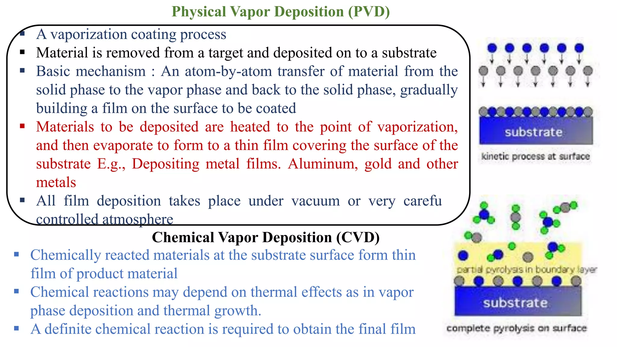
▪ A vaporization coating process
▪ Material is removed from a target and deposited on to a substrate
▪ Basic mechanism : An atom-by-atom transfer of material from the
solid phase to the vapor phase and back to the solid phase, gradually
building a film on the surface to be coated
▪ Materials to be deposited are heated to the point of vaporization,
and then evaporate to form to a thin film covering the surface of the
substrate E.g., Depositing metal films. Aluminum, gold and other
metals
▪ All film deposition takes place under vacuum or very carefully
controlled atmosphere
Physical Vapor Deposition (PVD)
▪ Chemically reacted materials at the substrate surface form thin
film of product material
▪ Chemical reactions may depend on thermal effects as in vapor
phase deposition and thermal growth.
▪ A definite chemical reaction is required to obtain the final film
Chemical Vapor Deposition (CVD)
Successive ionic layer adsorption and reaction (SILAR)
▪ Adsorptions of cations on surface of substrate
▪ Washing residue of electrolytes with the solvent
▪ Adsorptions pf anions on surface of substrate
▪ Washing residue of electrolytes with the solvent
▪ Among various chemical methods, the sequential
ionic layer adsorption reaction (SILAR) has been
shown to be one that most suitable for preparing
semiconductor materials
▪ A facile, low-cost growth method for the
fabrication semiconductors solar cells
o A binary semiconductor AB, where A - cation A+ and B -
anion, then ideally the lattice should have the atomic
arrangement of ABABAB·····.
o A SILAR process can produce such an arrangement by
sequential immersion of a substrate into a cationic solution
and an anionic solution
o Process can be repeated to increase the amount of deposited
material and the size of NCs
o In a real experiment, parameters such as solution
concentration, dipping time, temperature are crucial in
obtaining the desired semiconductor quality
Applications
▪ Semiconductors
▪ Oxide of metals
▪ nanocomposites
▪ polymer inorganic nanoparticles
composites
▪ porous materials & nanoparticles
Advantages
• Excellent material utilization efficiency
• Good control over the deposition
process along with the film thickness
• Cost effective and user friendly
• Large scale deposition capability on
virtually any type of substrate
• Easy control on film thickness by
adjusting number of deposition cycles is
the beauty of this method.
Precursors: Cadmium chloride CdCl2 solution
Sodium sulphide Na2S solution
Substrate: Precleaned Glass or FTO
Deposition parameters for getting adherent
thin films
▪ Concentration of the solution
▪ pH of the reacting baths,
▪ temperature of deposition
▪ Substrate treatment
▪ Deposition time
Under optimized deposition conditions
only, adherent thin films can be produced
Preparation of Cadmium sulphide CdS thin films
• A chemical dipping technique
• Involves successive dipping of a precleaned
substrate in separately placed cationic and
anionic precursor
• Between every immersion it is rinsed in ion
exchanged water
Na2S
solution
CdCl2
⋅2H2O]
solution
Adsorption of
cationic metal ions
Washing
Adsorption of
anionic ions
Reaction on the substrate
lead to the formation of
metal sulphide ion
Washing
Cadmium sulphide -optoelectronic applications
▪ solar cells
▪ photodiodes
▪ light emitting diodes
▪ nonlinear optics
▪ heterogeneous photocatalysis
▪ high-density magnetic information storage
Precursors: Cadmium acetate Cd(CH3COO)2 ⋅2H2O] solution
Ammonium sulphide [(NH4)2S] solution (OR)
Sodium sulphide Na2S solution
Substrate: Precleaned Glass or FTO
[(NH4)2S]
solution
Cd(CH3CO
O)2 ⋅2H2O]
solution
Adsorption of
cationic metal ions
Washing
Adsorption
of
anionic ions
CdS formation on the
substrate
Preparation of Cadmium sulphide CdS thin films
Cd(NO2)2 Cationic solution
Sodium sulphide Na2S solution
Washing
▪ The characteristics of thin films are very much
dependent on their thickness as the thickness of the
film resolves the performance of prepared thin films
▪ Thin films surface roughness, contact angle, adhesion
and intrinsic stress are the factors which decide the
efficiency of the operation of any device.
Significance of film thickness
1. Rosileschristopher, Andrea Cerdan-pasaran, Siraj Sidhik, Tzarara lopez luke , Improved performance of CdS quantum
dot sensitized solar cell by solvent modified SILAR approach (2018), Solar Energy 174:240-247,
DOI:10.1016/j.solener.2018.08.081
2. Partha Protim Chandra,Ayan Mukherjee, and P.Mitra, “Synthesis of Nanocrystalline CdS by SILAR and Their
Characterization”, Hindawi Publishing Corporation Journal of Materials Volume 2014
3. K. Veerathangam, Muthu Senthil Pandian, P. Ramasamy, “Influence of SILAR deposition cycles in CdS quantum dot-
sensitized solar cells” Journal of Materials Science: Materials in Electronics 29(9), DOI:10.1007/s10854-018-8721-0
4. B.R. Sankapal, R.S. Mane, C.D. Lokhande*, Deposition of CdS thin films by the successive ionic layer
5. adsorption and reaction (SILAR) method, Materials Research Bulletin 35 (2000) 177–184
6. B. Guzeldira, M. Saglama and A. Atesb, Deposition and Characterization of CdS, CuS and ZnS
7. Thin Films Deposited by SILAR Method, Vol. 121 (2012) ACTA PHYSICA POLONICA A No Proceedings of the
International Congress on Advances in Applied Physics and Materials Science, Antalya 2011
8. Jadhav U.M.1, Patel S.N.2 and Patil R.S.1*, Room Temperature Deposition of Nanocrystalline CdS Thin Film by
Successive Ionic Layer Adsorption and Reaction (SILAR) Method, Research Journal of Material Sciences
Vol. 1(1), 21-25, February (2013)
References
Thank you
Like!! Share!!

Preparation of thin films

  • 1.
    Preparation of thinfilms By SILAR method Washing R.Gandhimathi
  • 2.
    Thin - lessthan about one micron Film - layer of material on surface ▪ Thin films are ( low dimensional materials) thin material layers ranging from fractions of a nm to several m in thickness ▪ Created by condensing, species of matter (either by one by one atomic/molecular/ionic deposition ) ▪ Thin films, both crystalline and amorphous ▪ Thin film deposition is performed at very low pressures high vacuum Introduction to thin films • Solar cells • Light-emitting diodes • Photoconductors • Light crystal displays • Magneto-optic memories • Electro-optic coatings • Multilayer capacitors • Flat-panel displays • Smart windows • Computer chips • Magneto-optic discs • Lithography • Microelectromechanical systems (MEMS) • Multifunctional emerging coatings Applications of thin film technology
  • 3.
    ▪ Electronic semiconductordevices and optical coatings are the main applications benefiting from thin film construction ▪ Properties of material significantly differ when analyzed in the form of thin films ▪ Allows easy integration into various types of devices ▪ Key elements in the fields of optoelectronic, photonic, and magnetic devices Why thin films?
  • 4.
    Thin film depositionis the process of creating and depositing thin film coatings onto a substrate material To obtain thin films with good quality, there are different deposition techniques Thin film deposition techniques Thin film deposition • Movement of vaporized target atoms or molecules to the substrate • Formation of layers by atoms or molecule • Growth of the layered atoms or molecule Layer Island Layer + Island (Frank vander) (Merwe Volmer-Weber) (Stranski-Krastanov) Thin film Growth modes Atoms strongly bound to substrate Atoms strongly bound to each other Mixture of 1 & 2 Lattice mismatch induces Island formation
  • 5.
    Adatom: An atomintended to be adsorbed and incorporated on the surface Physisorption: Adsorption of the arriving atoms on the deposition surface through weak vander waals forces Surface diffusion: Diffusion of the physisorbed species on the surface before they get incorporated into the film Chemisorption: Reaction of the physisorbed species with each other and the deposition surface to form the bonds of the film material When island clusters coalesce/ combine, eventually form a continuous film Nucleation and growth
  • 6.
    ▪ A vaporizationcoating process ▪ Material is removed from a target and deposited on to a substrate ▪ Basic mechanism : An atom-by-atom transfer of material from the solid phase to the vapor phase and back to the solid phase, gradually building a film on the surface to be coated ▪ Materials to be deposited are heated to the point of vaporization, and then evaporate to form to a thin film covering the surface of the substrate E.g., Depositing metal films. Aluminum, gold and other metals ▪ All film deposition takes place under vacuum or very carefully controlled atmosphere Physical Vapor Deposition (PVD) ▪ Chemically reacted materials at the substrate surface form thin film of product material ▪ Chemical reactions may depend on thermal effects as in vapor phase deposition and thermal growth. ▪ A definite chemical reaction is required to obtain the final film Chemical Vapor Deposition (CVD)
  • 7.
    Successive ionic layeradsorption and reaction (SILAR) ▪ Adsorptions of cations on surface of substrate ▪ Washing residue of electrolytes with the solvent ▪ Adsorptions pf anions on surface of substrate ▪ Washing residue of electrolytes with the solvent ▪ Among various chemical methods, the sequential ionic layer adsorption reaction (SILAR) has been shown to be one that most suitable for preparing semiconductor materials ▪ A facile, low-cost growth method for the fabrication semiconductors solar cells o A binary semiconductor AB, where A - cation A+ and B - anion, then ideally the lattice should have the atomic arrangement of ABABAB·····. o A SILAR process can produce such an arrangement by sequential immersion of a substrate into a cationic solution and an anionic solution o Process can be repeated to increase the amount of deposited material and the size of NCs o In a real experiment, parameters such as solution concentration, dipping time, temperature are crucial in obtaining the desired semiconductor quality
  • 8.
    Applications ▪ Semiconductors ▪ Oxideof metals ▪ nanocomposites ▪ polymer inorganic nanoparticles composites ▪ porous materials & nanoparticles Advantages • Excellent material utilization efficiency • Good control over the deposition process along with the film thickness • Cost effective and user friendly • Large scale deposition capability on virtually any type of substrate • Easy control on film thickness by adjusting number of deposition cycles is the beauty of this method.
  • 9.
    Precursors: Cadmium chlorideCdCl2 solution Sodium sulphide Na2S solution Substrate: Precleaned Glass or FTO Deposition parameters for getting adherent thin films ▪ Concentration of the solution ▪ pH of the reacting baths, ▪ temperature of deposition ▪ Substrate treatment ▪ Deposition time Under optimized deposition conditions only, adherent thin films can be produced Preparation of Cadmium sulphide CdS thin films • A chemical dipping technique • Involves successive dipping of a precleaned substrate in separately placed cationic and anionic precursor • Between every immersion it is rinsed in ion exchanged water Na2S solution CdCl2 ⋅2H2O] solution Adsorption of cationic metal ions Washing Adsorption of anionic ions Reaction on the substrate lead to the formation of metal sulphide ion Washing
  • 10.
    Cadmium sulphide -optoelectronicapplications ▪ solar cells ▪ photodiodes ▪ light emitting diodes ▪ nonlinear optics ▪ heterogeneous photocatalysis ▪ high-density magnetic information storage Precursors: Cadmium acetate Cd(CH3COO)2 ⋅2H2O] solution Ammonium sulphide [(NH4)2S] solution (OR) Sodium sulphide Na2S solution Substrate: Precleaned Glass or FTO [(NH4)2S] solution Cd(CH3CO O)2 ⋅2H2O] solution Adsorption of cationic metal ions Washing Adsorption of anionic ions CdS formation on the substrate Preparation of Cadmium sulphide CdS thin films Cd(NO2)2 Cationic solution Sodium sulphide Na2S solution Washing ▪ The characteristics of thin films are very much dependent on their thickness as the thickness of the film resolves the performance of prepared thin films ▪ Thin films surface roughness, contact angle, adhesion and intrinsic stress are the factors which decide the efficiency of the operation of any device. Significance of film thickness
  • 11.
    1. Rosileschristopher, AndreaCerdan-pasaran, Siraj Sidhik, Tzarara lopez luke , Improved performance of CdS quantum dot sensitized solar cell by solvent modified SILAR approach (2018), Solar Energy 174:240-247, DOI:10.1016/j.solener.2018.08.081 2. Partha Protim Chandra,Ayan Mukherjee, and P.Mitra, “Synthesis of Nanocrystalline CdS by SILAR and Their Characterization”, Hindawi Publishing Corporation Journal of Materials Volume 2014 3. K. Veerathangam, Muthu Senthil Pandian, P. Ramasamy, “Influence of SILAR deposition cycles in CdS quantum dot- sensitized solar cells” Journal of Materials Science: Materials in Electronics 29(9), DOI:10.1007/s10854-018-8721-0 4. B.R. Sankapal, R.S. Mane, C.D. Lokhande*, Deposition of CdS thin films by the successive ionic layer 5. adsorption and reaction (SILAR) method, Materials Research Bulletin 35 (2000) 177–184 6. B. Guzeldira, M. Saglama and A. Atesb, Deposition and Characterization of CdS, CuS and ZnS 7. Thin Films Deposited by SILAR Method, Vol. 121 (2012) ACTA PHYSICA POLONICA A No Proceedings of the International Congress on Advances in Applied Physics and Materials Science, Antalya 2011 8. Jadhav U.M.1, Patel S.N.2 and Patil R.S.1*, Room Temperature Deposition of Nanocrystalline CdS Thin Film by Successive Ionic Layer Adsorption and Reaction (SILAR) Method, Research Journal of Material Sciences Vol. 1(1), 21-25, February (2013) References
  • 12.