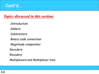
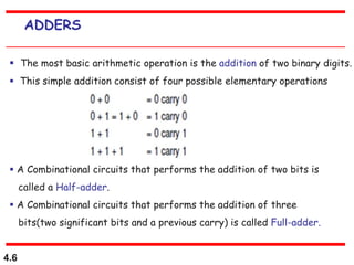
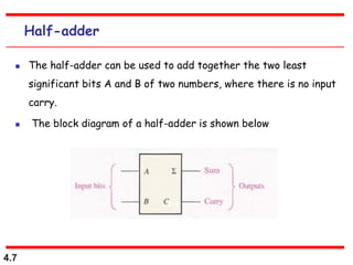
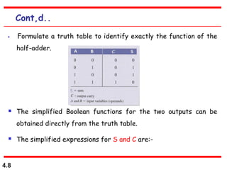
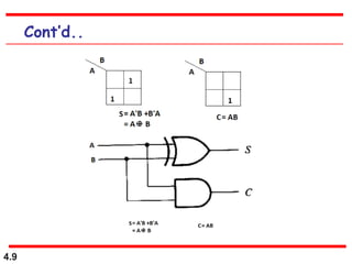
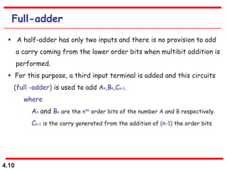
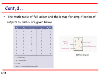
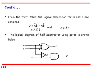
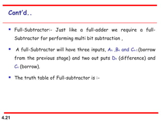
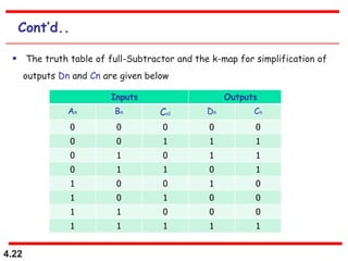
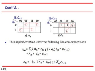
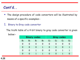
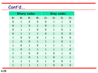
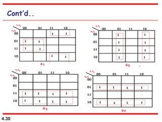
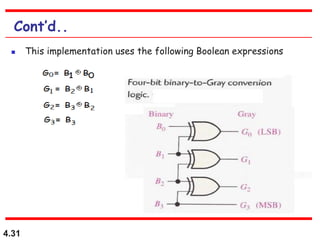
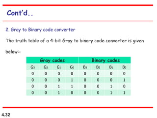
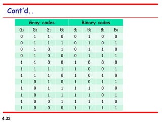
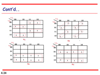
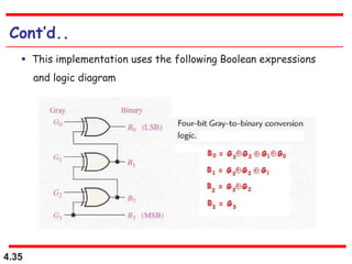
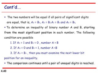
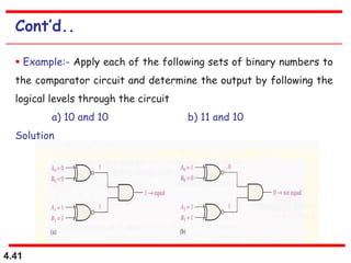
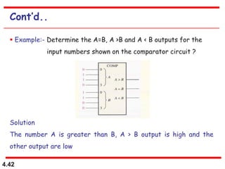
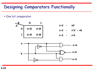
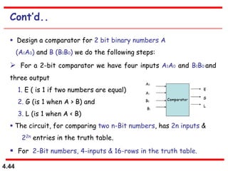
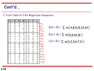
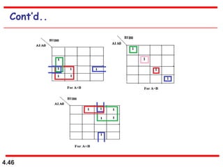
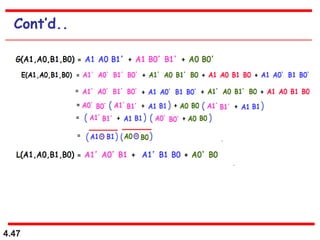
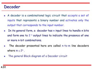
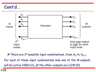
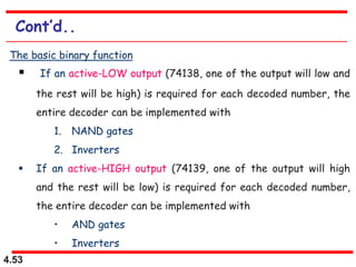
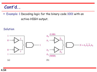
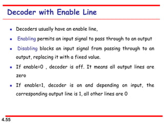
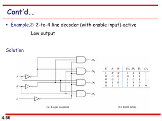
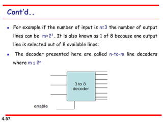
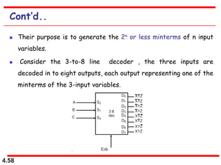
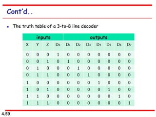
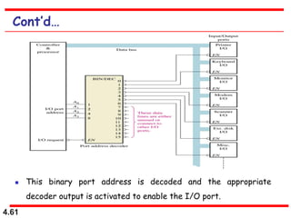
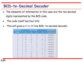
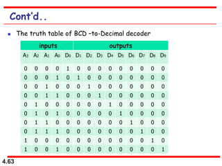
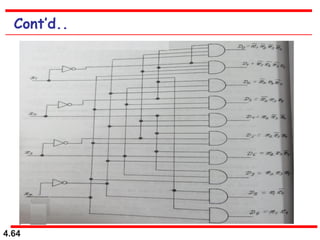
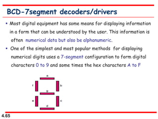
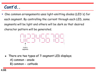
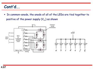
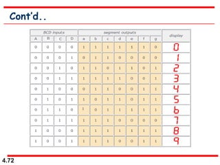
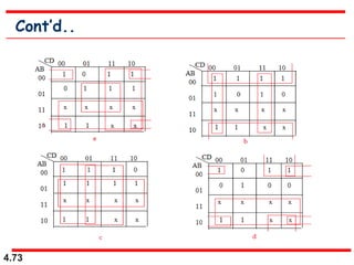
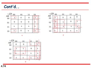
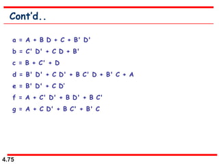
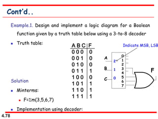
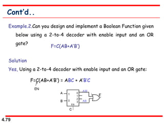
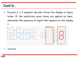
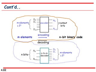
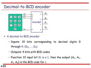
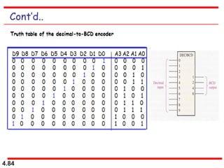
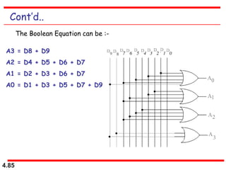
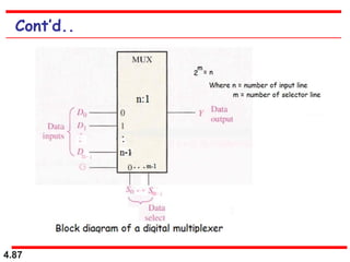
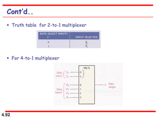
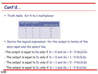
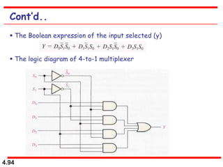
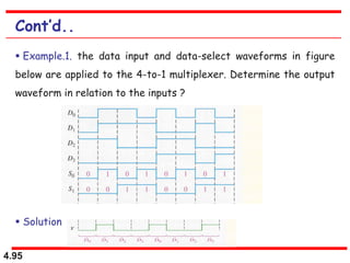
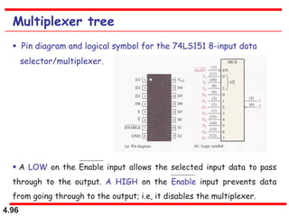
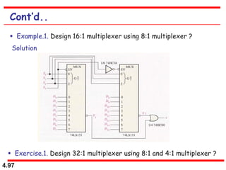
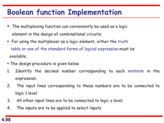
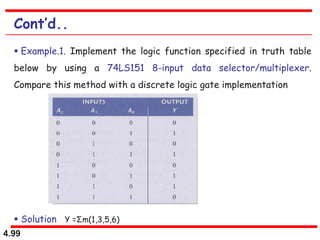
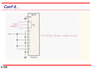
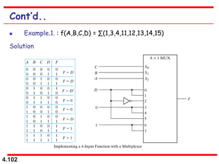
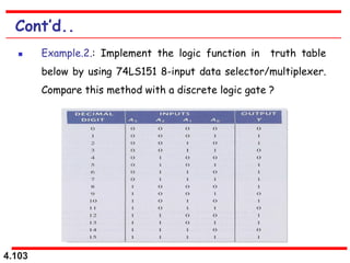
4.1
Under graduate (2016)
Girma Adam (M.Tech)
Chapter Four
Combinational
logic circuits
4.2
Topics discussed in this section:
Cont’d..
Introduction
Adders
Subtractors
Binary code conversion
Magnitude comparator
Decoders
Encoders
Multiplexers and Multiplexer tree
4.3
Introduction
 Basically the digital Circuits are divided in to two broad
categories
 Combinational Circuits
 Sequential Circuits
 A Combinational circuits consists of logical gates whose output
at any time are depending on the present combination of inputs.
 A block diagram of a combinational circuit is as shown below
4.4
Cont’d..
 The design of combinational circuits starts from the outline of
the problem and ends in a logical circuit diagram, or set Boolean
functions from which the logic diagram can be obtained.
 The procedure involves the following steps:-
 The problem is stated
 The number of both input and output variables required are
determined
 Both input and output variables are assigned letter symbols
 Te truth table that defines the required relationships
between input and outputs are derived.
4.5
Cont’d..
 The simplified Boolean function for each output is obtained.
 The logic diagram is drawn.
 A practical design method have to consider the following
requirements:-
1. Minimum number of gates
2. Minimum number of inputs to the gates
3. Minimum propagation delay
4. Minimum number of interconnection
5. High Speed of processing
6. Less Complexity
4.6
ADDERS
 The most basic arithmetic operation is the addition of two binary digits.
 This simple addition consist of four possible elementary operations
 A Combinational circuits that performs the addition of two bits is
called a Half-adder.
 A Combinational circuits that performs the addition of three
bits(two significant bits and a previous carry) is called Full-adder.
4.7
Half-adder
 The half-adder can be used to add together the two least
significant bits A and B of two numbers, where there is no input
carry.
 The block diagram of a half-adder is shown below
4.8
Cont,d..
 Formulate a truth table to identify exactly the function of the
half-adder.
 The simplified Boolean functions for the two outputs can be
obtained directly from the truth table.
 The simplified expressions for S and C are:-
4.9
Cont’d..
4.10
Full-adder
 A half-adder has only two inputs and there is no provision to add
a carry coming from the lower order bits when multibit addition is
performed.
 For this purpose, a third input terminal is added and this circuits
(full -adder) is used to add An,Bn,Cn-1.
where
An and Bn are the nth order bits of the number A and B respectively.
Cn-1 is the carry generated from the addition of (n-1) the order bits
4.11
Cont,d..
 The truth table of full-adder and the k-map for simplification of
outputs Sn and Cn are given below
4.12
Cont’d..
 This implementation uses the following Boolean expressions
4.13
Cont’d...
 The Sn output from the second half-adder is the exclusive-OR
of Cn-1 and the output of the first half-adder, giving
 Carry
4.14
Cont’d...
4.15
Full-adder from half-adders
4.16
Parallel adder
 Two or more full-adders are connected to form parallel binary
adders.
 The carry output signal from one stage propagates to the carry
input of the next stage
4.17
Cont,d..
 Example.1:- Determine the sum generated by the 3-bit parallel
adder and show the intermediate carriers when the binary
number 101 and 011 are being added ?
Solution
4.18
A 4-bit parallel binary adder
 Exercise 1:- Show how adders can be connected to form an 8-
bit parallel adder, and show the output bits for the following
input binary numbers ? 10111001 and 10011110
4.19
Subtractors
 Half-Subtractor:- a logical circuit for the subtraction of B
from A, where A and B are 1-bit numbers is referred to as a
half-Subtractor.
 The truth table of half-Subtractor is :-
 Here A and B are two inputs and D (difference) and C(borrow)
are the two outputs
4.20
Cont’d...
 From the truth table, the logical expression for D and C are
obtained
 The logical diagram of half-Subtractor using gates is shown
below
4.21
Cont’d..
 Full-Subtractor:- Just like a full-adder we require a full-
Subtractor for performing multi bit subtraction ,
 A full-Subtractor will have three inputs, An ,Bn and Cn-1 (borrow
from the previous stage) and two out puts Dn (difference) and
Cn (borrow).
 The truth table of Full-subtractor is :-
4.22
Cont’d..
Inputs Outputs
An Bn Cn1 Dn Cn
0 0 0 0 0
0 0 1 1 1
0 1 0 1 1
0 1 1 0 1
1 0 0 1 0
1 0 1 0 0
1 1 0 0 0
1 1 1 1 1
 The truth table of full-Subtractor and the k-map for simplification of
outputs Dn and Cn are given below
4.23
Cont’d..
 This implementation uses the following Boolean expressions
4.24
Cont’d..
 The full – Subtractor logic Circuit diagram
4.25
Binary Subtractor using 2’s complement
 The Subtrcation A – B can be done by taking the 2’s
complement of B and adding it to A because A- B = A + (-B) =
A+2’sB.
 It means if we use the inverters to make 1’s complement of B
(connecting each Bi to an inverter) and then add 1 to the
least significant bit (by setting carry C0 to 1) of binary
adder, then we can make a binary subtractor.
4.26
4 bit 2’s complement Subtractor
4.27
Binary Conversion
 The availability of a large variety of codes for the same
discrete elements of information results in the use of different
codes by different digital systems.
 It is sometimes necessary to use the output of one system as
input to another , at this condition a conversion circuit is
inserted between the two systems, if each uses different codes
for the same information.
 Thus a code converter is a circuit that makes the two systems
compatible even though each system uses a different binary
code.
4.28
Cont’d..
 The design procedure of code converters will be illustrated by
means of a specific examples:-
1. Binary to Gray code converter
The truth table of a 4-bit binary to gray code converter is given
below:-
Binary codes Gray codes
B3 B2 B1 B0 G3 G2 G1 G0
0 0 0 0 0 0 0 0
0 0 0 1 0 0 0 1
0 0 1 0 0 0 1 1
0 0 1 1 0 0 1 0
4.29
Cont’d..
Binary codes Gray codes
B3 B2 B1 B0 G3 G2 G1 G0
0 1 0 0 0 1 1 0
0 1 0 1 0 1 1 1
0 1 1 0 0 1 0 1
0 1 1 1 0 1 0 0
1 0 0 0 1 1 0 0
1 0 0 1 1 1 0 1
1 0 1 0 1 1 1 1
1 0 1 1 1 1 1 0
1 1 0 0 1 0 1 0
1 1 0 1 1 0 1 1
1 1 1 0 1 0 0 1
1 1 1 1 1 0 0 0
4.30
Cont’d..
4.31
Cont’d..
 This implementation uses the following Boolean expressions
4.32
Cont’d..
2. Gray to Binary code converter
The truth table of a 4-bit Gray to binary code converter is given
below:-
Gray codes Binary codes
G3 G2 G1 G0 B3 B2 B1 B0
0 0 0 0 0 0 0 0
0 0 0 1 0 0 0 1
0 0 1 1 0 0 1 0
0 0 1 0 0 0 1 1
4.33
Cont’d..
Gray codes Binary codes
G3 G2 G1 G0 B3 B2 B1 B0
0 1 1 0 0 1 0 0
0 1 1 1 0 1 0 1
0 1 0 1 0 1 1 0
0 1 0 0 0 1 1 1
1 1 0 0 1 0 0 0
1 1 1 1 1 0 0 1
1 1 1 0 1 0 1 0
1 0 1 0 1 0 1 1
1 0 1 1 1 1 0 0
1 0 1 1 1 1 0 1
1 0 0 1 1 1 1 0
1 0 0 0 1 1 1 1
4.34
Cont’d..
4.35
Cont’d..
 This implementation uses the following Boolean expressions
and logic diagram
4.36
Cont’d..
 Exercise
1. Convert the binary number 0101 to Gray code with
exclusive –OR gates
2. Convert the Gray code 1011 to binary with
exclusive –OR gates
Solution
4.37
Magnitude comparator
 A magnitude comparator is a combinational circuit that compares
two numbers A and B, and determines their relative magnitudes.
 The outcome of the comparison is specified by three binary
variables that indicate whether A> B, A=B or A<B.
 Exclusive-OR gate can be used as a basic comparator
1. Equality
Exclusive-OR gate as 1-bit comparator
4.38
Cont’d..
 Exclusive-OR gate as 2-bit comparator
 The output is 1 when Ao=Bo and A1=B1,
4.39
Cont’d..
 Exclusive-OR gate as 4-bit comparator
 Detects one of three conditions
 Only one output will be High at any one time
- A greater than B (A > B)
- A equal to B (A = B)
- A less than B (A < B)
4.40
Cont’d..
 The two numbers will be equal if all pairs of significant digits
are equal, that is, A3 = B3, A2 = B2,A1 = B1 and A0 = B0.
 To determine an inequality of binary number A and B, starting
from the most significant position in each number. The following
condition are possible
1. If A3 = 1 and B3 = 0 , number A > B
2. If A3 = 0 and B3 = 1, number A <B
3. If A3 = B3 , then you must examine the next lower bit
position for an inequality.
 The comparison continues until a pair of unequal digits is reached.
4.41
Cont’d..
 Example:- Apply each of the following sets of binary numbers to
the comparator circuit and determine the output by following the
logical levels through the circuit
a) 10 and 10 b) 11 and 10
Solution
4.42
Cont’d..
 Example:- Determine the A=B, A >B and A < B outputs for the
input numbers shown on the comparator circuit ?
Solution
The number A is greater than B, A > B output is high and the
other output are low
4.43
Designing Comparators Functionally
 One bit comparator
4.44
Cont’d..
 Design a comparator for 2 bit binary numbers A
(A1A0) and B (B1B0) we do the following steps:
 For a 2-bit comparator we have four inputs A1A0 and B1B0 and
three output
1. E ( is 1 if two numbers are equal)
2. G (is 1 when A > B) and
3. L (is 1 when A < B)
 The circuit, for comparing two n-Bit numbers, has 2n inputs &
22n entries in the truth table.
 For 2-Bit numbers, 4-inputs & 16-rows in the truth table.
4.45
Cont’d..
 Truth Table of 2-Bit Magnitude Comparator
4.46
Cont’d..
4.47
Cont’d..
4.48
Cont’d..
4.49
Cont’d..
4.50
Combined
4.51
Decoder
 A decoder is a combinational logic circuit that accepts a set of
inputs that represents a binary number and activates only the
output that corresponds to the input number.
 In its general form, a decoder has n input lines to handle n bits
and form one to 2 n output lines to indicate the presence of one
or more n-bit combinations.
 The decoder presented here are called n-to-m line decoders
where m ≤ 2n .
 The general Block diagram of a Decoder circuit
4.52
Cont’d..
# There are 2N possible input combinations, from A0 to AN1.
For each of these input combinations only one of the M outputs
will be active HIGH (1), all the other outputs are LOW (0).
4.53
Cont’d..
The basic binary function
 If an active-LOW output (74138, one of the output will low and
the rest will be high) is required for each decoded number, the
entire decoder can be implemented with
1. NAND gates
2. Inverters
 If an active-HIGH output (74139, one of the output will high
and the rest will be low) is required for each decoded number,
the entire decoder can be implemented with
• AND gates
• Inverters
4.54
Cont’d..
 Example: 1 Decoding logic for the binary code 1001 with an
active-HIGH output.
Solution
4.55
Decoder with Enable Line
 Decoders usually have an enable line,
 Enabling permits an input signal to pass through to an output
 Disabling blocks an input signal from passing through to an
output, replacing it with a fixed value.
 If enable=0 , decoder is off. It means all output lines are
zero
 If enable=1, decoder is on and depending on input, the
corresponding output line is 1, all other lines are 0
4.56
Cont’d..
 Example.2: 2-to-4 line decoder (with enable input)-active
Low output
Solution
4.57
Cont’d..
 For example if the number of input is n=3 the number of output
lines can be m=23 . It is also known as 1 of 8 because one output
line is selected out of 8 available lines:
 The decoder presented here are called n-to-m line decoders
where m ≤ 2n
4.58
Cont’d..
 Their purpose is to generate the 2n or less minterms of n input
variables.
 Consider the 3-to-8 line decoder , the three inputs are
decoded in to eight outputs, each output representing one of the
minterms of the 3-input variables.
4.59
Cont’d..
 The truth table of a 3-to-8 line decoder
4.60
Cont’d..
4.61
Cont’d…
 This binary port address is decoded and the appropriate
decoder output is activated to enable the I/O port.
4.62
BCD-to-Decimal Decoder
 The elements of information in this case are the ten decimal
digits represented by the BCD code.
 The code itself has four bits
 This will gives a 4-to-10 line BCD –to-decimal decoder.
4.63
Cont’d..
 The truth table of BCD –to-Decimal decoder
inputs outputs
A3 A2 A1 A0 D0 D1 D2 D3 D4 D5 D6 D7 D8 D9
0 0 0 0 1 0 0 0 0 0 0 0 0 0
0 0 0 1 0 1 0 0 0 0 0 0 0 0
0 0 1 0 0 0 1 0 0 0 0 0 0 0
0 0 1 1 0 0 0 1 0 0 0 0 0 0
0 1 0 0 0 0 0 0 1 0 0 0 0 0
0 1 0 1 0 0 0 0 0 1 0 0 0 0
0 1 1 0 0 0 0 0 0 0 1 0 0 0
0 1 1 1 0 0 0 0 0 0 0 1 0 0
1 0 0 0 0 0 0 0 0 0 0 0 1 0
1 0 0 1 0 0 0 0 0 0 0 0 0 1
4.64
Cont’d..
4.65
BCD-7segment decoders/drivers
 Most digital equipment has some means for displaying information
in a form that can be understood by the user. This information is
often numerical data but also be alphanumeric.
 One of the simplest and most popular methods for displaying
numerical digits uses a 7-segment configuration to form digital
characters 0 to 9 and some times the hex characters A to F
4.66
Cont’d..
 One common arrangements uses light-emitting diodes (LED's) for
each segment. By controlling the current through each LED, some
segments will be light and others will be dark so that desired
character pattern will be generated.
 There are two types of 7segment LED displays;
A) common - anode
B) common  cathode
4.67
Cont’d..
 In commonanode, the anode of all of the LEDs are tied together to
positive of the power supply (Vcc) as shown
4.68
Cont’d..
4.69
Cont’d..
 Example: 1
4.70
Cont’d..
4.71
Cont’d..
 In common cathode, the cathode of all of the LEDs are tied together
to positive of the power supply (Vcc) as shown
4.72
Cont’d..
4.73
Cont’d..
4.74
Cont’d..
4.75
Cont’d..
a = A + B D + C + B' D'
b = C' D' + C D + B'
c = B + C' + D
d = B' D' + C D' + B C' D + B' C + A
e = B' D' + C D’
f = A + C' D' + B D' + B C'
g = A + C D' + B C' + B' C
4.76
Cont’d..
4.77
Cont’d..
4.78
Cont’d..
Example.1. Design and implement a logic diagram for a Boolean
function given by a truth table below using a 3-to-8 decoder
 Truth table:
Solution
 Minterms:
 F=m(3,5,6,7)
 Implementation using decoder:
A B C F
0 0 0 0
0 0 1 0
0 1 0 0
0 1 1 1
1 0 0 0
1 0 1 1
1 1 0 1
1 1 1 1
0
1
2
3
4
5
6
7
A
B
C
2
1
0
F
Indicate MSB, LSB
4.79
Cont’d..
Example.2.Can you design and implement a Boolean Function given
below using a 2-to-4 decoder with enable input and an OR
gate?
Solution
Yes, Using a 2-to-4 decoder with enable input and an OR gate:
F=C(AB+A’B’)
F=C(AB+A’B’) = ABC + A’B’C
EN
4.80
Cont’d..
 Example.3. a 7-segment decoder drives the display in figure
below. If the waveforms given below are applied as input,
determine the sequence of digits that appears on the display
?
 Solution
4.81
Encoder
 An encoder is a combinational logic circuit that essentially
performs a ‘’ reverse’’ process of decoder function.
 Encoders can encode various symbols and alphabetic
characters.
 The process of converting from familiar symbols or number
to a coded format is called encoding.
 An encoder accepts an active level on one of its inputs
representing a digit, such as a decimal or octal and converts
it to a coded output, such as BCD or Binary
4.82
Cont’d..
4.83
Decimal-to-BCD encoder
 A decimal-to-BCD encoder
• Inputs: 10 bits corresponding to decimal digits 0
through 9, (D0, …, D9)
• Outputs: 4 bits with BCD codes
• Function: If input bit Di is a 1, then the output (A3, A2,
A1, A0) is the BCD code for i,
4.84
Cont’d..
4.85
Cont’d..
A3 = D8 + D9
A2 = D4 + D5 + D6 + D7
A1 = D2 + D3 + D6 + D7
A0 = D1 + D3 + D5 + D7 + D9
The Boolean Equation can be :-
4.86
Multiplexer & Multiplexer tree
 It is a combinational circuit that selects binary information
from one of the input lines and directs it to a single output line
 Usually there are 2n input lines and n selection lines whose bit
combinations determine which input line is selected
 Depending upon the digital code applied at the selector inputs
one out of n data source is selected and transmitted to a single
output channel.
4.87
Cont’d..
4.88
Cont’d..
 MUX Types
 2-to-1 (1 select line)
 4-to-1 (2 select lines)
 8-to-1 (3 select lines)
 16-to-1 (4 select lines)
4.89
Typical Application of a MUX
4.90
Cont’d..
4.91
Cont’d..
 For example for 2-to-1 multiplexer
1. if selection S is zero then I0 has the path to output and
2. if S is one I1 has the path to output
4.92
Cont’d..
 Truth table for 2-to-1 multiplexer
 For 4-to-1 multiplexer
4.93
Cont’d..
 Truth table for 4-to-1 multiplexer
 Derive the logical expression for the output in terms of the
data input and the select line
-The output is equal to Do only if S1 = 0 and So = 0 : Y=DoS1So
- The output is equal to D1 only if S1 = 0 and So = 1 : Y=D1S1So
- The output is equal to D2 only if S1 = 1 and So = 0 : Y=D2S1So
- The output is equal to D3 only if S1 = 1 and So = 1 : Y=D3S1So
4.94
Cont’d..
 The Boolean expression of the input selected (y)
 The logic diagram of 4-to-1 multiplexer
4.95
Cont’d..
 Example.1. the data input and data-select waveforms in figure
below are applied to the 4-to-1 multiplexer. Determine the output
waveform in relation to the inputs ?
 Solution
4.96
Multiplexer tree
 Pin diagram and logical symbol for the 74LS151 8-input data
selector/multiplexer.
 A LOW on the Enable input allows the selected input data to pass
through to the output. A HIGH on the Enable input prevents data
from going through to the output; i.e, it disables the multiplexer.
4.97
Cont’d..
 Example.1. Design 16:1 multiplexer using 8:1 multiplexer ?
Solution
 Exercise.1. Design 32:1 multiplexer using 8:1 and 4:1 multiplexer ?
4.98
Boolean function Implementation
 The multiplexing function can conveniently be used as a logic
element in the design of combinational circuits.
 For using the multiplexer as a logic element, either the truth
table or one of the standard forms of logical expression must be
available.
 The design procedure is given below
1. Identify the decimal number corresponding to each minterm in the
expression.
2. The input lines corresponding to these numbers are to be connected to
logic 1 level.
3. All other input lines are to be connected to logic o level.
4. The inputs are to be applied to select inputs
4.99
Cont’d..
 Example.1. Implement the logic function specified in truth table
below by using a 74LS151 8-input data selector/multiplexer.
Compare this method with a discrete logic gate implementation
 Solution Y =Σm(1,3,5,6)
4.100
Cont’d..
4.101
Cont’d..
 Another method for implementing Boolean function is using
multiplexer
 For doing that assume Boolean function has n variables. We
have to use multiplexer with n-1 selection lines and
 1- first n-1 variables of function is used for data input
 2- the remaining single variable ( named z )is used for data
input.
 Each data input can be z, z’, 1 or 0. From truth table we
have to find the relation of F and z to be able to design
input lines.
4.102
Cont’d..
 Example.1. : f(A,B,C,D) = ∑(1,3,4,11,12,13,14,15)
Solution
4.103
Cont’d..
 Example.2.: Implement the logic function in truth table
below by using 74LS151 8-input data selector/multiplexer.
Compare this method with a discrete logic gate ?
4.104
Cont’d..
 Solution
4.105
Demultiplexer
 A demultiplexer basically reverse the multiplexing function. It
takes digital information from one line and distributes it to a given
number of outputs. For this reason the demultiplexer is also know
as data distributor.
4.106
Cont’d..
 DEMUX Types
 1-to-2 (1 select line)
 1-to-4 (2 select lines)
 1-to-8 (3 select lines)
 1-to-16 (4 select lines)
4.107
Typical Application of a DEMUX
4.108
Cont’d..
 For example for 1-to-4 De-Multiplexer (DEMUX)
4.109
Cont’d..
 Example.1. The serial data-input wave form(data in) and data-
select inputs (So and S1) are as shown below. Determine the data-
output waveforms for the 1-to-4 demultiplexer ?
 Solution

DLD Chapter-4.pdf

  • 1.
    4.1 Under graduate (2016) GirmaAdam (M.Tech) Chapter Four Combinational logic circuits
  • 2.
    4.2 Topics discussed inthis section: Cont’d.. Introduction Adders Subtractors Binary code conversion Magnitude comparator Decoders Encoders Multiplexers and Multiplexer tree
  • 3.
    4.3 Introduction  Basically thedigital Circuits are divided in to two broad categories  Combinational Circuits  Sequential Circuits  A Combinational circuits consists of logical gates whose output at any time are depending on the present combination of inputs.  A block diagram of a combinational circuit is as shown below
  • 4.
    4.4 Cont’d..  The designof combinational circuits starts from the outline of the problem and ends in a logical circuit diagram, or set Boolean functions from which the logic diagram can be obtained.  The procedure involves the following steps:-  The problem is stated  The number of both input and output variables required are determined  Both input and output variables are assigned letter symbols  Te truth table that defines the required relationships between input and outputs are derived.
  • 5.
    4.5 Cont’d..  The simplifiedBoolean function for each output is obtained.  The logic diagram is drawn.  A practical design method have to consider the following requirements:- 1. Minimum number of gates 2. Minimum number of inputs to the gates 3. Minimum propagation delay 4. Minimum number of interconnection 5. High Speed of processing 6. Less Complexity
  • 6.
    4.6 ADDERS  The mostbasic arithmetic operation is the addition of two binary digits.  This simple addition consist of four possible elementary operations  A Combinational circuits that performs the addition of two bits is called a Half-adder.  A Combinational circuits that performs the addition of three bits(two significant bits and a previous carry) is called Full-adder.
  • 7.
    4.7 Half-adder  The half-addercan be used to add together the two least significant bits A and B of two numbers, where there is no input carry.  The block diagram of a half-adder is shown below
  • 8.
    4.8 Cont,d..  Formulate atruth table to identify exactly the function of the half-adder.  The simplified Boolean functions for the two outputs can be obtained directly from the truth table.  The simplified expressions for S and C are:-
  • 9.
  • 10.
    4.10 Full-adder  A half-adderhas only two inputs and there is no provision to add a carry coming from the lower order bits when multibit addition is performed.  For this purpose, a third input terminal is added and this circuits (full -adder) is used to add An,Bn,Cn-1. where An and Bn are the nth order bits of the number A and B respectively. Cn-1 is the carry generated from the addition of (n-1) the order bits
  • 11.
    4.11 Cont,d..  The truthtable of full-adder and the k-map for simplification of outputs Sn and Cn are given below
  • 12.
    4.12 Cont’d..  This implementationuses the following Boolean expressions
  • 13.
    4.13 Cont’d...  The Snoutput from the second half-adder is the exclusive-OR of Cn-1 and the output of the first half-adder, giving  Carry
  • 14.
  • 15.
  • 16.
    4.16 Parallel adder  Twoor more full-adders are connected to form parallel binary adders.  The carry output signal from one stage propagates to the carry input of the next stage
  • 17.
    4.17 Cont,d..  Example.1:- Determinethe sum generated by the 3-bit parallel adder and show the intermediate carriers when the binary number 101 and 011 are being added ? Solution
  • 18.
    4.18 A 4-bit parallelbinary adder  Exercise 1:- Show how adders can be connected to form an 8- bit parallel adder, and show the output bits for the following input binary numbers ? 10111001 and 10011110
  • 19.
    4.19 Subtractors  Half-Subtractor:- alogical circuit for the subtraction of B from A, where A and B are 1-bit numbers is referred to as a half-Subtractor.  The truth table of half-Subtractor is :-  Here A and B are two inputs and D (difference) and C(borrow) are the two outputs
  • 20.
    4.20 Cont’d...  From thetruth table, the logical expression for D and C are obtained  The logical diagram of half-Subtractor using gates is shown below
  • 21.
    4.21 Cont’d..  Full-Subtractor:- Justlike a full-adder we require a full- Subtractor for performing multi bit subtraction ,  A full-Subtractor will have three inputs, An ,Bn and Cn-1 (borrow from the previous stage) and two out puts Dn (difference) and Cn (borrow).  The truth table of Full-subtractor is :-
  • 22.
    4.22 Cont’d.. Inputs Outputs An BnCn1 Dn Cn 0 0 0 0 0 0 0 1 1 1 0 1 0 1 1 0 1 1 0 1 1 0 0 1 0 1 0 1 0 0 1 1 0 0 0 1 1 1 1 1  The truth table of full-Subtractor and the k-map for simplification of outputs Dn and Cn are given below
  • 23.
    4.23 Cont’d..  This implementationuses the following Boolean expressions
  • 24.
    4.24 Cont’d..  The full– Subtractor logic Circuit diagram
  • 25.
    4.25 Binary Subtractor using2’s complement  The Subtrcation A – B can be done by taking the 2’s complement of B and adding it to A because A- B = A + (-B) = A+2’sB.  It means if we use the inverters to make 1’s complement of B (connecting each Bi to an inverter) and then add 1 to the least significant bit (by setting carry C0 to 1) of binary adder, then we can make a binary subtractor.
  • 26.
    4.26 4 bit 2’scomplement Subtractor
  • 27.
    4.27 Binary Conversion  Theavailability of a large variety of codes for the same discrete elements of information results in the use of different codes by different digital systems.  It is sometimes necessary to use the output of one system as input to another , at this condition a conversion circuit is inserted between the two systems, if each uses different codes for the same information.  Thus a code converter is a circuit that makes the two systems compatible even though each system uses a different binary code.
  • 28.
    4.28 Cont’d..  The designprocedure of code converters will be illustrated by means of a specific examples:- 1. Binary to Gray code converter The truth table of a 4-bit binary to gray code converter is given below:- Binary codes Gray codes B3 B2 B1 B0 G3 G2 G1 G0 0 0 0 0 0 0 0 0 0 0 0 1 0 0 0 1 0 0 1 0 0 0 1 1 0 0 1 1 0 0 1 0
  • 29.
    4.29 Cont’d.. Binary codes Graycodes B3 B2 B1 B0 G3 G2 G1 G0 0 1 0 0 0 1 1 0 0 1 0 1 0 1 1 1 0 1 1 0 0 1 0 1 0 1 1 1 0 1 0 0 1 0 0 0 1 1 0 0 1 0 0 1 1 1 0 1 1 0 1 0 1 1 1 1 1 0 1 1 1 1 1 0 1 1 0 0 1 0 1 0 1 1 0 1 1 0 1 1 1 1 1 0 1 0 0 1 1 1 1 1 1 0 0 0
  • 30.
  • 31.
    4.31 Cont’d..  This implementationuses the following Boolean expressions
  • 32.
    4.32 Cont’d.. 2. Gray toBinary code converter The truth table of a 4-bit Gray to binary code converter is given below:- Gray codes Binary codes G3 G2 G1 G0 B3 B2 B1 B0 0 0 0 0 0 0 0 0 0 0 0 1 0 0 0 1 0 0 1 1 0 0 1 0 0 0 1 0 0 0 1 1
  • 33.
    4.33 Cont’d.. Gray codes Binarycodes G3 G2 G1 G0 B3 B2 B1 B0 0 1 1 0 0 1 0 0 0 1 1 1 0 1 0 1 0 1 0 1 0 1 1 0 0 1 0 0 0 1 1 1 1 1 0 0 1 0 0 0 1 1 1 1 1 0 0 1 1 1 1 0 1 0 1 0 1 0 1 0 1 0 1 1 1 0 1 1 1 1 0 0 1 0 1 1 1 1 0 1 1 0 0 1 1 1 1 0 1 0 0 0 1 1 1 1
  • 34.
  • 35.
    4.35 Cont’d..  This implementationuses the following Boolean expressions and logic diagram
  • 36.
    4.36 Cont’d..  Exercise 1. Convertthe binary number 0101 to Gray code with exclusive –OR gates 2. Convert the Gray code 1011 to binary with exclusive –OR gates Solution
  • 37.
    4.37 Magnitude comparator  Amagnitude comparator is a combinational circuit that compares two numbers A and B, and determines their relative magnitudes.  The outcome of the comparison is specified by three binary variables that indicate whether A> B, A=B or A<B.  Exclusive-OR gate can be used as a basic comparator 1. Equality Exclusive-OR gate as 1-bit comparator
  • 38.
    4.38 Cont’d..  Exclusive-OR gateas 2-bit comparator  The output is 1 when Ao=Bo and A1=B1,
  • 39.
    4.39 Cont’d..  Exclusive-OR gateas 4-bit comparator  Detects one of three conditions  Only one output will be High at any one time - A greater than B (A > B) - A equal to B (A = B) - A less than B (A < B)
  • 40.
    4.40 Cont’d..  The twonumbers will be equal if all pairs of significant digits are equal, that is, A3 = B3, A2 = B2,A1 = B1 and A0 = B0.  To determine an inequality of binary number A and B, starting from the most significant position in each number. The following condition are possible 1. If A3 = 1 and B3 = 0 , number A > B 2. If A3 = 0 and B3 = 1, number A <B 3. If A3 = B3 , then you must examine the next lower bit position for an inequality.  The comparison continues until a pair of unequal digits is reached.
  • 41.
    4.41 Cont’d..  Example:- Applyeach of the following sets of binary numbers to the comparator circuit and determine the output by following the logical levels through the circuit a) 10 and 10 b) 11 and 10 Solution
  • 42.
    4.42 Cont’d..  Example:- Determinethe A=B, A >B and A < B outputs for the input numbers shown on the comparator circuit ? Solution The number A is greater than B, A > B output is high and the other output are low
  • 43.
  • 44.
    4.44 Cont’d..  Design acomparator for 2 bit binary numbers A (A1A0) and B (B1B0) we do the following steps:  For a 2-bit comparator we have four inputs A1A0 and B1B0 and three output 1. E ( is 1 if two numbers are equal) 2. G (is 1 when A > B) and 3. L (is 1 when A < B)  The circuit, for comparing two n-Bit numbers, has 2n inputs & 22n entries in the truth table.  For 2-Bit numbers, 4-inputs & 16-rows in the truth table.
  • 45.
    4.45 Cont’d..  Truth Tableof 2-Bit Magnitude Comparator
  • 46.
  • 47.
  • 48.
  • 49.
  • 50.
  • 51.
    4.51 Decoder  A decoderis a combinational logic circuit that accepts a set of inputs that represents a binary number and activates only the output that corresponds to the input number.  In its general form, a decoder has n input lines to handle n bits and form one to 2 n output lines to indicate the presence of one or more n-bit combinations.  The decoder presented here are called n-to-m line decoders where m ≤ 2n .  The general Block diagram of a Decoder circuit
  • 52.
    4.52 Cont’d.. # There are2N possible input combinations, from A0 to AN1. For each of these input combinations only one of the M outputs will be active HIGH (1), all the other outputs are LOW (0).
  • 53.
    4.53 Cont’d.. The basic binaryfunction  If an active-LOW output (74138, one of the output will low and the rest will be high) is required for each decoded number, the entire decoder can be implemented with 1. NAND gates 2. Inverters  If an active-HIGH output (74139, one of the output will high and the rest will be low) is required for each decoded number, the entire decoder can be implemented with • AND gates • Inverters
  • 54.
    4.54 Cont’d..  Example: 1Decoding logic for the binary code 1001 with an active-HIGH output. Solution
  • 55.
    4.55 Decoder with EnableLine  Decoders usually have an enable line,  Enabling permits an input signal to pass through to an output  Disabling blocks an input signal from passing through to an output, replacing it with a fixed value.  If enable=0 , decoder is off. It means all output lines are zero  If enable=1, decoder is on and depending on input, the corresponding output line is 1, all other lines are 0
  • 56.
    4.56 Cont’d..  Example.2: 2-to-4line decoder (with enable input)-active Low output Solution
  • 57.
    4.57 Cont’d..  For exampleif the number of input is n=3 the number of output lines can be m=23 . It is also known as 1 of 8 because one output line is selected out of 8 available lines:  The decoder presented here are called n-to-m line decoders where m ≤ 2n
  • 58.
    4.58 Cont’d..  Their purposeis to generate the 2n or less minterms of n input variables.  Consider the 3-to-8 line decoder , the three inputs are decoded in to eight outputs, each output representing one of the minterms of the 3-input variables.
  • 59.
    4.59 Cont’d..  The truthtable of a 3-to-8 line decoder
  • 60.
  • 61.
    4.61 Cont’d…  This binaryport address is decoded and the appropriate decoder output is activated to enable the I/O port.
  • 62.
    4.62 BCD-to-Decimal Decoder  Theelements of information in this case are the ten decimal digits represented by the BCD code.  The code itself has four bits  This will gives a 4-to-10 line BCD –to-decimal decoder.
  • 63.
    4.63 Cont’d..  The truthtable of BCD –to-Decimal decoder inputs outputs A3 A2 A1 A0 D0 D1 D2 D3 D4 D5 D6 D7 D8 D9 0 0 0 0 1 0 0 0 0 0 0 0 0 0 0 0 0 1 0 1 0 0 0 0 0 0 0 0 0 0 1 0 0 0 1 0 0 0 0 0 0 0 0 0 1 1 0 0 0 1 0 0 0 0 0 0 0 1 0 0 0 0 0 0 1 0 0 0 0 0 0 1 0 1 0 0 0 0 0 1 0 0 0 0 0 1 1 0 0 0 0 0 0 0 1 0 0 0 0 1 1 1 0 0 0 0 0 0 0 1 0 0 1 0 0 0 0 0 0 0 0 0 0 0 1 0 1 0 0 1 0 0 0 0 0 0 0 0 0 1
  • 64.
  • 65.
    4.65 BCD-7segment decoders/drivers  Mostdigital equipment has some means for displaying information in a form that can be understood by the user. This information is often numerical data but also be alphanumeric.  One of the simplest and most popular methods for displaying numerical digits uses a 7-segment configuration to form digital characters 0 to 9 and some times the hex characters A to F
  • 66.
    4.66 Cont’d..  One commonarrangements uses light-emitting diodes (LED's) for each segment. By controlling the current through each LED, some segments will be light and others will be dark so that desired character pattern will be generated.  There are two types of 7segment LED displays; A) common - anode B) common  cathode
  • 67.
    4.67 Cont’d..  In commonanode,the anode of all of the LEDs are tied together to positive of the power supply (Vcc) as shown
  • 68.
  • 69.
  • 70.
  • 71.
    4.71 Cont’d..  In commoncathode, the cathode of all of the LEDs are tied together to positive of the power supply (Vcc) as shown
  • 72.
  • 73.
  • 74.
  • 75.
    4.75 Cont’d.. a = A+ B D + C + B' D' b = C' D' + C D + B' c = B + C' + D d = B' D' + C D' + B C' D + B' C + A e = B' D' + C D’ f = A + C' D' + B D' + B C' g = A + C D' + B C' + B' C
  • 76.
  • 77.
  • 78.
    4.78 Cont’d.. Example.1. Design andimplement a logic diagram for a Boolean function given by a truth table below using a 3-to-8 decoder  Truth table: Solution  Minterms:  F=m(3,5,6,7)  Implementation using decoder: A B C F 0 0 0 0 0 0 1 0 0 1 0 0 0 1 1 1 1 0 0 0 1 0 1 1 1 1 0 1 1 1 1 1 0 1 2 3 4 5 6 7 A B C 2 1 0 F Indicate MSB, LSB
  • 79.
    4.79 Cont’d.. Example.2.Can you designand implement a Boolean Function given below using a 2-to-4 decoder with enable input and an OR gate? Solution Yes, Using a 2-to-4 decoder with enable input and an OR gate: F=C(AB+A’B’) F=C(AB+A’B’) = ABC + A’B’C EN
  • 80.
    4.80 Cont’d..  Example.3. a7-segment decoder drives the display in figure below. If the waveforms given below are applied as input, determine the sequence of digits that appears on the display ?  Solution
  • 81.
    4.81 Encoder  An encoderis a combinational logic circuit that essentially performs a ‘’ reverse’’ process of decoder function.  Encoders can encode various symbols and alphabetic characters.  The process of converting from familiar symbols or number to a coded format is called encoding.  An encoder accepts an active level on one of its inputs representing a digit, such as a decimal or octal and converts it to a coded output, such as BCD or Binary
  • 82.
  • 83.
    4.83 Decimal-to-BCD encoder  Adecimal-to-BCD encoder • Inputs: 10 bits corresponding to decimal digits 0 through 9, (D0, …, D9) • Outputs: 4 bits with BCD codes • Function: If input bit Di is a 1, then the output (A3, A2, A1, A0) is the BCD code for i,
  • 84.
  • 85.
    4.85 Cont’d.. A3 = D8+ D9 A2 = D4 + D5 + D6 + D7 A1 = D2 + D3 + D6 + D7 A0 = D1 + D3 + D5 + D7 + D9 The Boolean Equation can be :-
  • 86.
    4.86 Multiplexer & Multiplexertree  It is a combinational circuit that selects binary information from one of the input lines and directs it to a single output line  Usually there are 2n input lines and n selection lines whose bit combinations determine which input line is selected  Depending upon the digital code applied at the selector inputs one out of n data source is selected and transmitted to a single output channel.
  • 87.
  • 88.
    4.88 Cont’d..  MUX Types 2-to-1 (1 select line)  4-to-1 (2 select lines)  8-to-1 (3 select lines)  16-to-1 (4 select lines)
  • 89.
  • 90.
  • 91.
    4.91 Cont’d..  For examplefor 2-to-1 multiplexer 1. if selection S is zero then I0 has the path to output and 2. if S is one I1 has the path to output
  • 92.
    4.92 Cont’d..  Truth tablefor 2-to-1 multiplexer  For 4-to-1 multiplexer
  • 93.
    4.93 Cont’d..  Truth tablefor 4-to-1 multiplexer  Derive the logical expression for the output in terms of the data input and the select line -The output is equal to Do only if S1 = 0 and So = 0 : Y=DoS1So - The output is equal to D1 only if S1 = 0 and So = 1 : Y=D1S1So - The output is equal to D2 only if S1 = 1 and So = 0 : Y=D2S1So - The output is equal to D3 only if S1 = 1 and So = 1 : Y=D3S1So
  • 94.
    4.94 Cont’d..  The Booleanexpression of the input selected (y)  The logic diagram of 4-to-1 multiplexer
  • 95.
    4.95 Cont’d..  Example.1. thedata input and data-select waveforms in figure below are applied to the 4-to-1 multiplexer. Determine the output waveform in relation to the inputs ?  Solution
  • 96.
    4.96 Multiplexer tree  Pindiagram and logical symbol for the 74LS151 8-input data selector/multiplexer.  A LOW on the Enable input allows the selected input data to pass through to the output. A HIGH on the Enable input prevents data from going through to the output; i.e, it disables the multiplexer.
  • 97.
    4.97 Cont’d..  Example.1. Design16:1 multiplexer using 8:1 multiplexer ? Solution  Exercise.1. Design 32:1 multiplexer using 8:1 and 4:1 multiplexer ?
  • 98.
    4.98 Boolean function Implementation The multiplexing function can conveniently be used as a logic element in the design of combinational circuits.  For using the multiplexer as a logic element, either the truth table or one of the standard forms of logical expression must be available.  The design procedure is given below 1. Identify the decimal number corresponding to each minterm in the expression. 2. The input lines corresponding to these numbers are to be connected to logic 1 level. 3. All other input lines are to be connected to logic o level. 4. The inputs are to be applied to select inputs
  • 99.
    4.99 Cont’d..  Example.1. Implementthe logic function specified in truth table below by using a 74LS151 8-input data selector/multiplexer. Compare this method with a discrete logic gate implementation  Solution Y =Σm(1,3,5,6)
  • 100.
  • 101.
    4.101 Cont’d..  Another methodfor implementing Boolean function is using multiplexer  For doing that assume Boolean function has n variables. We have to use multiplexer with n-1 selection lines and  1- first n-1 variables of function is used for data input  2- the remaining single variable ( named z )is used for data input.  Each data input can be z, z’, 1 or 0. From truth table we have to find the relation of F and z to be able to design input lines.
  • 102.
    4.102 Cont’d..  Example.1. :f(A,B,C,D) = ∑(1,3,4,11,12,13,14,15) Solution
  • 103.
    4.103 Cont’d..  Example.2.: Implementthe logic function in truth table below by using 74LS151 8-input data selector/multiplexer. Compare this method with a discrete logic gate ?
  • 104.
  • 105.
    4.105 Demultiplexer  A demultiplexerbasically reverse the multiplexing function. It takes digital information from one line and distributes it to a given number of outputs. For this reason the demultiplexer is also know as data distributor.
  • 106.
    4.106 Cont’d..  DEMUX Types 1-to-2 (1 select line)  1-to-4 (2 select lines)  1-to-8 (3 select lines)  1-to-16 (4 select lines)
  • 107.
  • 108.
    4.108 Cont’d..  For examplefor 1-to-4 De-Multiplexer (DEMUX)
  • 109.
    4.109 Cont’d..  Example.1. Theserial data-input wave form(data in) and data- select inputs (So and S1) are as shown below. Determine the data- output waveforms for the 1-to-4 demultiplexer ?  Solution