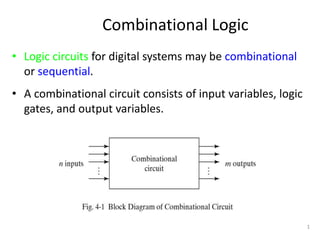
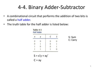
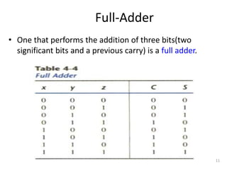
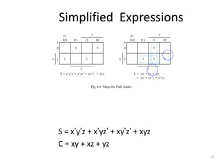
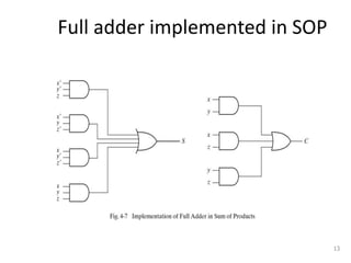
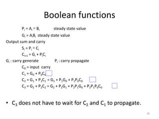
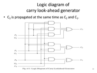
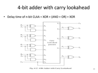
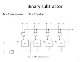
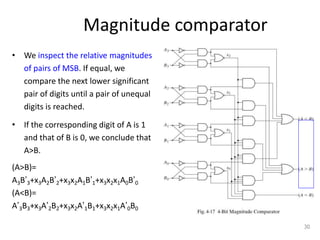
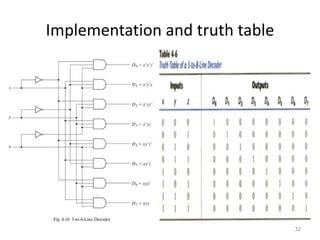
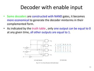
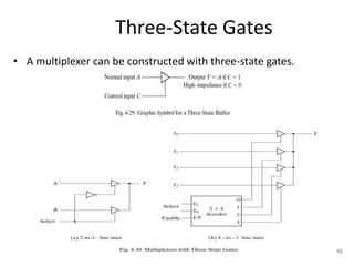
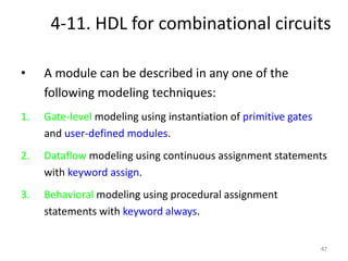
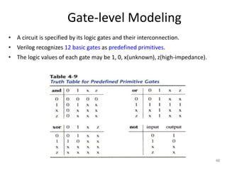
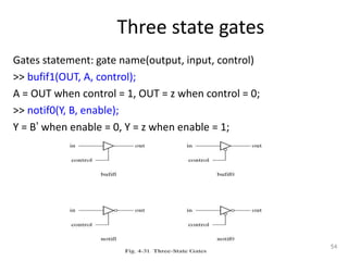
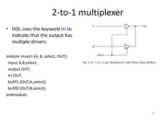
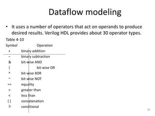
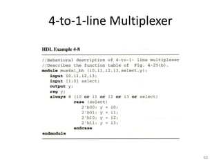
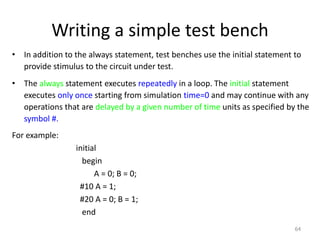
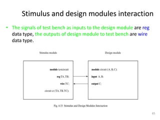
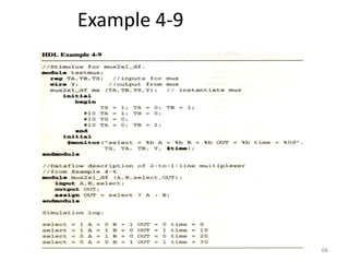
This document provides an overview of combinational logic circuits. It discusses the basic components and analysis procedures for combinational circuits. Examples are provided to demonstrate how to derive truth tables and Boolean functions from logic diagrams. Common combinational components like adders, decoders, encoders, and multiplexers are described along with their logic diagrams and implementations. HDL modeling techniques for combinational circuits using Verilog are also covered at the gate level and behavioral level.
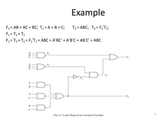

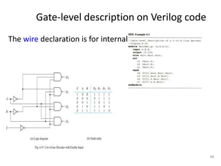
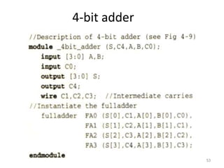
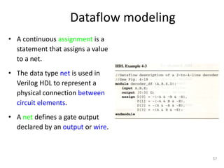
![Dataflow description of 4-bit adder
58
HDL Example 4-4
//Dataflow description of 4-bit adder
module binary_adder (A,B,Cin,SUM,Cout);
input [3:0] A,B;
input Cin;
output [3:0] SUM;
output Cout;
assign {Cout,SUM} = A + B +Cin;
endmodule](https://image.slidesharecdn.com/combinational-circuit-240221170343-39217122/85/combinational-circuits-dispositivos-ppt-58-320.jpg)


![Administracion estrategica para mantenimiento [Autoguardado].pptx](https://cdn.slidesharecdn.com/ss_thumbnails/administracionestrategicaparamantenimientoautoguardado-240113044647-54af48d7-thumbnail.jpg?width=640&height=640&fit=bounds)


