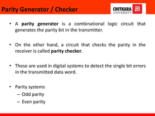
Combinational Circuits (Parity Bit Generators and Checkers)
The document discusses parity bits, which are added to transmitted data to detect errors. It describes parity generators, which create the parity bit in transmitters, and parity checkers, which check the parity in receivers. Specifically, it covers:
- Even and odd parity systems
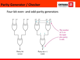
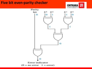
- The design of 3-bit and 4-bit even and odd parity generators and checkers using logic gates
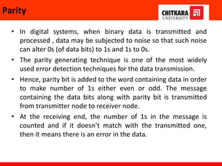
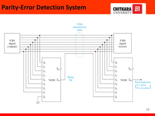
- How parity bits allow detection of single bit errors in transmitted data words
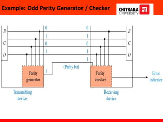
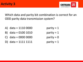
- Examples of calculating parity and troubleshooting errors in transmitted data