Downloaded 853 times
![Dr.Y.Narasimha Murthy Ph.D
yayavaram@yahoo.com
[ Normally when direction bit is 0 we will be decrementing and when direction bit is 1 we will
be incrementing].
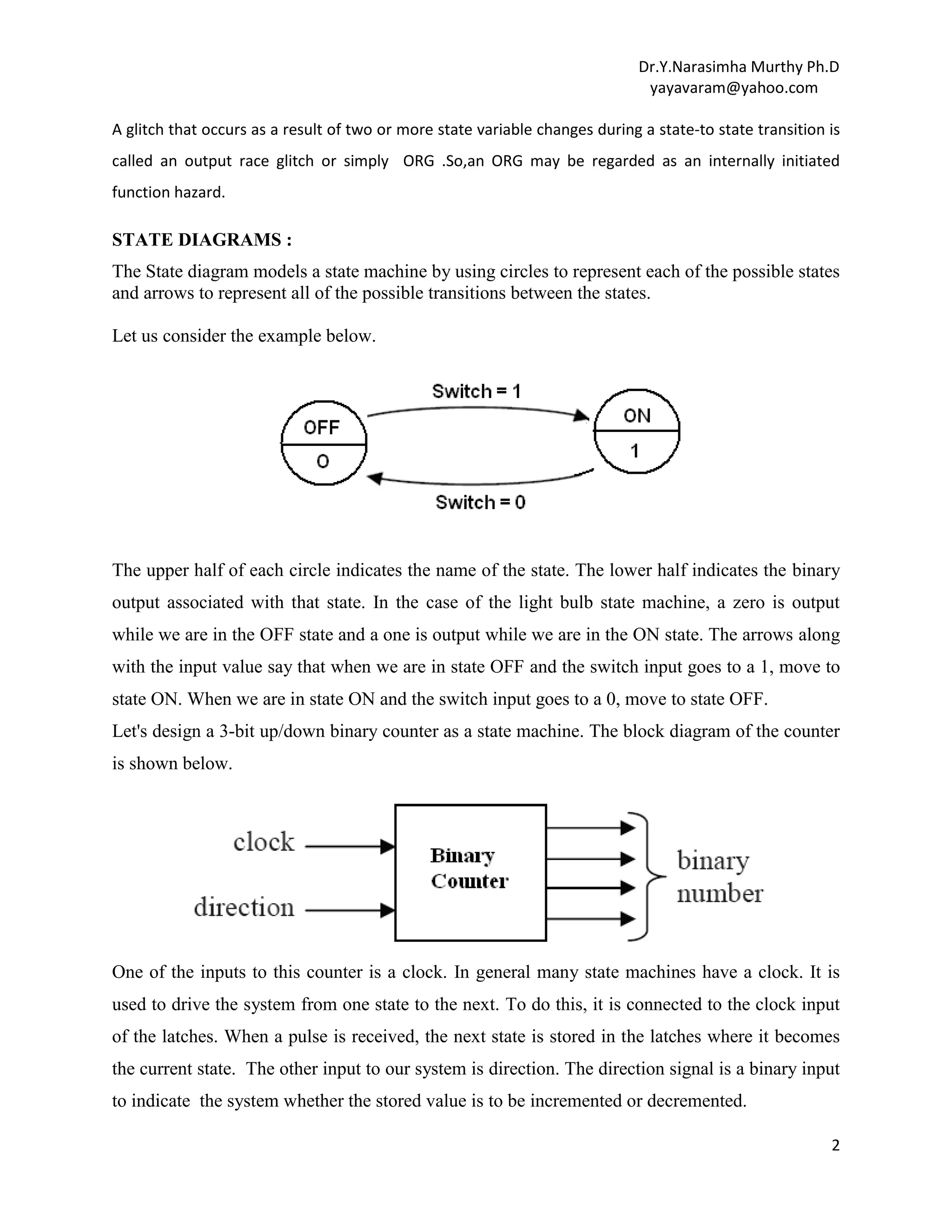
There is an additional important information that must be represented with a state diagram.
When a system first powers up, it should be initialized to a reset state. We need to indicate on the
diagram which state is defined as the initial state
A 3-bit counter has an output that is a three-bit number. Every time a clock pulse occurs, the
counter will change state to either increment or decrement the output depending on the value of
direction. For example, if direction equals one, then each clock pulse will increment the output
through the sequence 000, 001, 010, 011, 100, 101, 110, 111, 000, 001, etc. If direction equals
zero, then the output will decrement once for each clock pulse, i.e., 000, 111, 110, 101, 100,011,
010, 001, 000, 111, 001, etc.
The arrows going clockwise around the inside of the diagram represent the progression through
the states at each clock pulse when direction equals 1. The arrows going counter clockwise
around the outside of the diagram represent the progression through the states at each clock pulse
when direction equals zero.
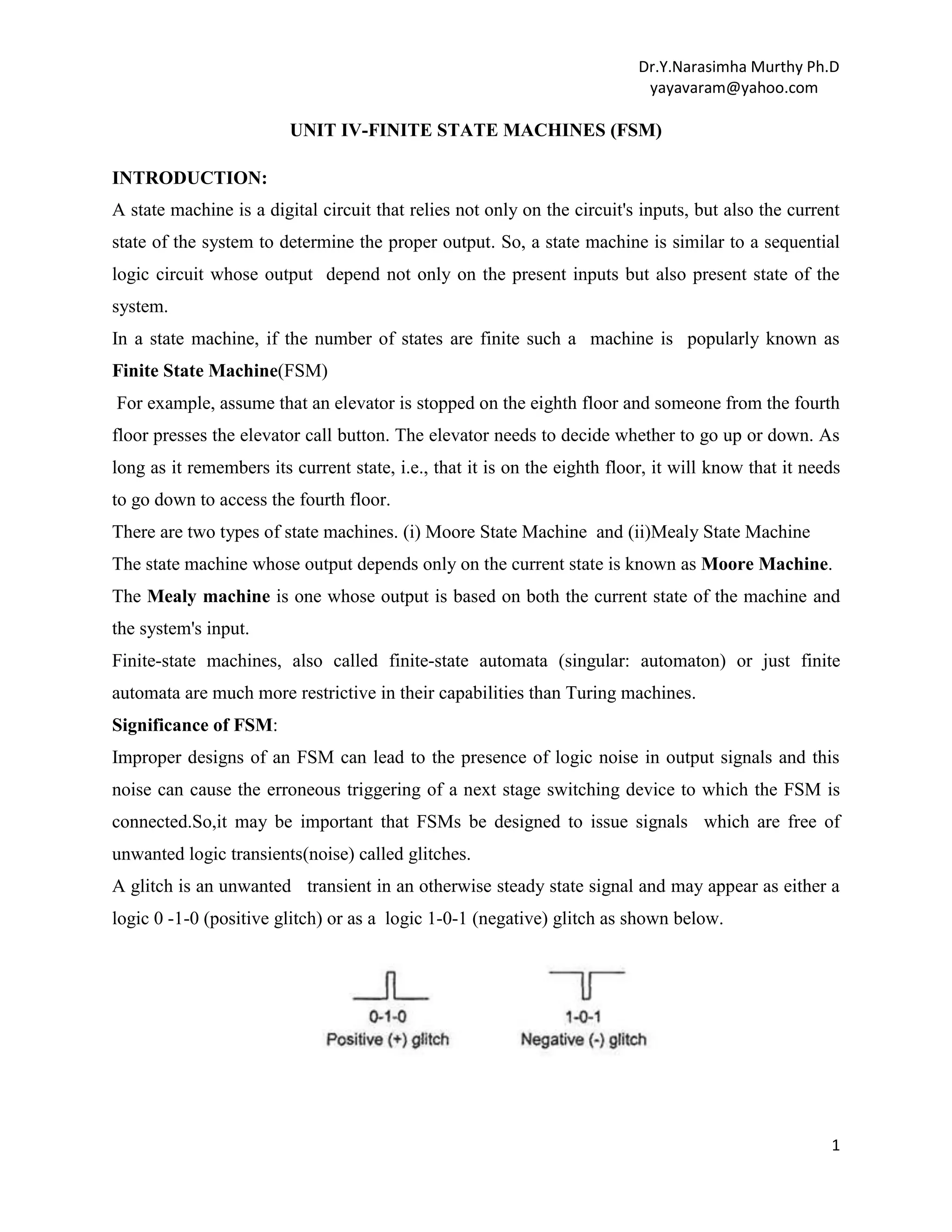
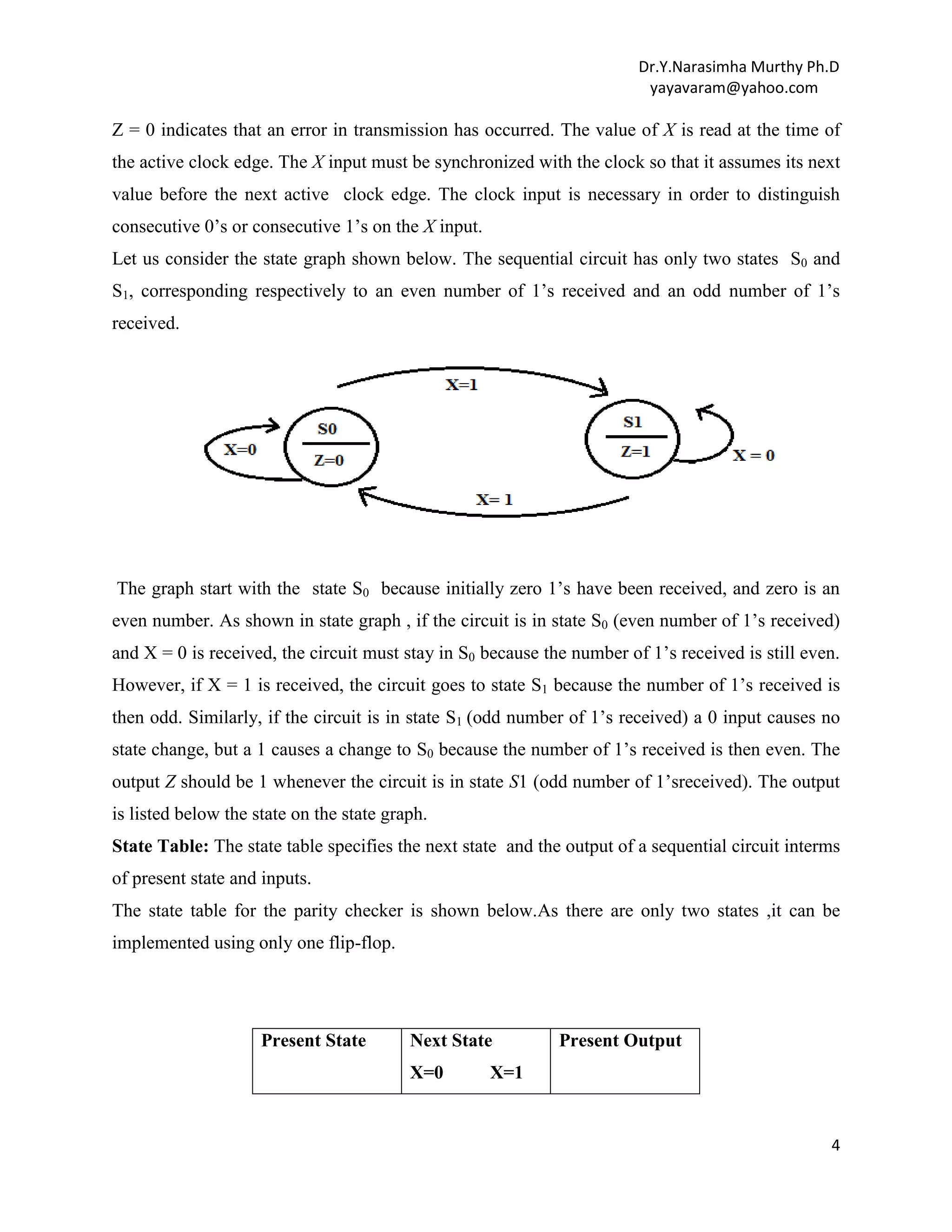
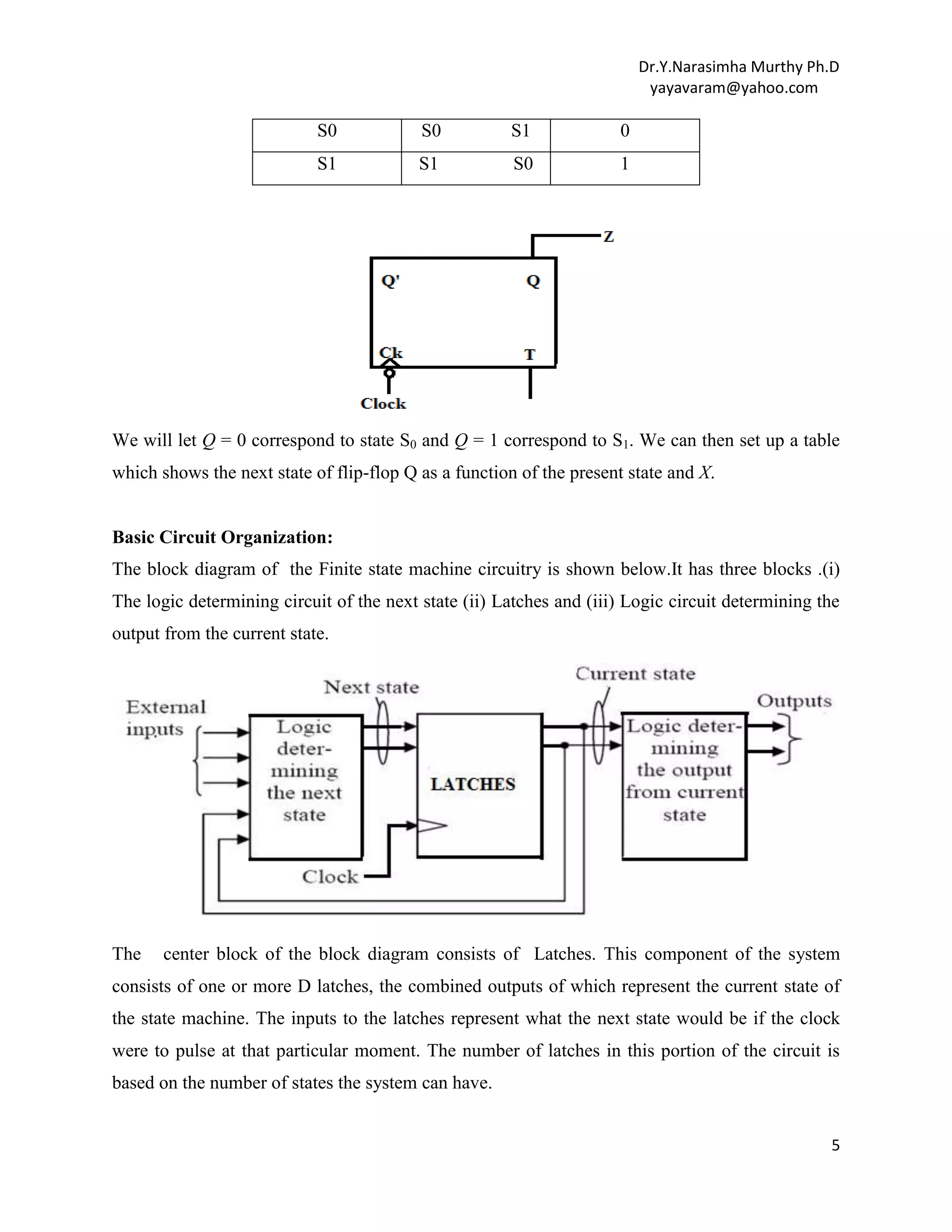
Parity Checker: The parity checker is a simple logic circuit which has one input , and one
output in addition to a clock input. This is a simple sequential circuit or FSM.
When a sequence of 0‟s and 1‟s is applied to the X input, the output of the circuit should be (Z) =
1 if the total number of 1 inputs received is odd ; that is, the output should be 1 if the input parity
is odd. Thus, if data which originally had odd parity is transmitted to the circuit, a final output of
3](https://image.slidesharecdn.com/unitiv-fsm-140101111646-phpapp01/75/UNIT-IV-FINITE-STATE-MACHINES-3-2048.jpg)

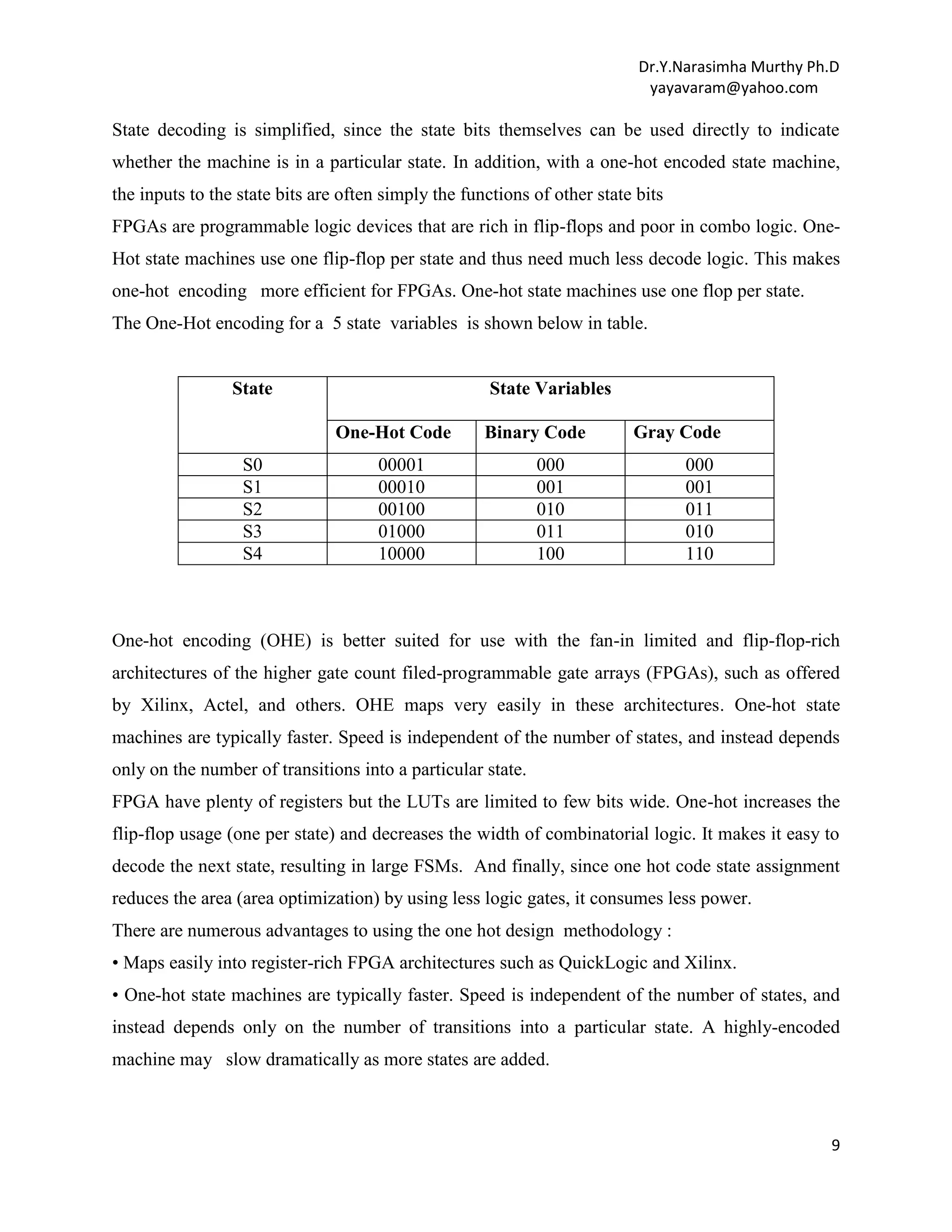


This document provides an overview of finite state machines (FSMs). It defines an FSM as a digital circuit whose output depends on both the current input and state. There are two main types of FSMs: Moore machines whose output depends only on the current state, and Mealy machines whose output depends on both the current state and input. The document discusses state diagrams, state tables, basic circuit organization including latches to represent states and combinational logic for next states and outputs. It also covers topics like state assignment methods including one-hot encoding commonly used to map FSMs onto field programmable gate arrays due to their register-rich architecture.