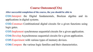
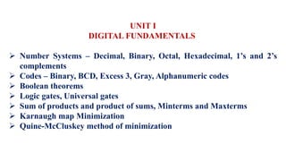
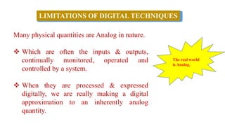
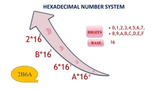
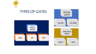
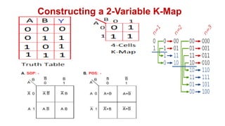
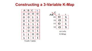
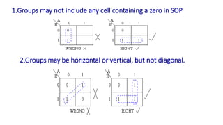
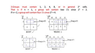
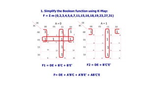
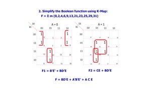
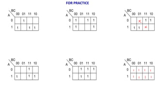
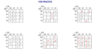
The document outlines the syllabus and course objectives for the Digital Electronics course at R.M.K. College of Engineering & Technology, focusing on digital fundamentals, combinational and sequential circuit design, semiconductor memory, and logic gate technology. It includes topics on various number systems, circuit design principles, and practical applications of digital systems. The course aims to equip students with skills to interpret digital fundamentals and construct combinational and sequential digital circuits, as well as compare different logic families.


![MINIMIZATION OF BOOLEAN EXPRESSIONS
EXAMPLE 1: [(A + B’) (C + D’)]’
= (A + B’)’ + (C + D’)’
= A’ B’’ + C’D’’
= A’B + C’D
EXAMPLE 2: REDUCE A (A + B)
=A (A + B) = AA + AB
= A (1 + B) [1 + B = 1]
= A](https://image.slidesharecdn.com/digitalelectronicsec8392unit-1ppt-seshavidhyas-210908134810/85/Digital-electronics-EC8392-unit-1-Sesha-Vidhya-S-ASP-ECE-RMKCET-93-320.jpg)
![EXAMPLE 3 : [(AB)’ + A’ + AB]’
= (AB)’’ · A’’ · (AB)’
= ABA (A’ + B’)
= ABA’ + ABB’
= 0
EXAMPLE 4 : Y = (A + B) (A + C’) (B' + C’)
= (AA' + AC +A'B +BC) (B' + C') [A.A' = 0]
= (AC + A'B + BC) (B' + C’)
= AB'C + ACC' + A'BB' + A'BC' + BB'C + BCC’
= AB'C + A'BC'](https://image.slidesharecdn.com/digitalelectronicsec8392unit-1ppt-seshavidhyas-210908134810/85/Digital-electronics-EC8392-unit-1-Sesha-Vidhya-S-ASP-ECE-RMKCET-94-320.jpg)
![EXAMPLE 5 : SHOW THAT (X + Y' + XY) (X + Y') (X'Y) = 0
(X + Y' + XY)(X + Y')(X'Y)
= (X + Y' + X) (X + Y’) (X' + Y) [A + A'B = A + B]
= (X + Y’) (X + Y’) (X’Y) [A + A = 1]
= (X + Y’) (X’Y) [A.A = 1]
= X.X' + Y'.X'.Y = 0 [A.A' = 0]
EXAMPLE 6 : PROVE THAT ABC + ABC' + AB'C + A'BC = AB + AC + BC
ABC + ABC' + AB'C + A'BC
=AB(C + C') + AB'C + A'BC
=AB + AB'C + A'BC =A(B + B'C) + A'BC
=A(B + C) + A'BC
=AB + AC + A'BC
=B(A + C) + AC
=AB + BC + AC](https://image.slidesharecdn.com/digitalelectronicsec8392unit-1ppt-seshavidhyas-210908134810/85/Digital-electronics-EC8392-unit-1-Sesha-Vidhya-S-ASP-ECE-RMKCET-95-320.jpg)


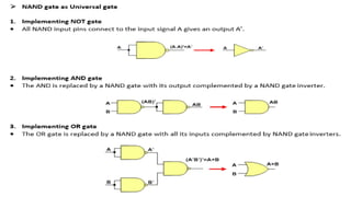
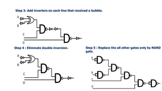
![Realize the following Boolean Expression using NAND Gate:
F = [(A+B)C]’.D
NAND Gate Implementation
Step 1: Draw the logic diagram using basic gates.
Step 2 : Add bubbles at the output of the AND Gate and the input of the OR Gate.](https://image.slidesharecdn.com/digitalelectronicsec8392unit-1ppt-seshavidhyas-210908134810/85/Digital-electronics-EC8392-unit-1-Sesha-Vidhya-S-ASP-ECE-RMKCET-130-320.jpg)
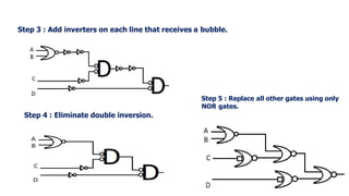
![NOR Gate Implementation
Implement the following Boolean Expression using NOR Gate
only : F = [(A+B)C]’.D
Step 1: Draw the logic diagram using basic gates.
Step 2: Add bubbles at the output of OR gate
and input of AND gate.](https://image.slidesharecdn.com/digitalelectronicsec8392unit-1ppt-seshavidhyas-210908134810/85/Digital-electronics-EC8392-unit-1-Sesha-Vidhya-S-ASP-ECE-RMKCET-132-320.jpg)