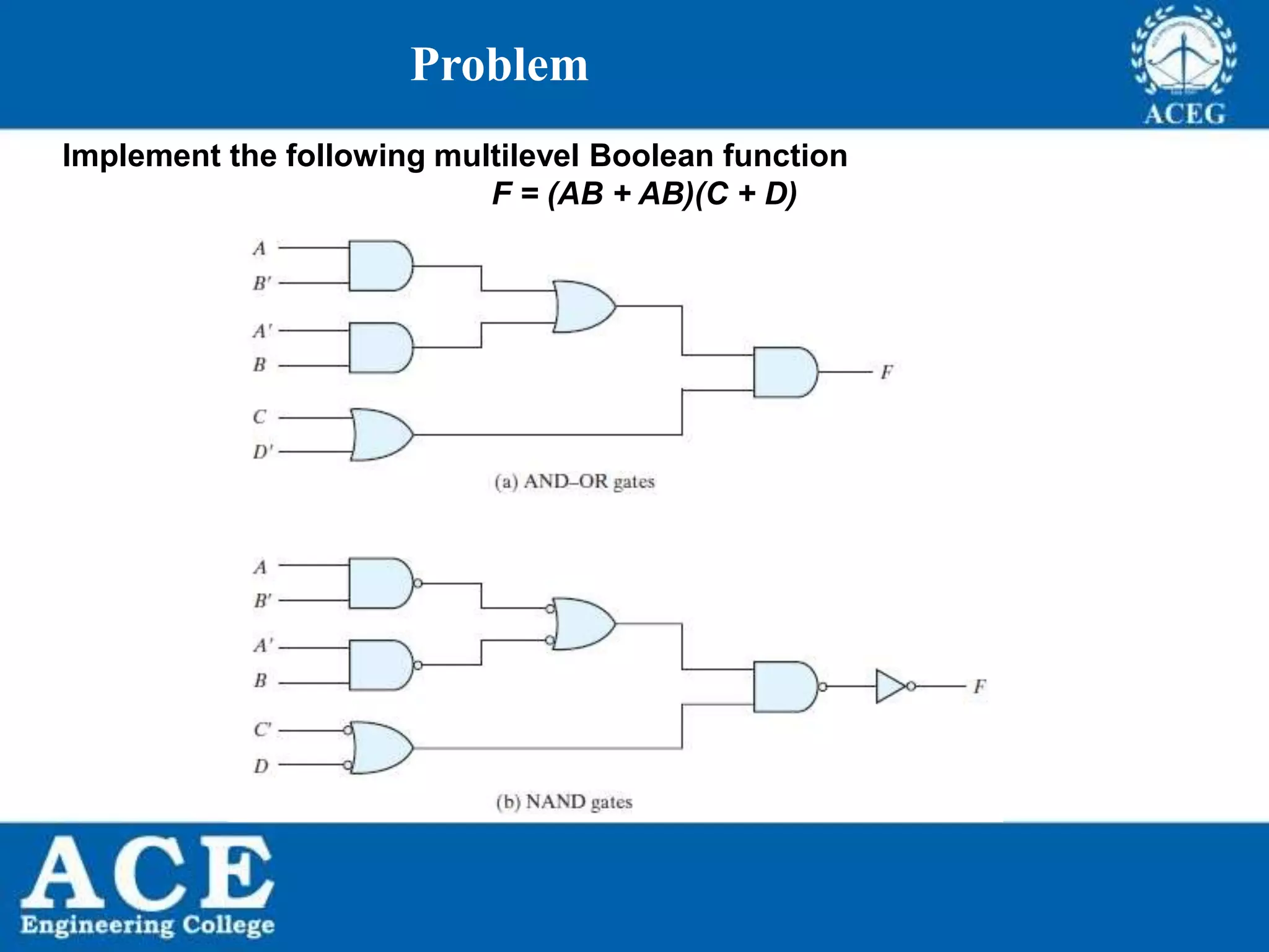
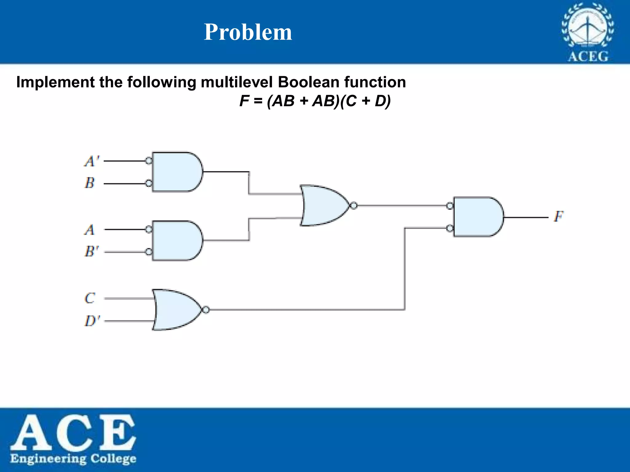
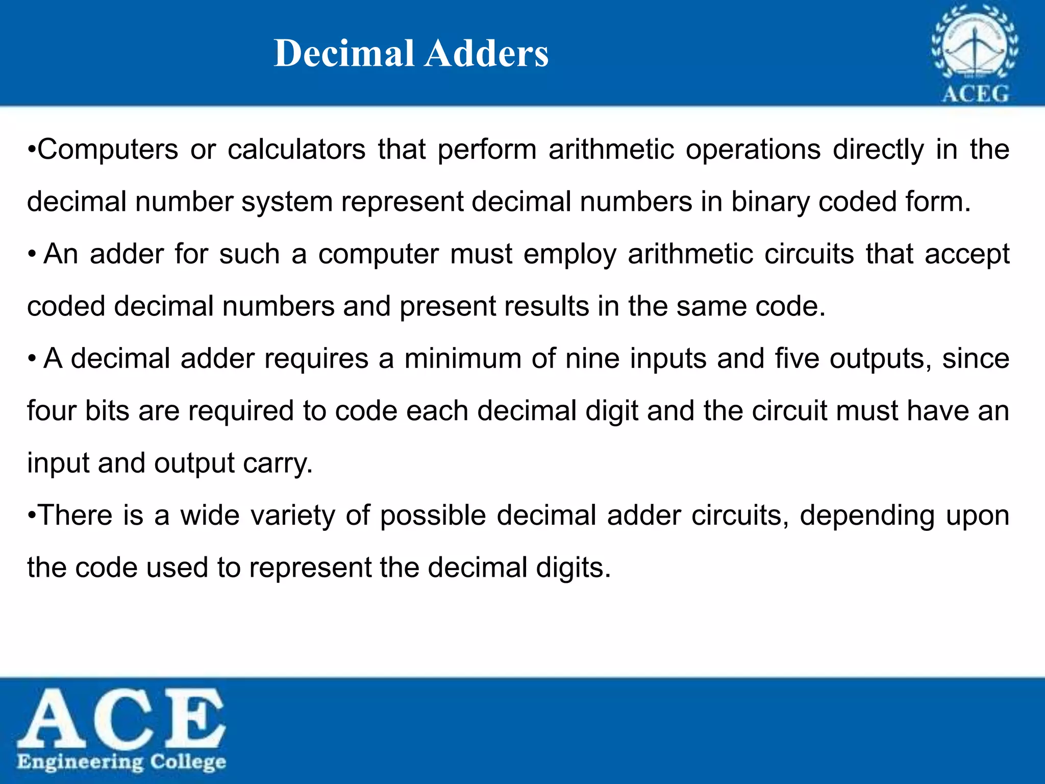
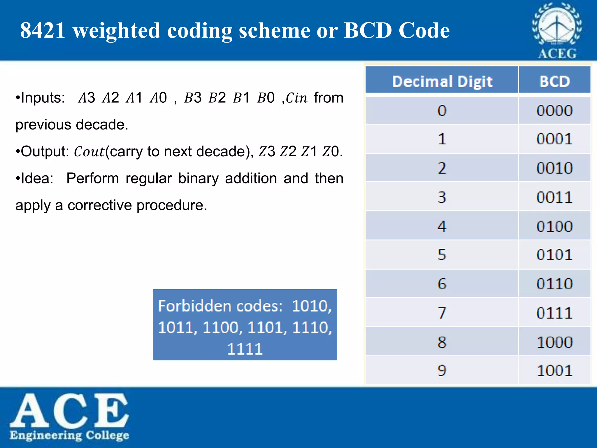
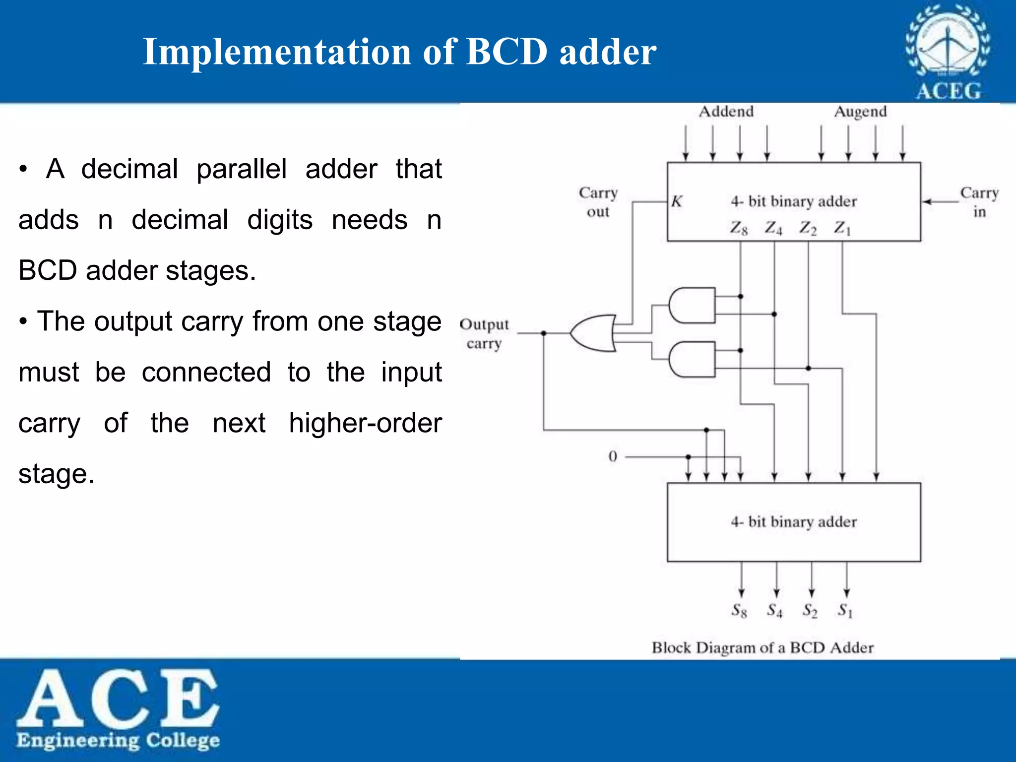
Downloaded 108 times


![P.KIRAN KUMAR,ECE DEPARTMENT 87
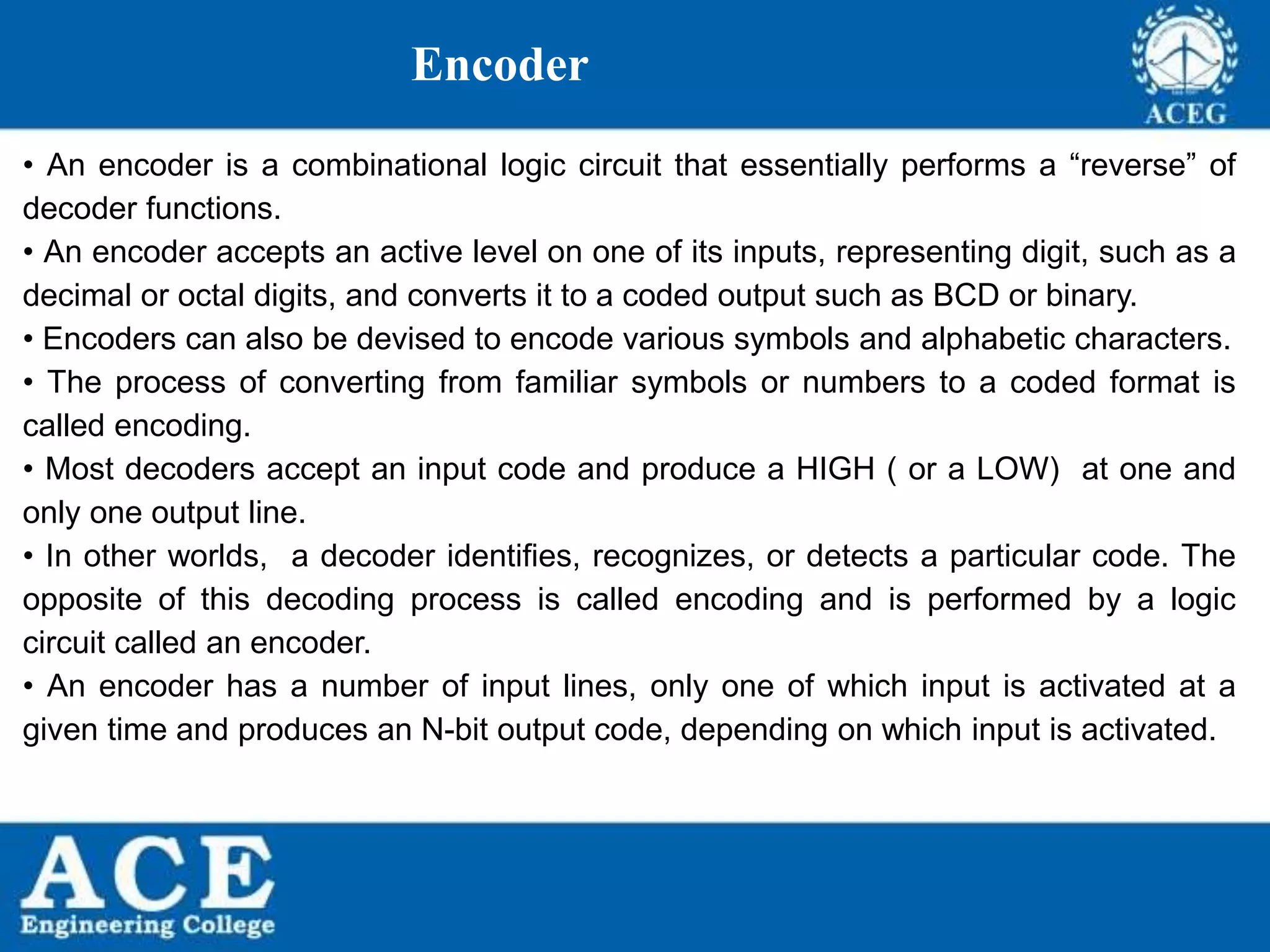
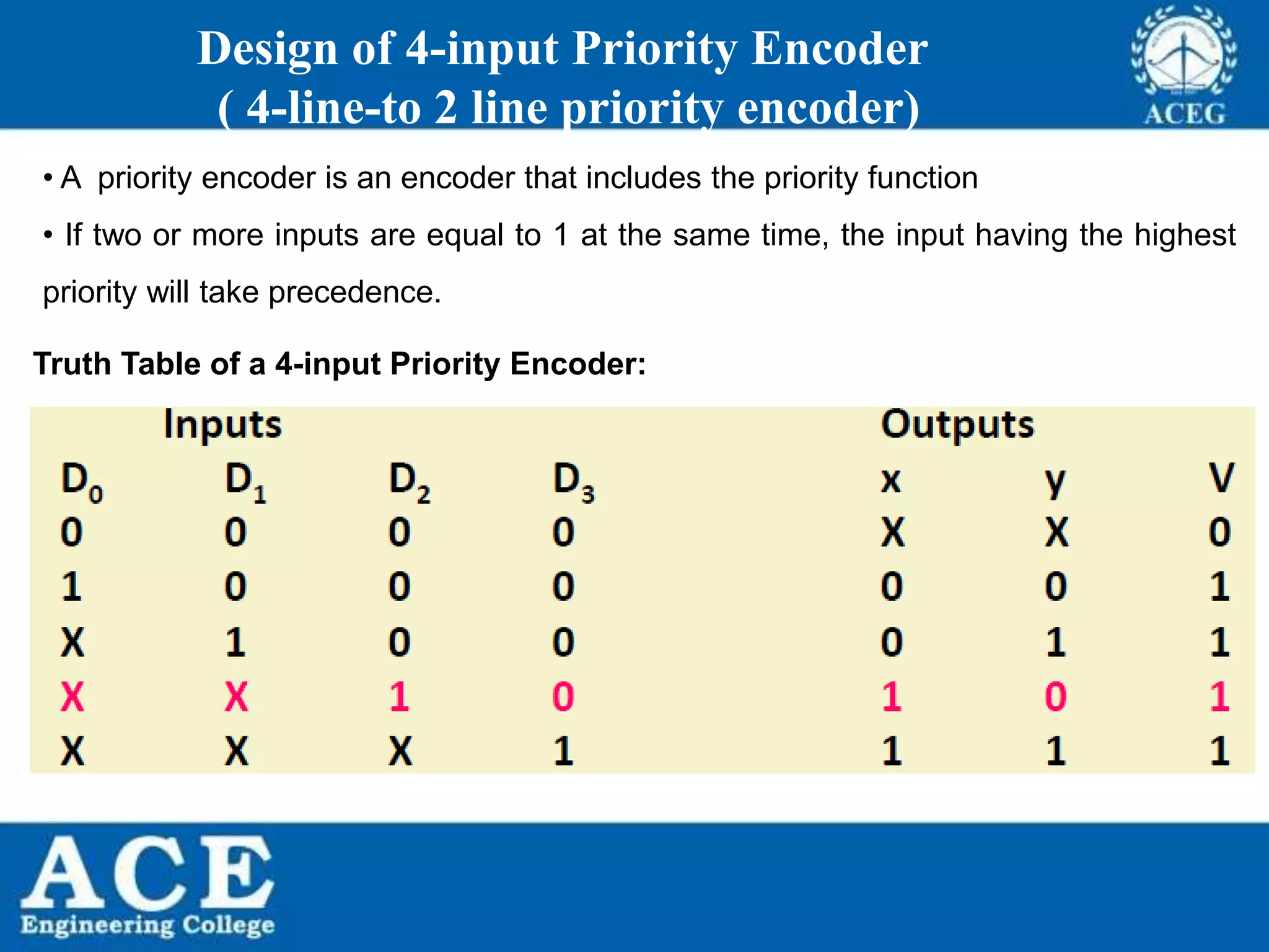
Encoder
General encoder diagram Logic circuit for octal-to binary encoder
[8-line-3-line ]](https://image.slidesharecdn.com/aedeunit-4-191121144853/75/ANALOG-AND-DIGITAL-ELECTRONICS-unit-4-87-2048.jpg)
![P.KIRAN KUMAR,ECE DEPARTMENT 88
Encoder
Truth table for octal-to binary encoder [8-line-3-line ]
A low at any single input will produce the output binary code corresponding to that
input. For instance, a low at A3’ will produce O2=0, O1=1 and O0=1, which is binary
code for 3. Ao’ is not connected to the logic gates because the encoder outputs
always be normally at 000 when none of the inputs is LOW](https://image.slidesharecdn.com/aedeunit-4-191121144853/75/ANALOG-AND-DIGITAL-ELECTRONICS-unit-4-88-2048.jpg)


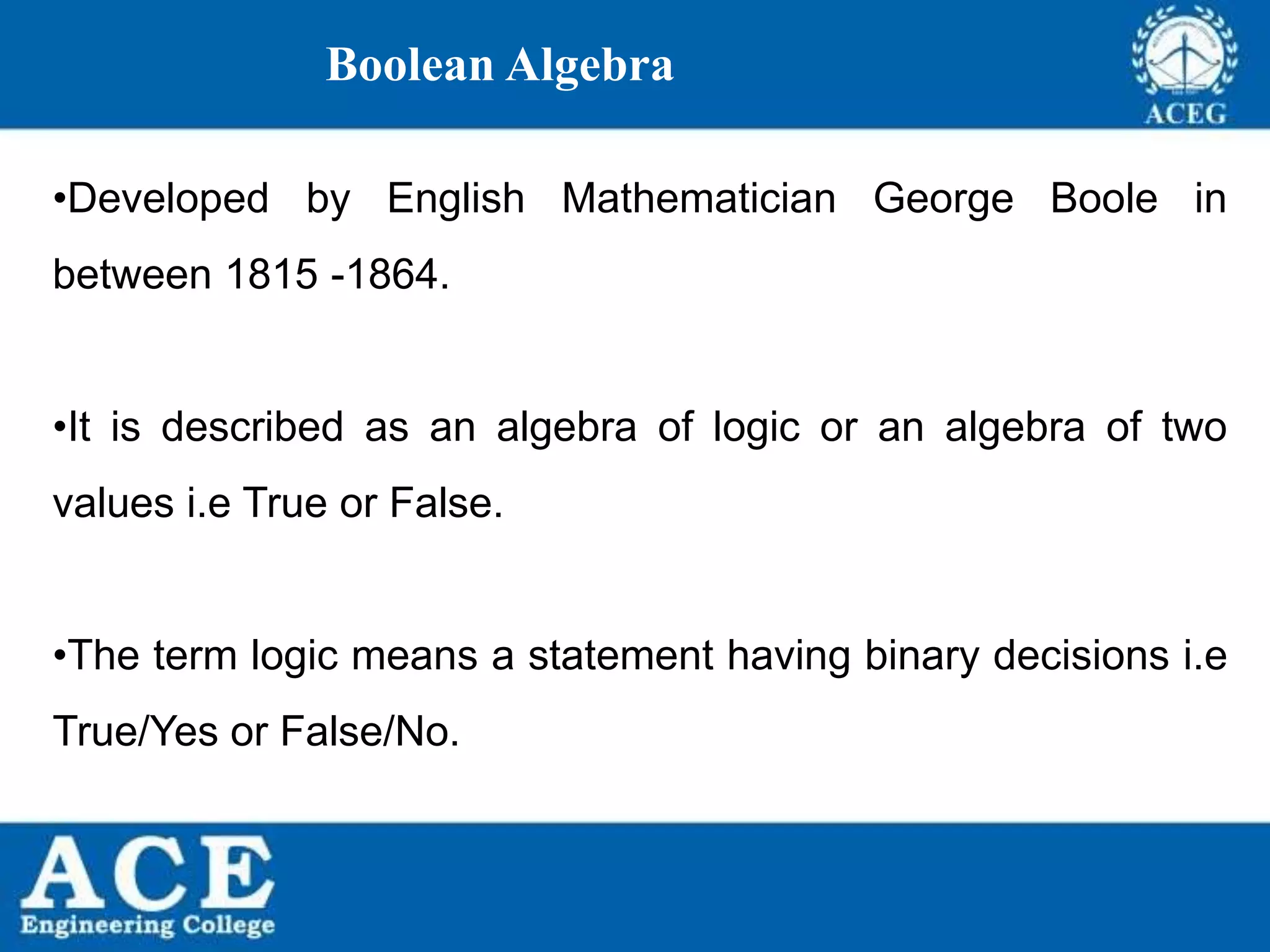
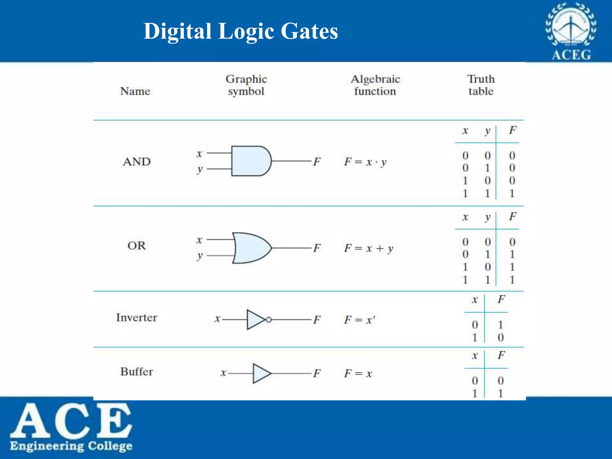
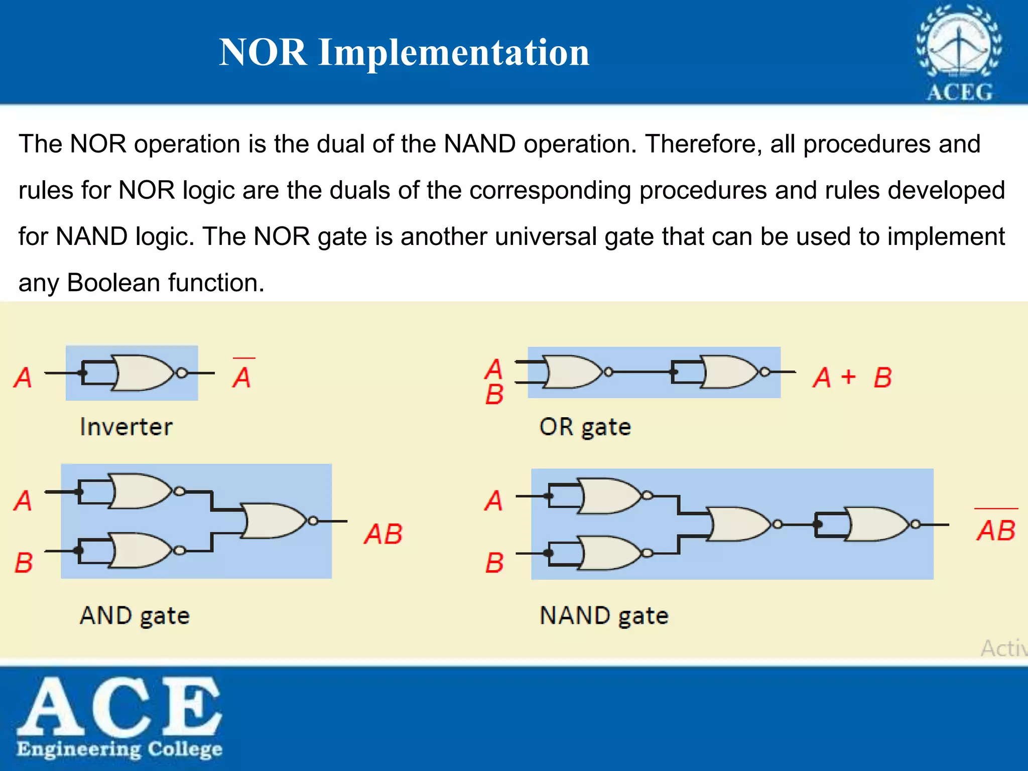
The document provides an overview of Boolean algebra, detailing its development by George Boole and its applications in digital electronics. It covers logical operations, fundamental operators, the formation of Boolean functions, canonical forms, and the minimization of Boolean expressions using methods such as Karnaugh maps. Additionally, it discusses the implementation of Boolean functions using NAND and NOR gates, along with the designs of adders and multipliers in digital circuits.


![SEQUENTIAL CIRCUITS [FLIP FLOPS AND LATCHES]](https://cdn.slidesharecdn.com/ss_thumbnails/sequentialcircuits-211203044039-thumbnail.jpg?width=640&height=640&fit=bounds)