Chapter 3: MOSFET
Introduction
Classifications
JFET
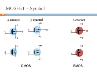
D-MOSFET (Depletion MOS, DFET…)
MOSFET (Enhancement E-MOSFET/ E-FET)
DC biasing
AC Analysis (Small signal analysis)
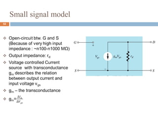
Equivalent small signal circuit
2
3.
FET Introduction
Highinput impedance, nMΩ-n100MΩ
Controlled by voltage (≠ BJT)
Low power consumption
Low noise, suitable for small signal
Low impact of temperature
Using as switch for low power application
Small size and adapt for integrated circuit
3
4.
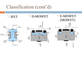
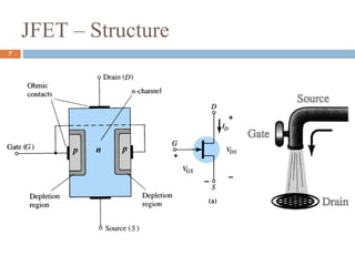
Classification
JFET-Junction FieldEffect Transistor
🞑 N and P channels
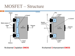
MOSFET-Metal Oxide Semiconductor FET
🞑 Depletion MOS
N and P channels
🞑 Enhancement MOS
N and P channels
4
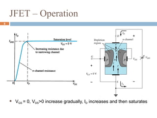
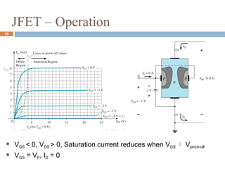
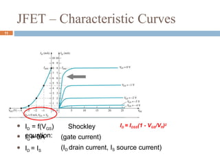
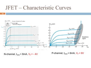
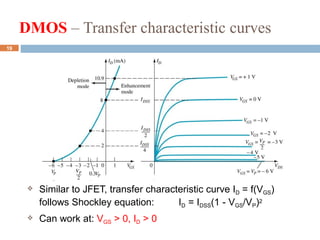
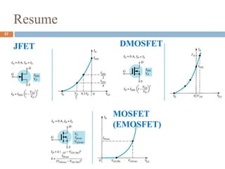
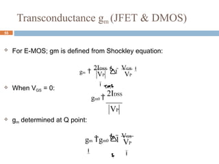
DMOS – Transfercharacteristic curves
Similar to JFET, transfer characteristic curve ID = f(VGS)
follows Shockley equation: ID = IDSS(1 - VGS/VP)2
Can work at: VGS > 0, ID > 0
19
20.
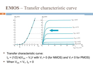
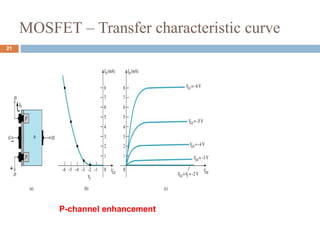
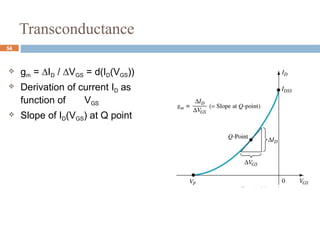
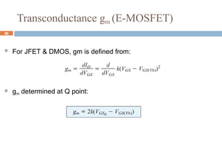
EMOS – Transfercharacteristic curve
Transfer characteristic curve:
ID = (1/2) k(VGS – VT)2 with VT > 0 (for NMOS) and VT< 0 for PMOS)
When VGS < VT, ID = 0
20
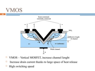
VMOS
VMOS –Vertical MOSFET, increase channel lenght
Increase drain current thanks to large space of heat release
High switching speed
25
26.
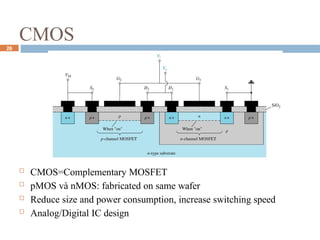
CMOS
CMOS=Complementary MOSFET
pMOS và nMOS: fabricated on same wafer
Reduce size and power consumption, increase switching speed
Analog/Digital IC design
26
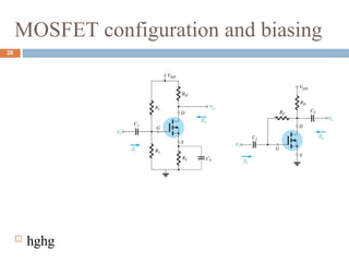
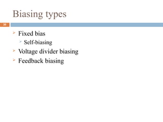
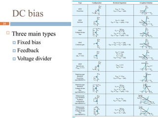
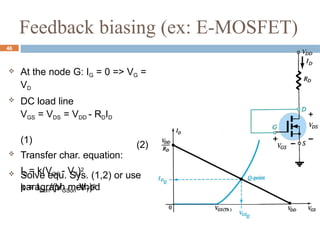
DC bias
Threemain types
🞑 Fixed bias
🞑 Feedback
🞑 Voltage divider
31
32.
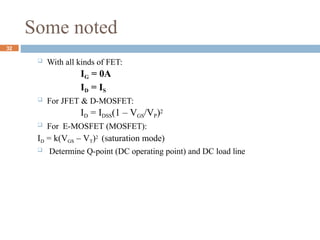
Some noted
Withall kinds of FET:
IG = 0A
ID = IS
For JFET & D-MOSFET:
ID = IDSS(1 – VGS/VP)2
For E-MOSFET (MOSFET):
ID = k(VGS – VT)2 (saturation mode)
Determine Q-point (DC operating point) and DC load line
32
33.
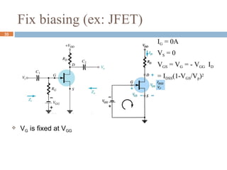
Fix biasing (ex:JFET)
IG = 0A
VS = 0
VGS = VG = - VGG ID
= IDSS(1-VGS/Vp)2
VG is fixed at VGG
33
34.
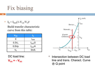
Fix biasing
ID= IDSS(1-VGS/VP)2
Build transfer characteristic
curve from this table:
VGS ID
0 IDSS
0.3VP IDSS/2
0.5Vp IDSS/4
VP 0mA
DC load line:
VGS = - VGG
Intersection between DC load
line and trans. Charact. Curve
Q point
34
35.
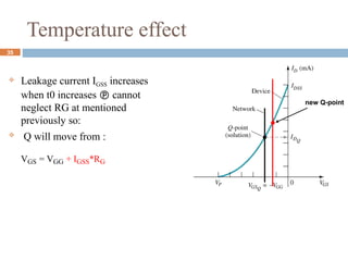
Temperature effect
Leakagecurrent IGSS increases
when t0 increases cannot
neglect RG at mentioned
previously so:
Q will move from :
VGS = VGG + IGSS*RG
new Q-point
35
36.
new Q-point
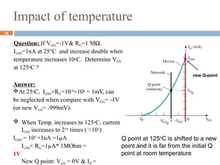
Answer:
At 25oC,IGSS×RG=10-9×106 = 1mV, can
be neglected when compare with VGG= -1V
(or new VGS= -999mV).
Q point at 1250C is shifted to a new
point and it is far from the initial Q
point at room temperature
36
Question: If VGG=-1V& RG=1 MΩ.
IGSS=1nA at 25°C and increase double when
temperature increases 10oC. Determine VGS
at 125oC ?
When Temp. increases to 125oC, current
IGSS increases to 210 times ( ≈103)
IGSS = 103 ×1nA =1µA
IGSS× RG=1µA* 1MOhm =
1V
New Q point: VGS = 0V & ID =
Impact of temperature
37.
For E-MOSFET:
ID =½*k(VGS-VT)2
k=IDon/(VGSon-VT)2 = μCoxW/L
Where μ is mobility (m2/V.s)
Cox is oxide capacitance ~
ε0εox/tox
W, L are width and length dimension of
43
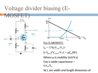
Voltage divider biasing (E-
MOSFET)
38.
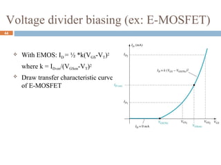
With EMOS:ID = ½ *k(VGS-VT)2
where k = ID-on/(VGSon-VT)2
Draw transfer characteristic curve
of E-MOSFET
44
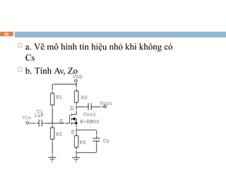
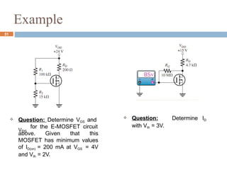
Voltage divider biasing (ex: E-MOSFET)
Example
51
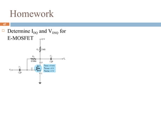
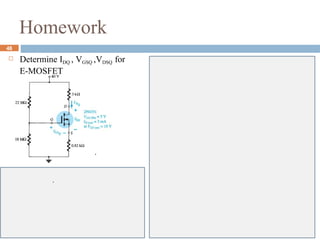
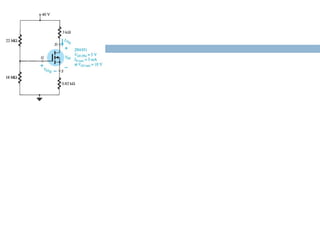
Question: DetermineVGS and
VDS
for the E-MOSFET circuit
above. Given that this
MOSFET has minimum values
of ID(on) = 200 mA at VGS = 4V
and Vth = 2V.
Question: Determine ID
with Vth = 3V.
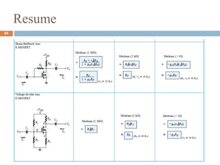
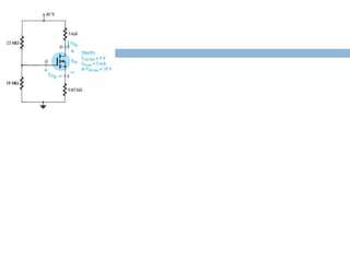
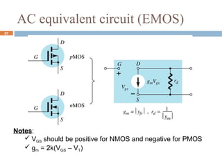
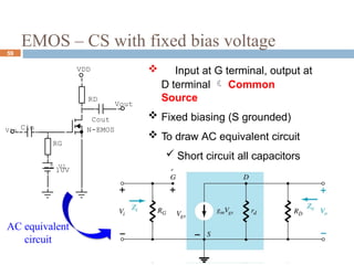
EMOS – CSwith fixed bias voltage
59
Vout
Vin Cin
+ V1
10V
VDD
RG
RD
Cout
N-EMOS
Input at G terminal, output at
D terminal Common
Source
Fixed biasing (S grounded)
To draw AC equivalent circuit
Short circuit all capacitors
Short circuit power supply
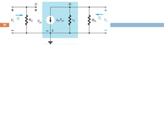
AC equivalent
circuit
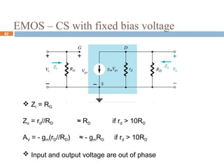
Zi =RG
Zo = rd//RD ≈ RD if rd > 10RD
AV = - gm(rD//RD) ≈ - gmRD if rd > 10RD
Input and output voltage are out of phase
EMOS – CS with fixed bias voltage
62
57.
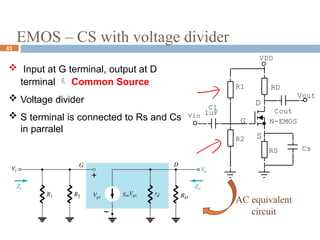
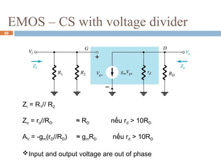
EMOS – CSwith voltage divider
63
Input at G terminal, output at D
terminal Common Source
Voltage divider
S terminal is connected to Rs and Cs
in parralel
G
D
S
R1
Cs
RS
Cout
Vout
C1
Vin 1uF
VDD
R2
RD
N-EMOS
AC equivalent
circuit
EMOS – CSwith voltage divider
Zi = R1// R2
Zo = rd//RD ≈ RD nếu rd > 10RD
AV = -gm(rD//RD) ≈ gmRD nếu rd > 10RD
Input and output voltage are out of phase
66
61.
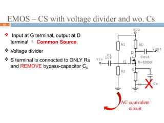
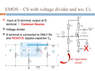
EMOS – CSwith voltage divider and wo. Cs
67
Input at G terminal, output at D
terminal Common Source
Voltage divider
S terminal is connected to ONLY Rs
and REMOVE bypass-capacitor CS
G
D
S
R1
Cout
Vout
C1
Vin 1uF
VDD
R2
RD
N-EMOS
RS
XCs
AC equivalent
circuit
EMOS – CSwith voltage divider and wo. Cs
70
Input at G terminal, output at D
terminal Common Source
Voltage divider
S terminal is connected to ONLY Rs
and REMOVE bypass-capacitor CS
G
D
S
R1
Cout
Vout
C1
Vin 1uF
VDD
R2
RD
N-EMOS
RS
XCs
AC equivalent
circuit
EMOS – CSwith voltage divider and wo. Cs
Zi = RG
Zo =
(or R1//R2)
AV = -gmRD/[1+gmRS+(RD+RS)/rd]
Input and output voltage are out of phase
73
68.
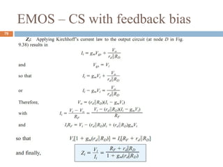
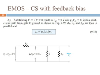
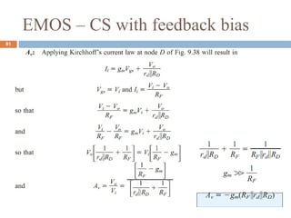
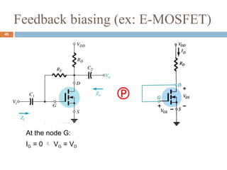
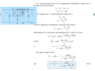
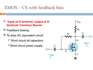
EMOS – CSwith feedback bias
Input at G terminal, output at D
terminal: Common Source
Feedback biasing
To draw AC equivalent circuit
Short circuit all capacitors
Short circuit power supply
74
69.
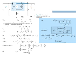
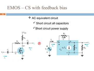
EMOS – CSwith feedback bias
75
AC equivalent circuit
Short circuit all capacitors
Short circuit power supply
EMOS – CSwith feedback bias
Zi = (RF+rd//RD)/[1+gm(rd//RD)]
≈ RF/(1+gmRD) with rd >10RD, RF>>rd//RD
Zo = RF//rd//RD ≈ RD with rd >10RD, RF>>rd//RD
AV = gm RF//rd//RD ≈ gmRD with rd >10RD,
RF>>rd//RD
Output and input voltage are out of phase
78
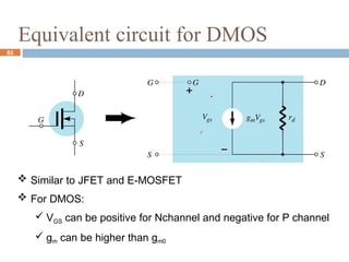
Equivalent circuit forDMOS
Similar to JFET and E-MOSFET
For DMOS:
VGS can be positive for Nchannel and negative for P channel
gm can be higher than gm0
83


![EMOS – CS with voltage divider and wo. Cs
Zi = RG
Zo =
(or R1//R2)
AV = -gmRD/[1+gmRS+(RD+RS)/rd]
Input and output voltage are out of phase
73](https://image.slidesharecdn.com/20241chapter2fet-250315141930-f6fceb91/85/20241_Chapter-2-_FEergergergergedfgdfT-pptx-67-320.jpg)


![EMOS – CS with feedback bias
Zi = (RF+rd//RD)/[1+gm(rd//RD)]
≈ RF/(1+gmRD) with rd >10RD, RF>>rd//RD
Zo = RF//rd//RD ≈ RD with rd >10RD, RF>>rd//RD
AV = gm RF//rd//RD ≈ gmRD with rd >10RD,
RF>>rd//RD
Output and input voltage are out of phase
78](https://image.slidesharecdn.com/20241chapter2fet-250315141930-f6fceb91/85/20241_Chapter-2-_FEergergergergedfgdfT-pptx-72-320.jpg)