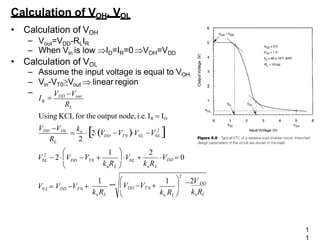
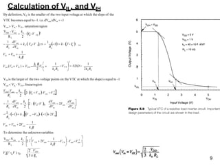
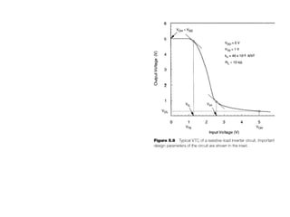
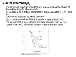
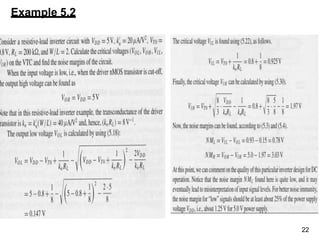
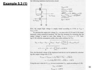
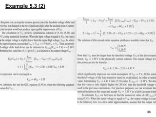
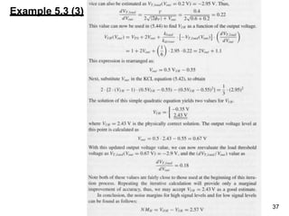
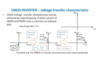
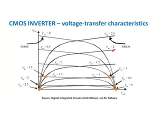
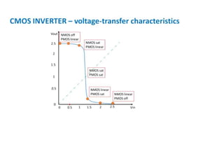
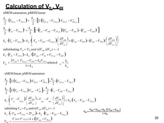
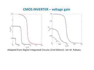
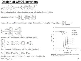
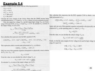
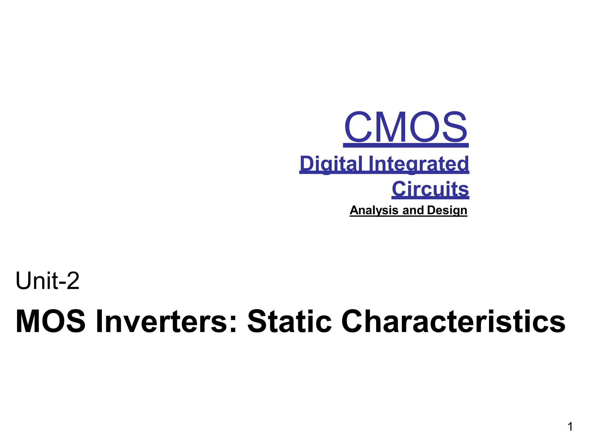
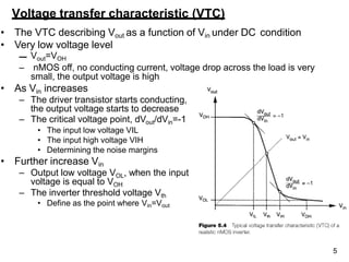
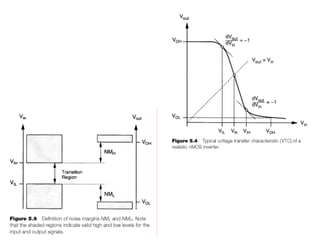
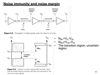
1) The document discusses the static characteristics of MOS inverters, including their voltage transfer characteristic (VTC), noise margins, and calculations of key voltages like VOH, VOL, VIL and VIH.
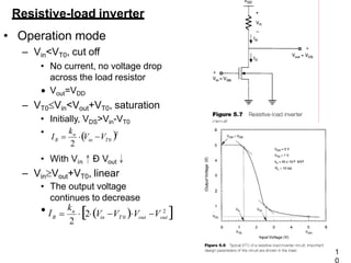
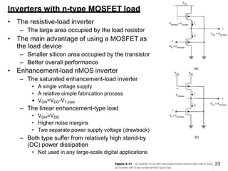
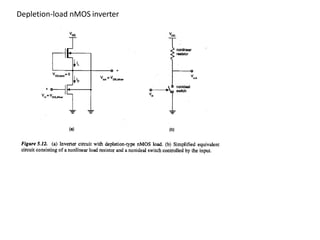
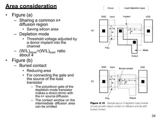
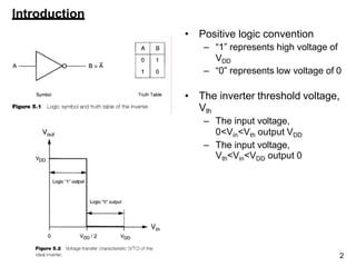
2) It describes the general circuit structure of an nMOS inverter using an nMOS transistor as the driver and either a resistor or depletion-mode nMOS as the load.
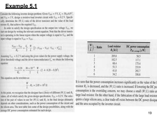
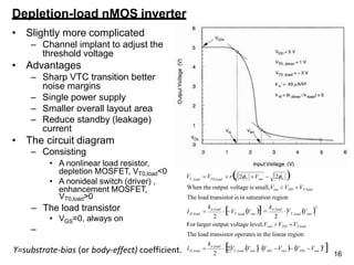
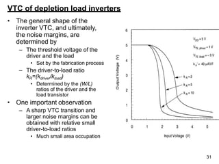
3) Key parameters that determine the VTC shape include knRL (the product of transconductance and load resistance) and the load used - resistive or depletion-mode nMOS, with the latter providing better noise margins and smaller area.


![9
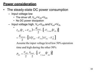
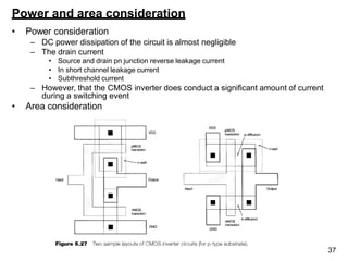
Power and area consideration
• The DC power dissipation
– The product of its power supply voltage and the
amount of current down from the power supply during
steady state or in standby mode
– PDC=VDDIDC=(VDD/2)[IDC(Vin=low)+IDC(Vin=high)]
– In deep submicron technologies
• Subthreshold current is high therefore more power
consumption
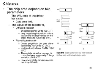
• The chip area
– To reduce the area of the MOS transistor
• The gate area of the MOS transistor
• The product of W and L](https://image.slidesharecdn.com/mosinvertersstaticcharacteristics-240306174106-97634391/85/MOS-Inverters-Static-Characteristics-pptx-9-320.jpg)