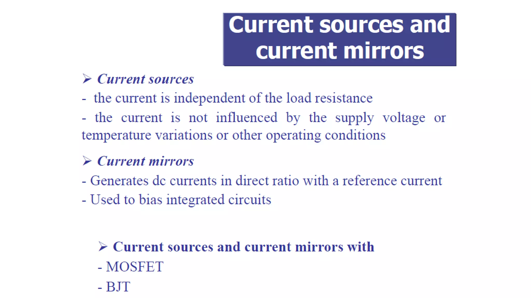
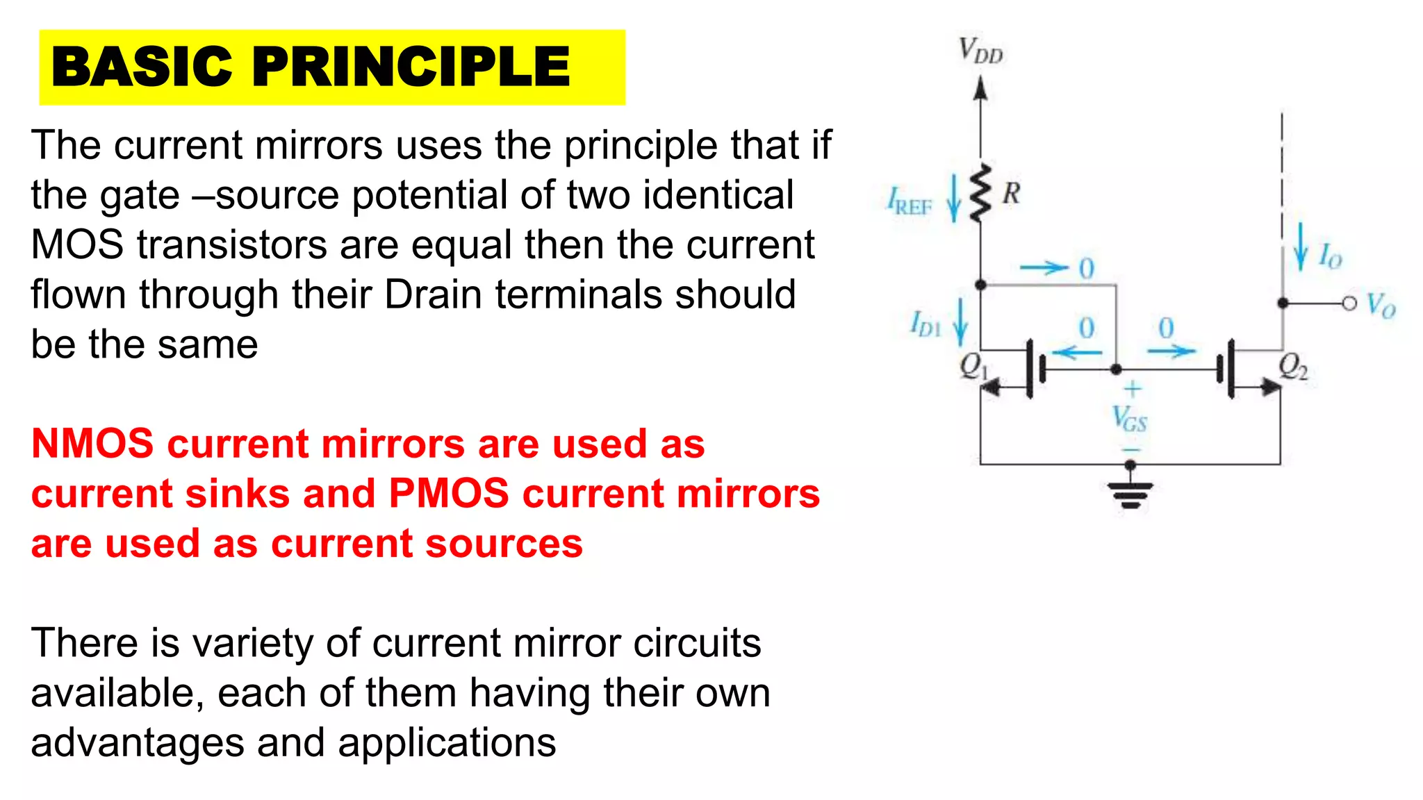
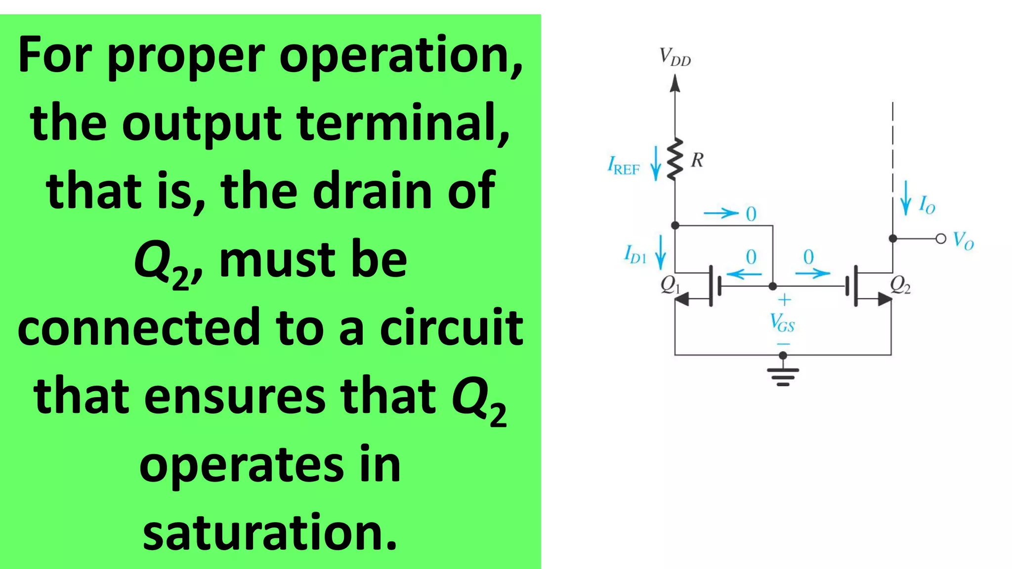
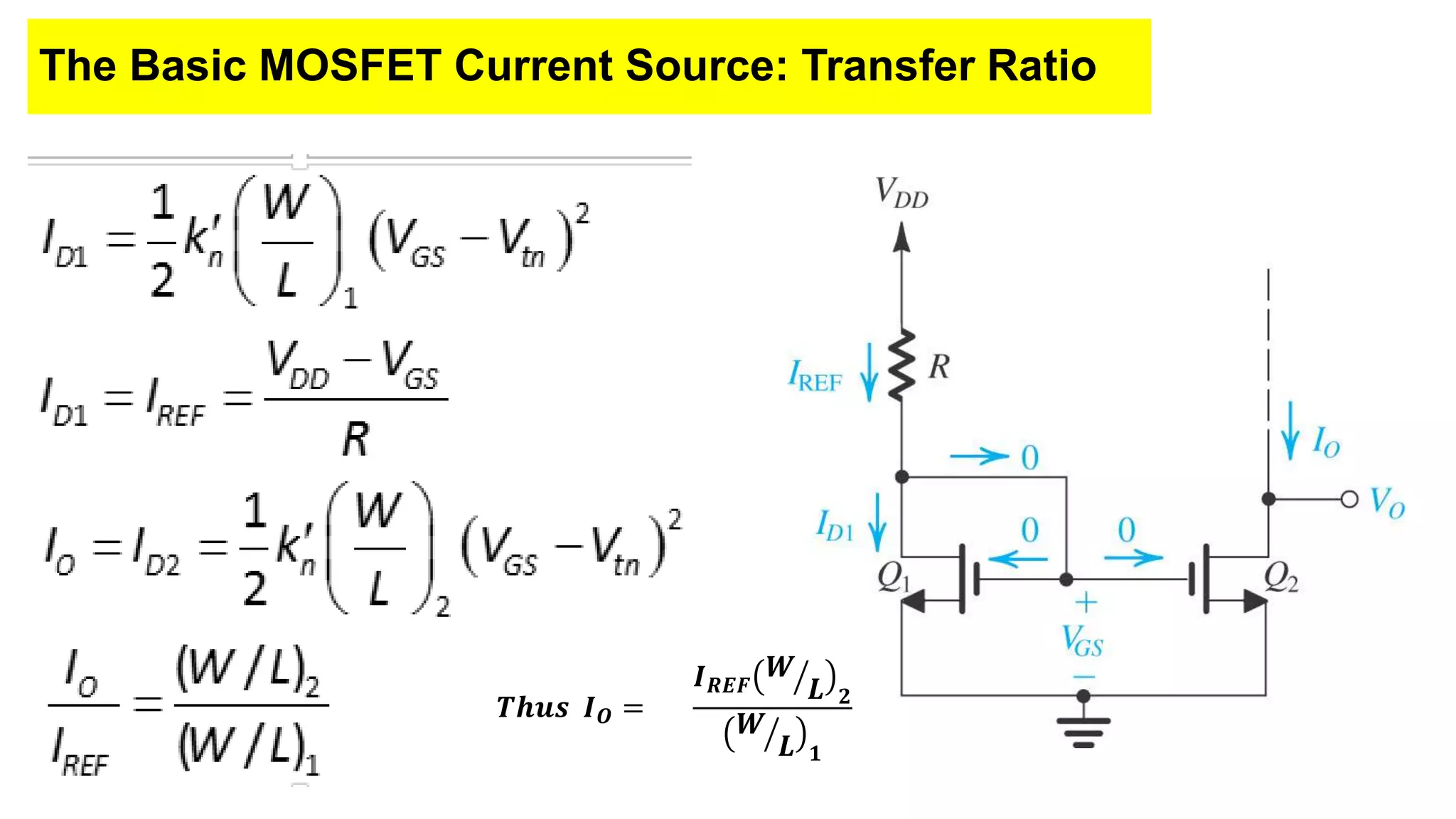
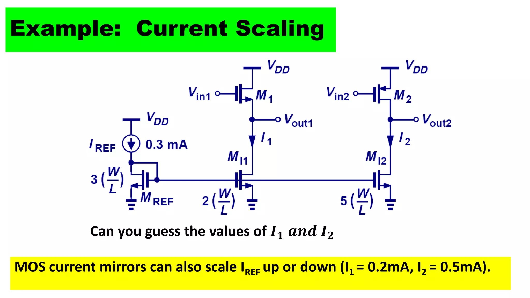
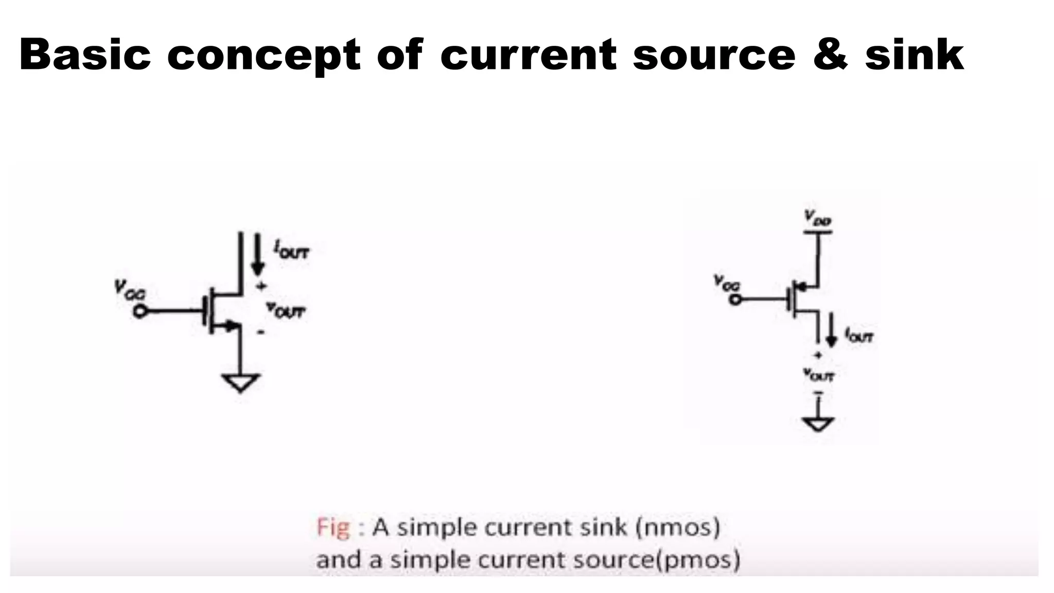
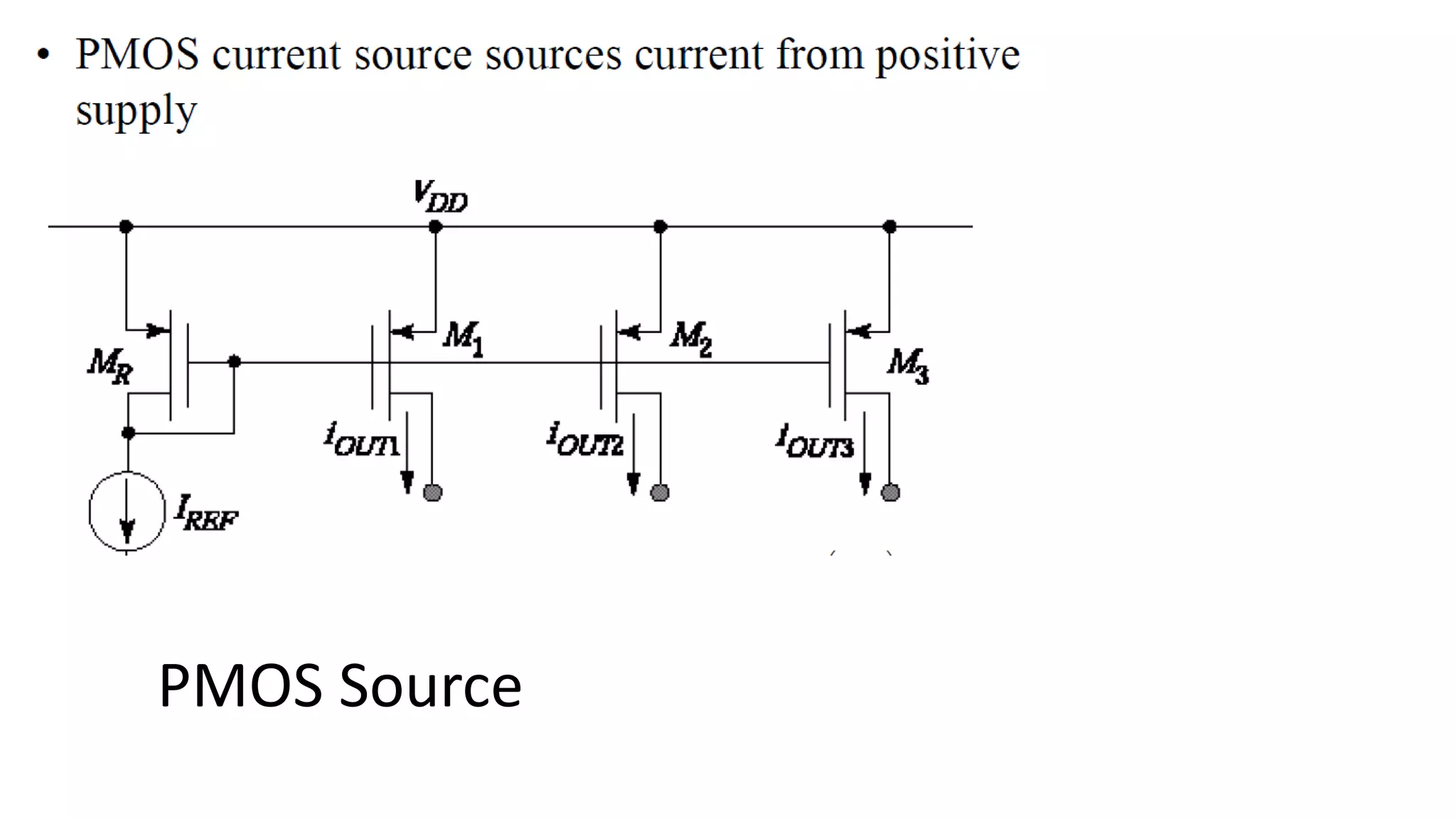
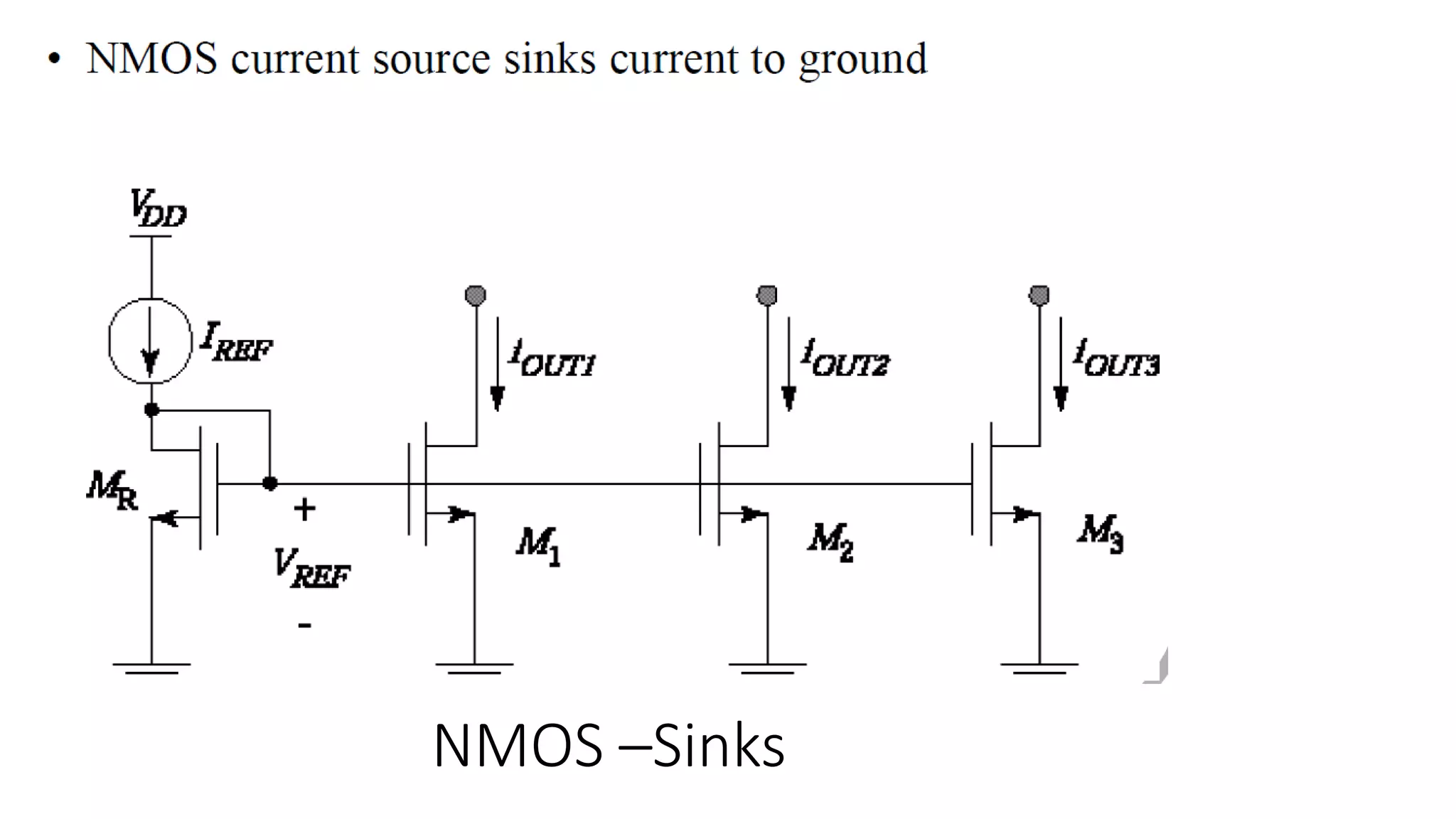
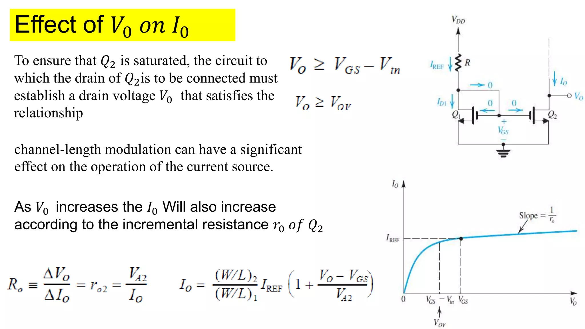
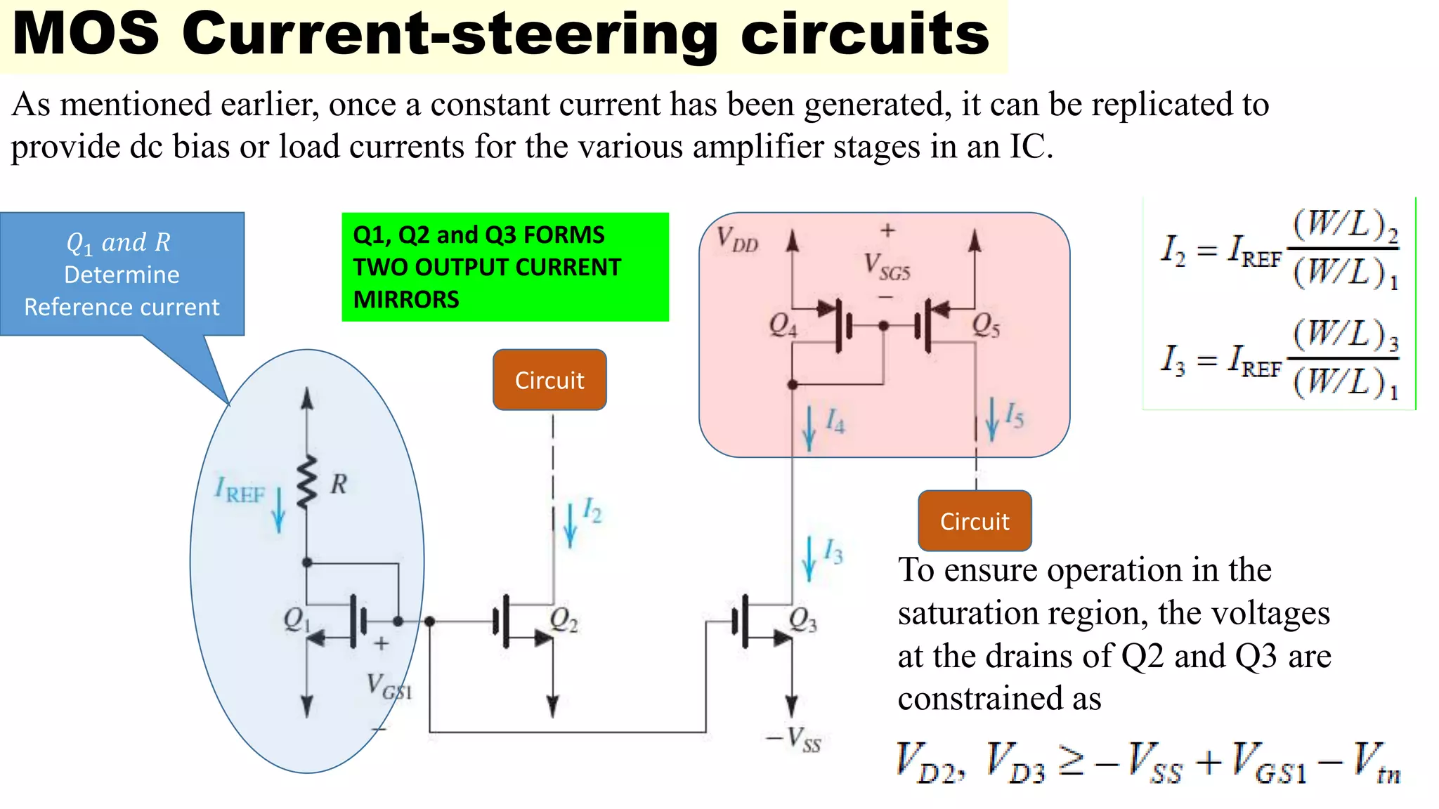
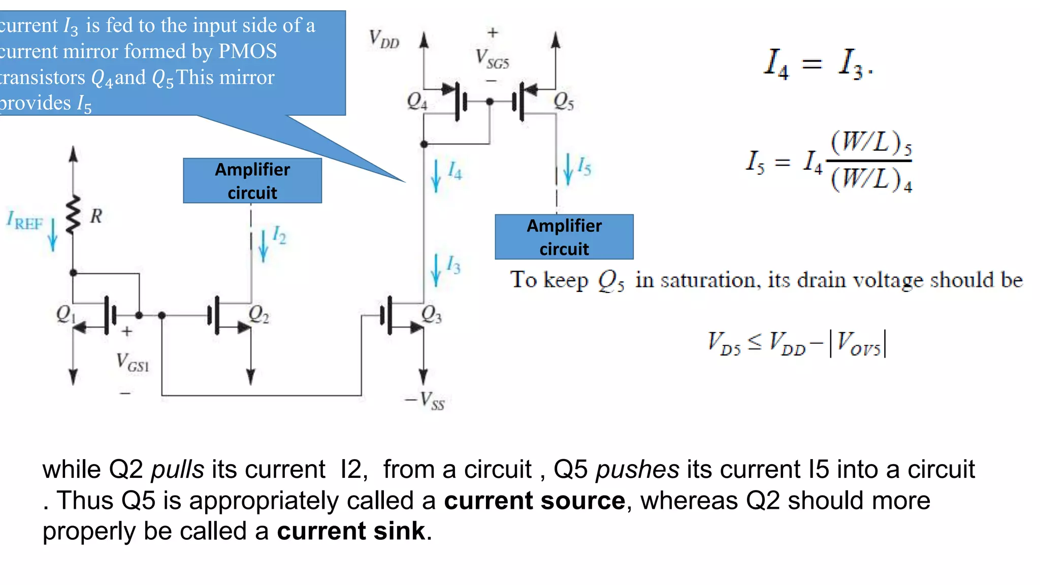
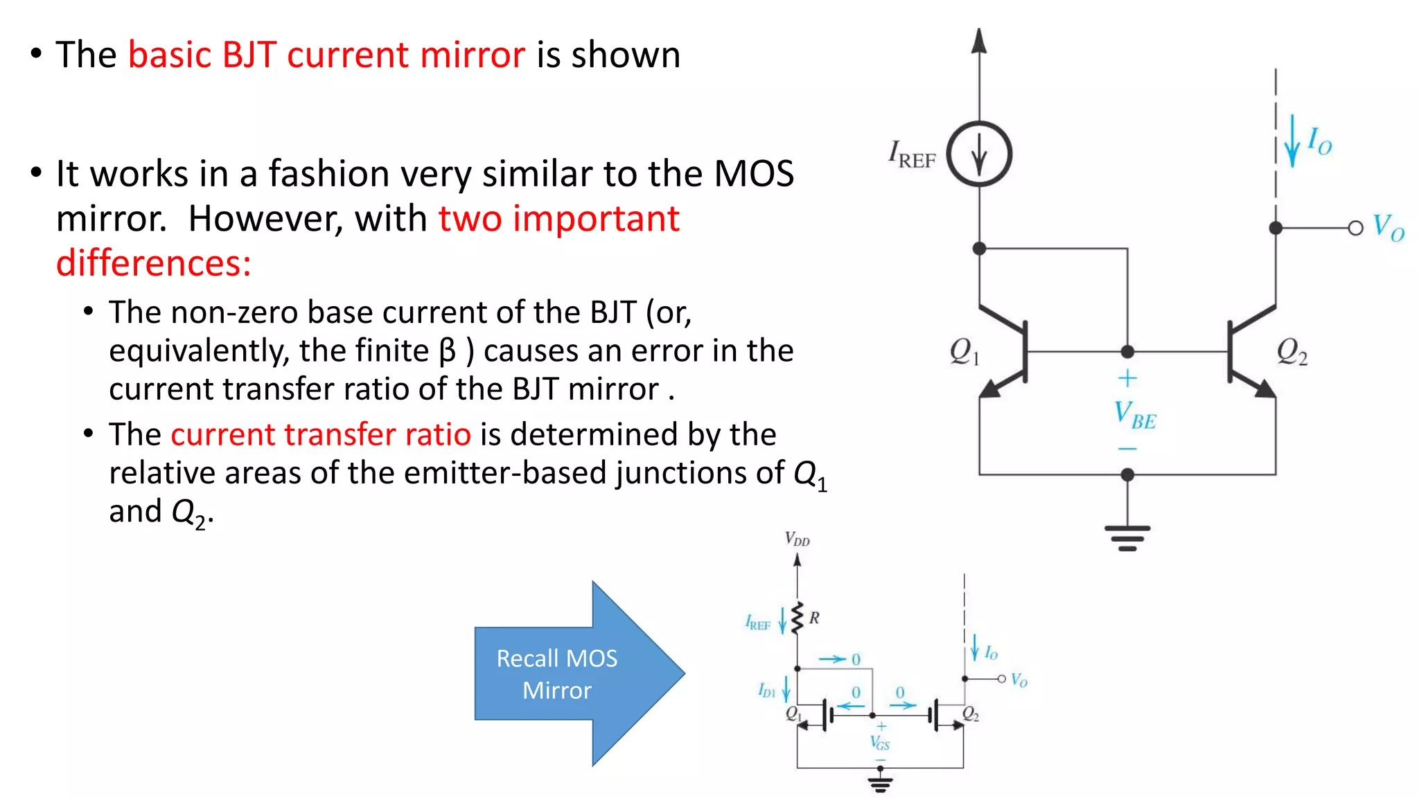
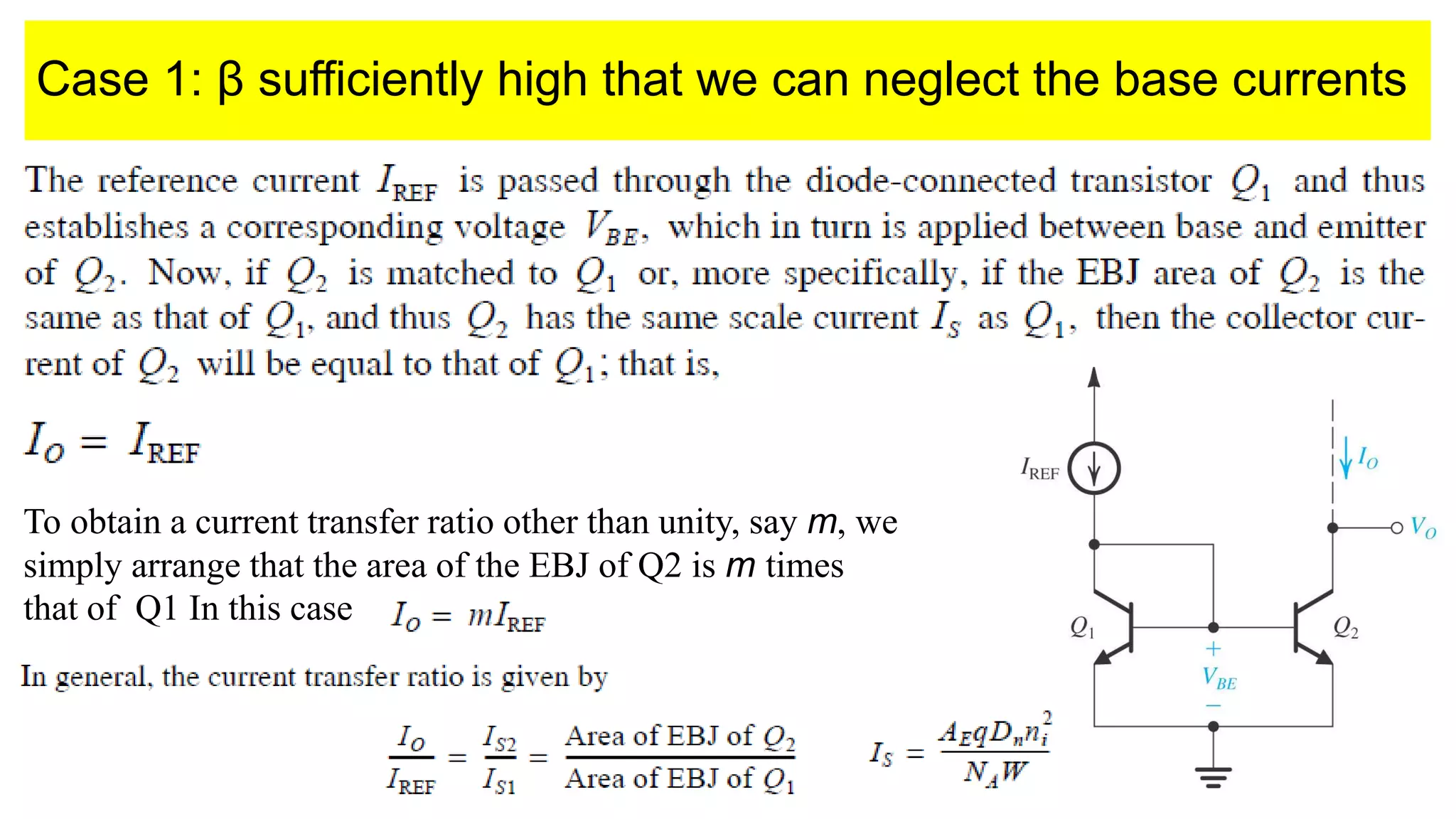
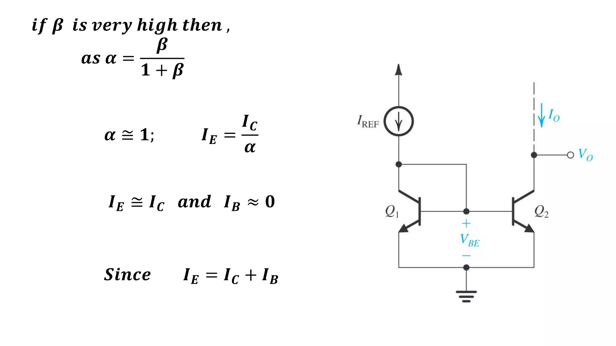
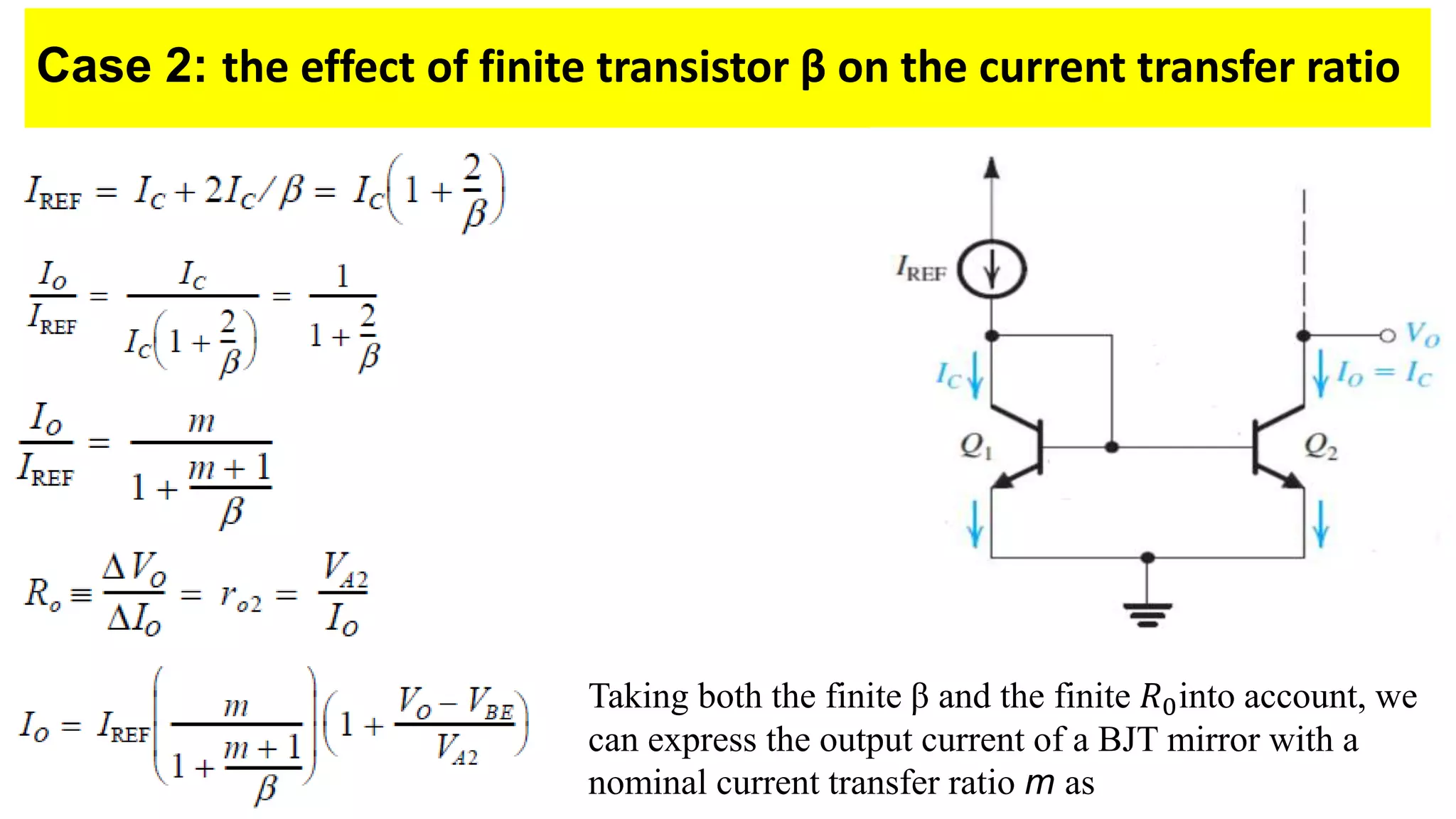
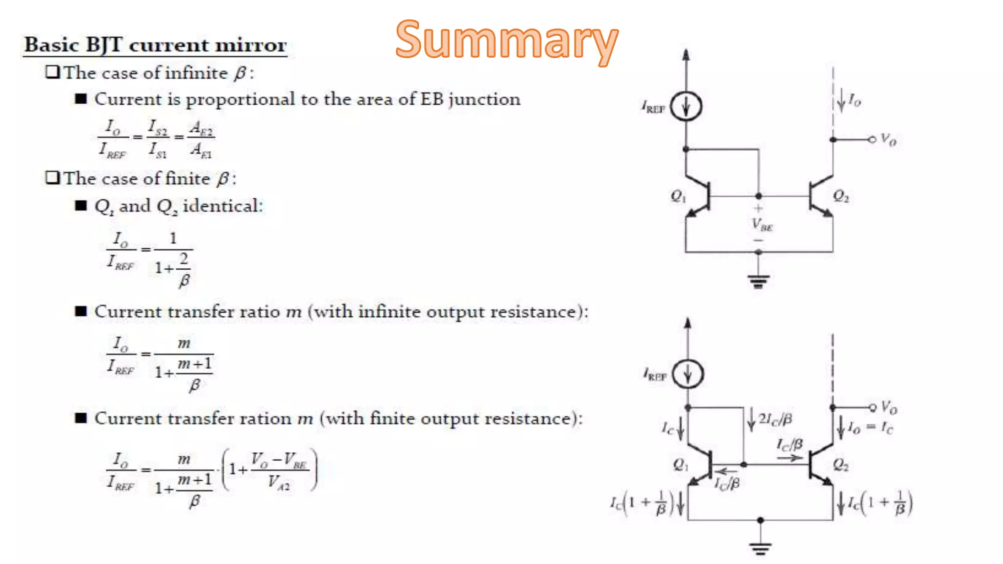
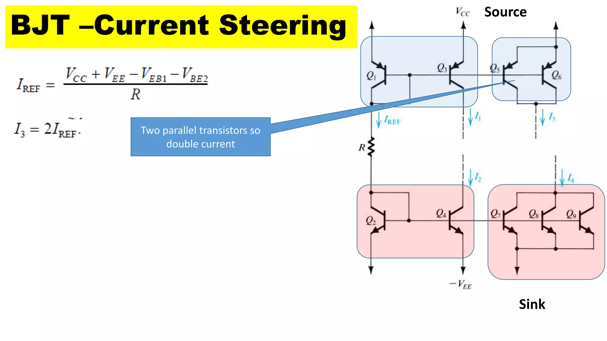
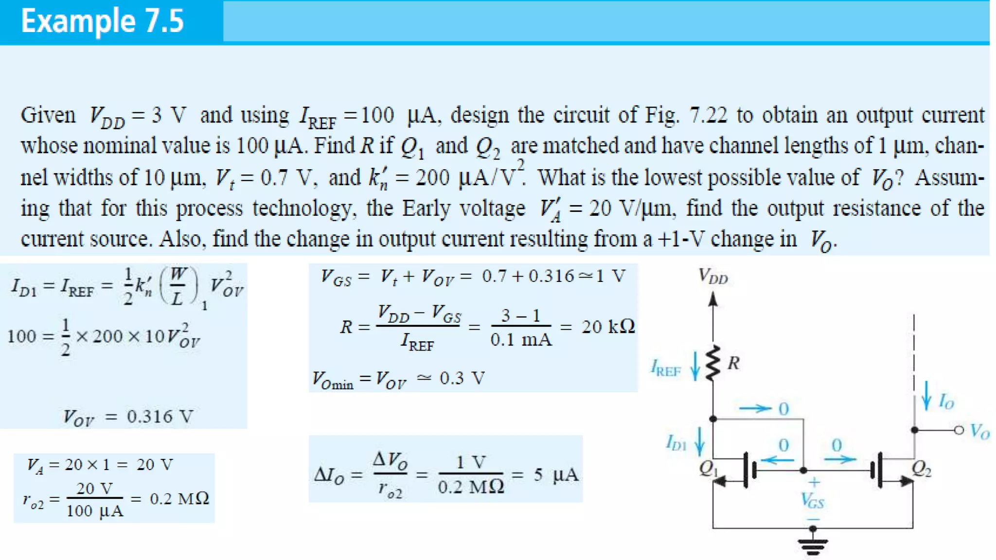
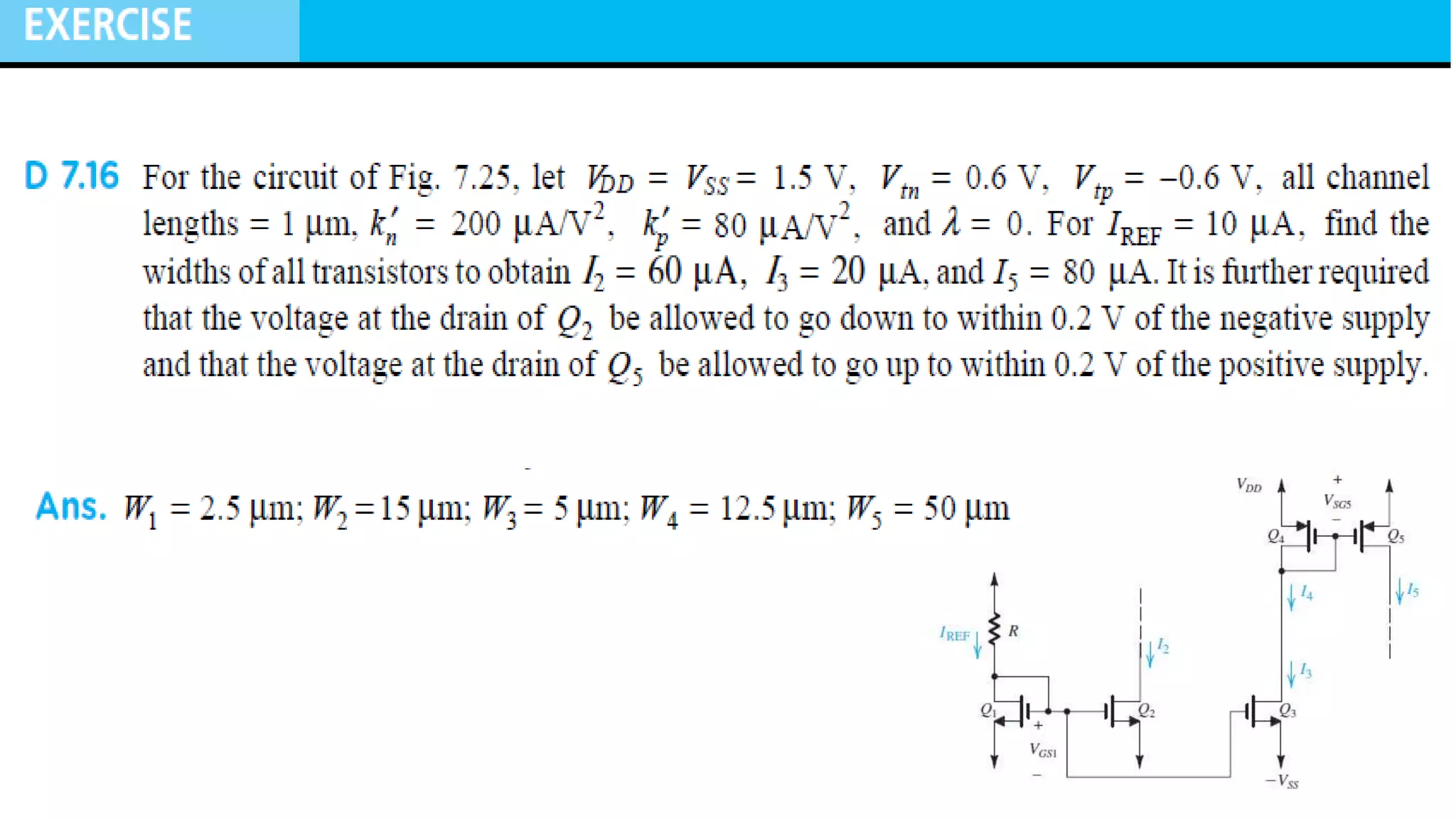
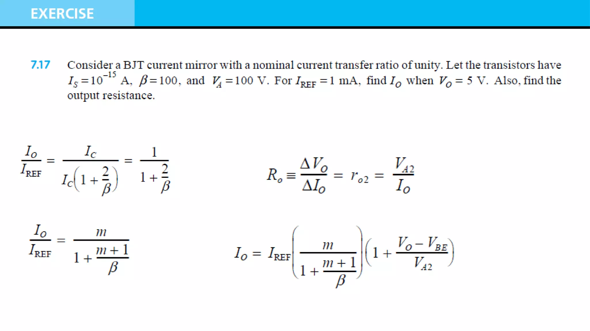
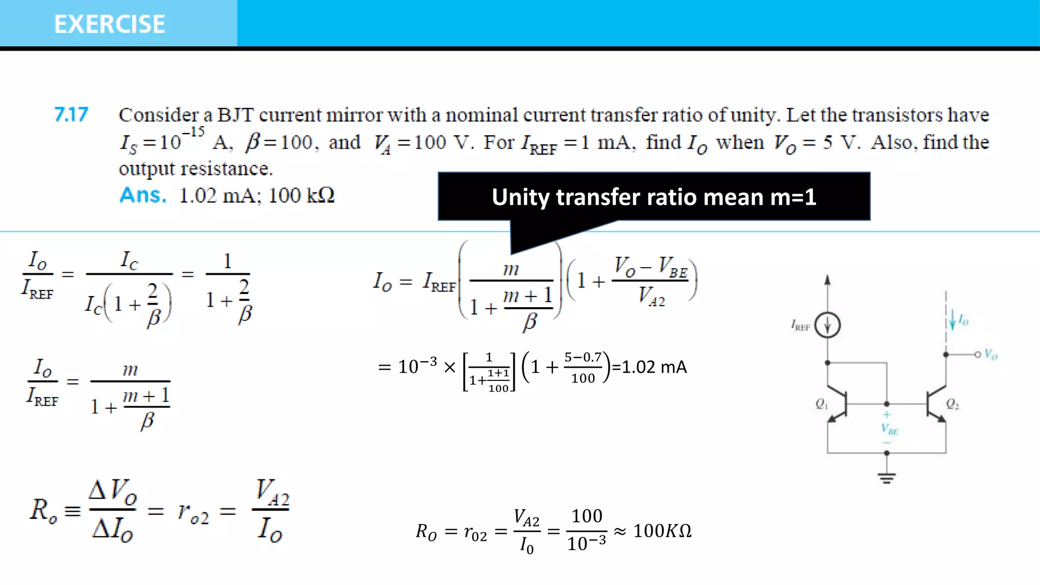
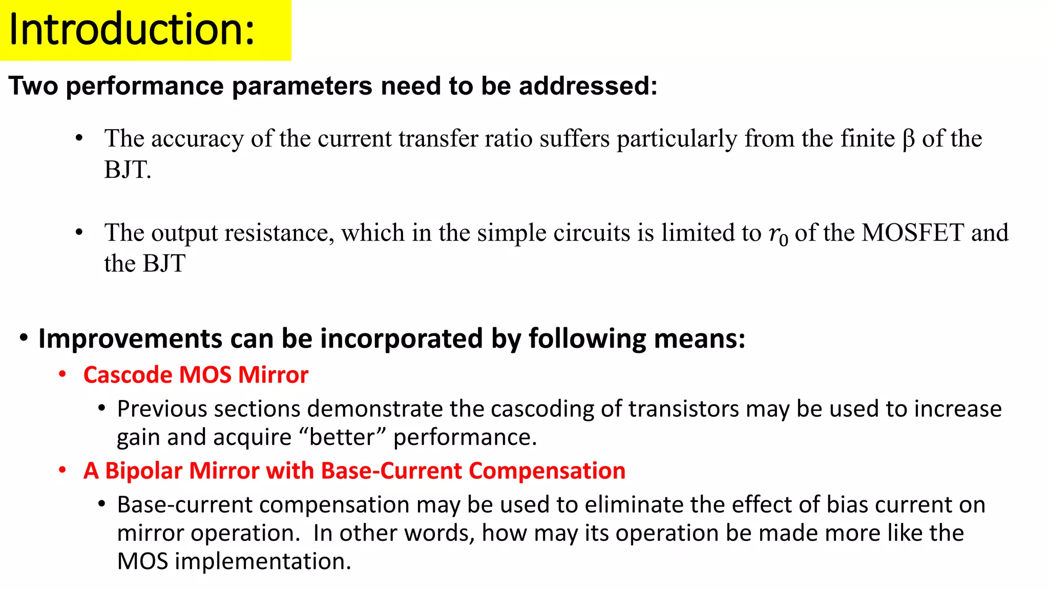
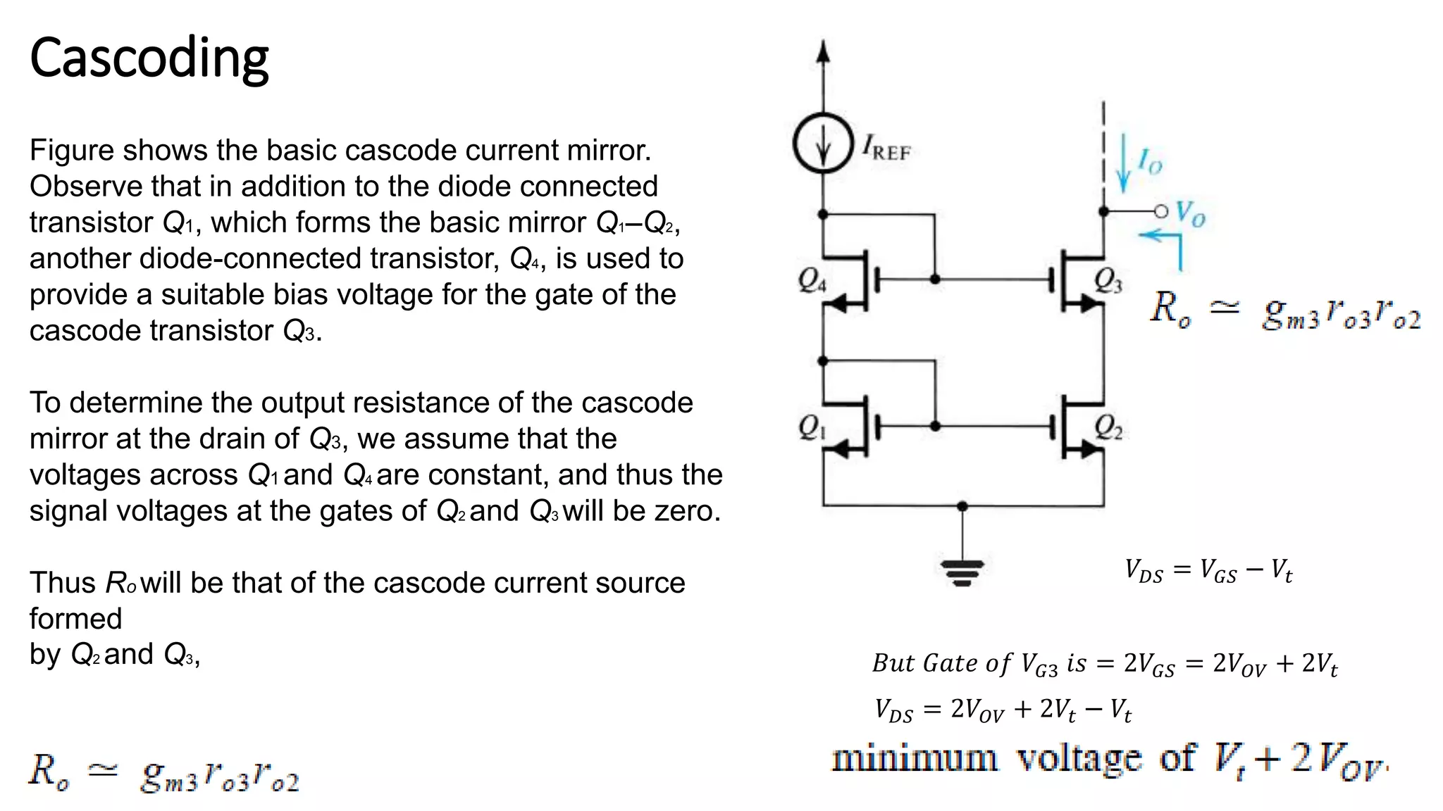
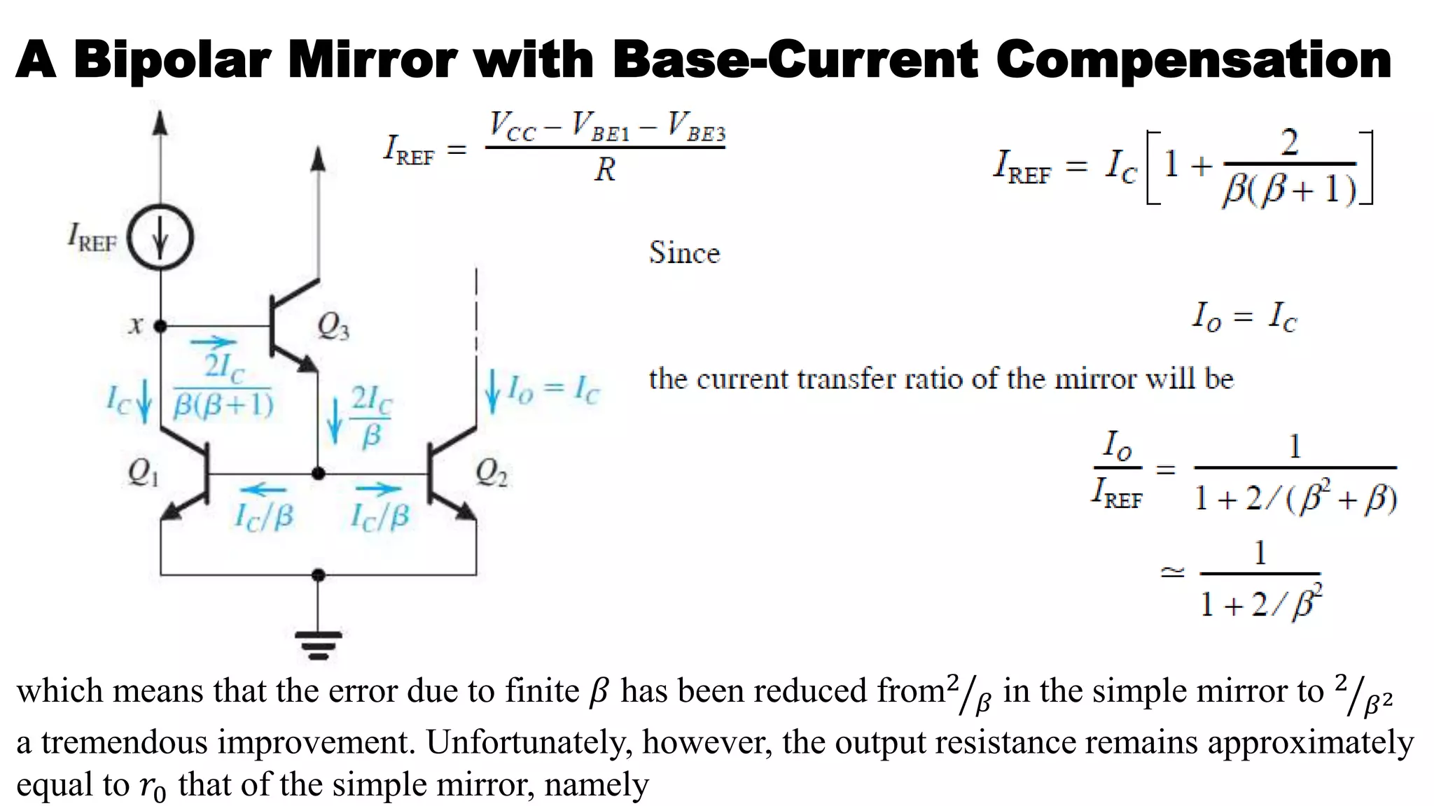
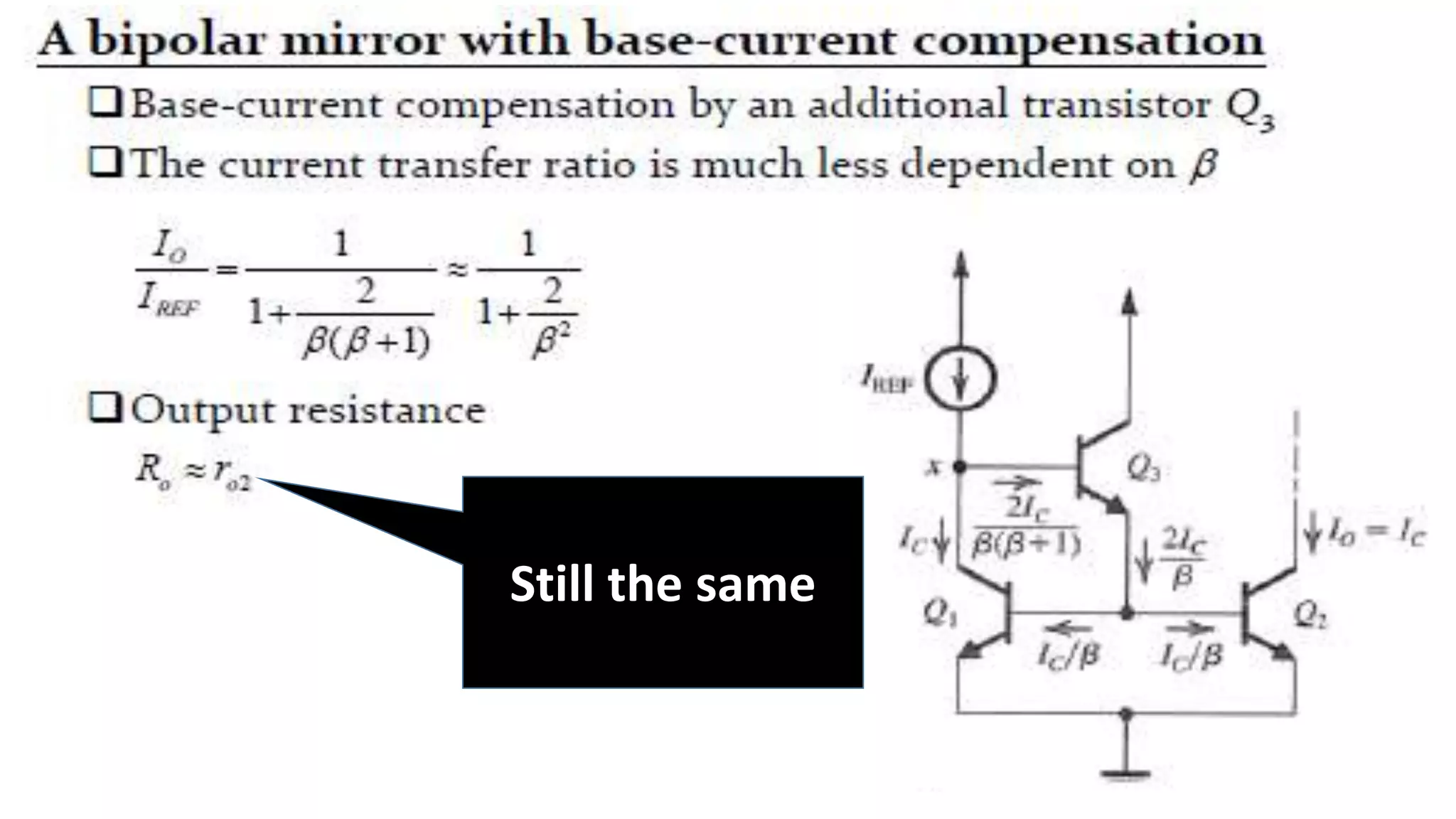
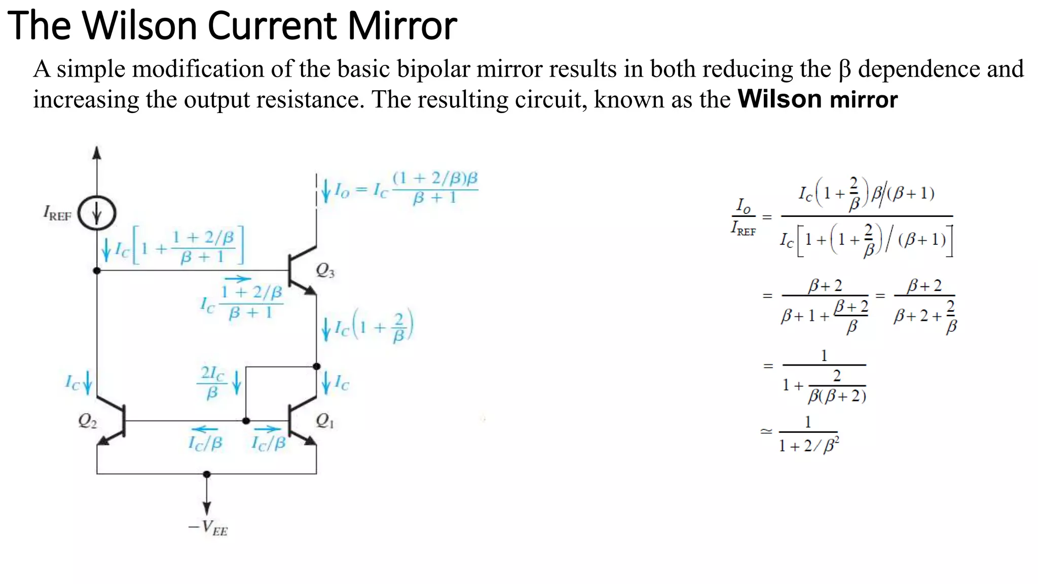
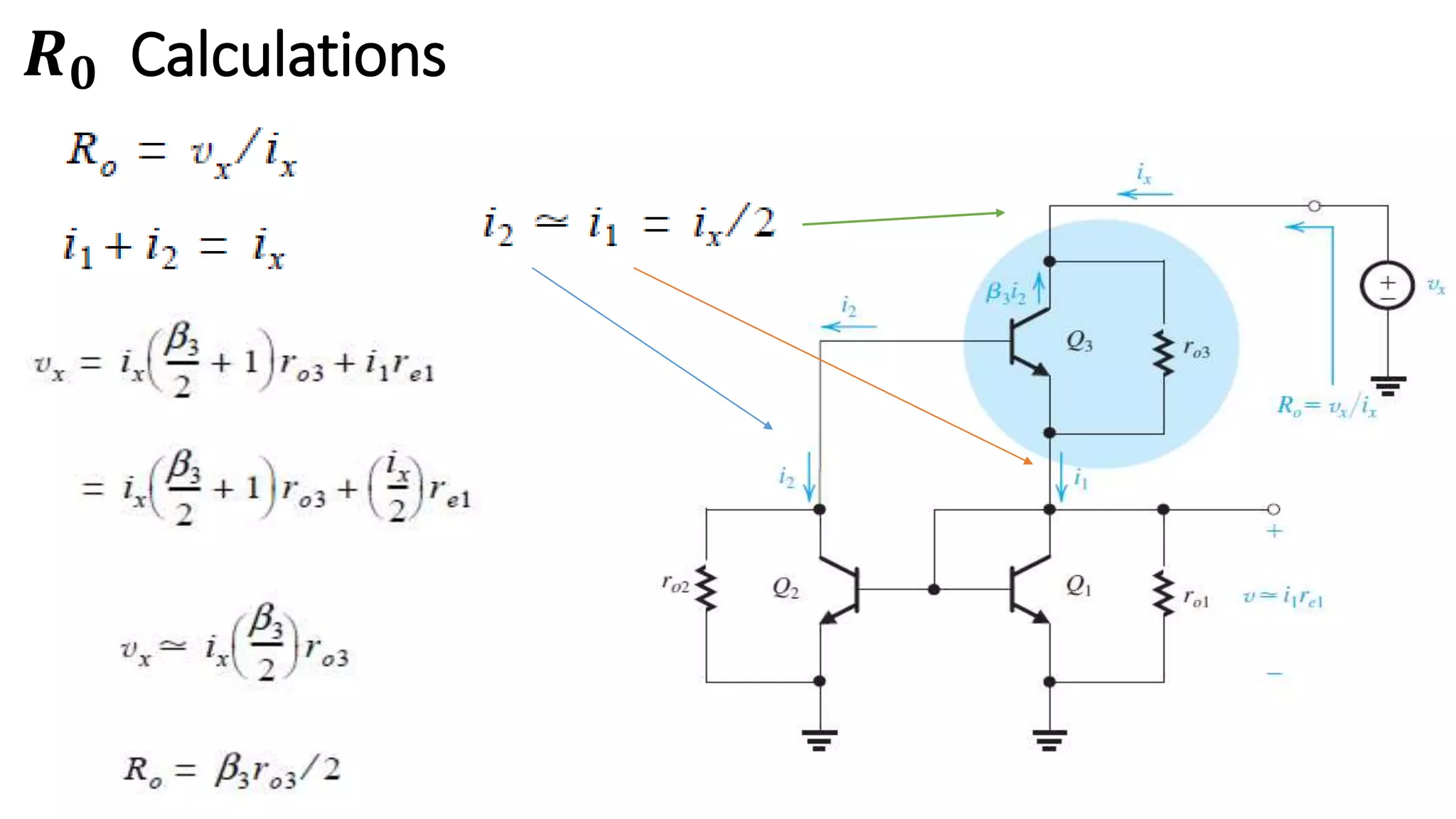
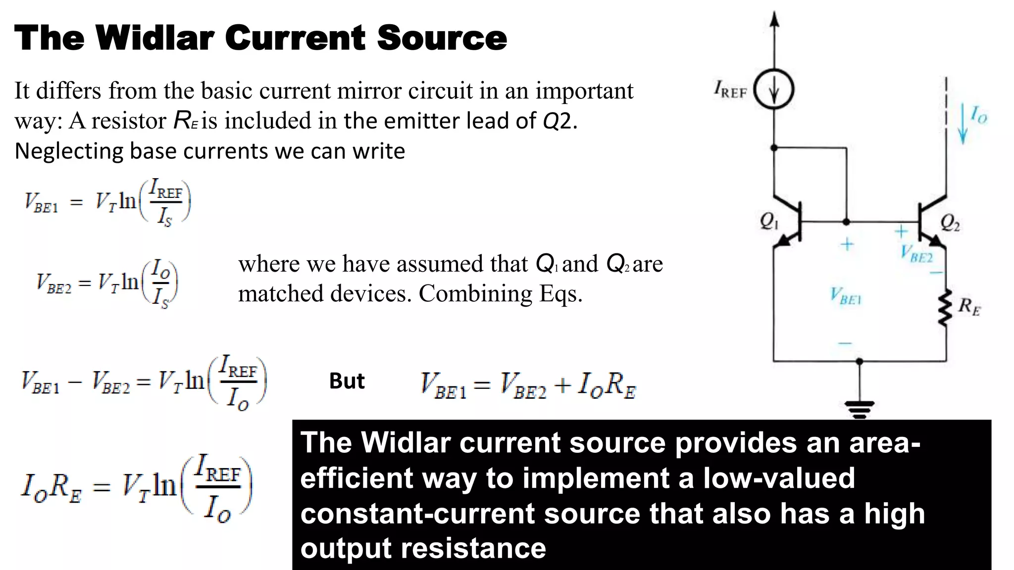
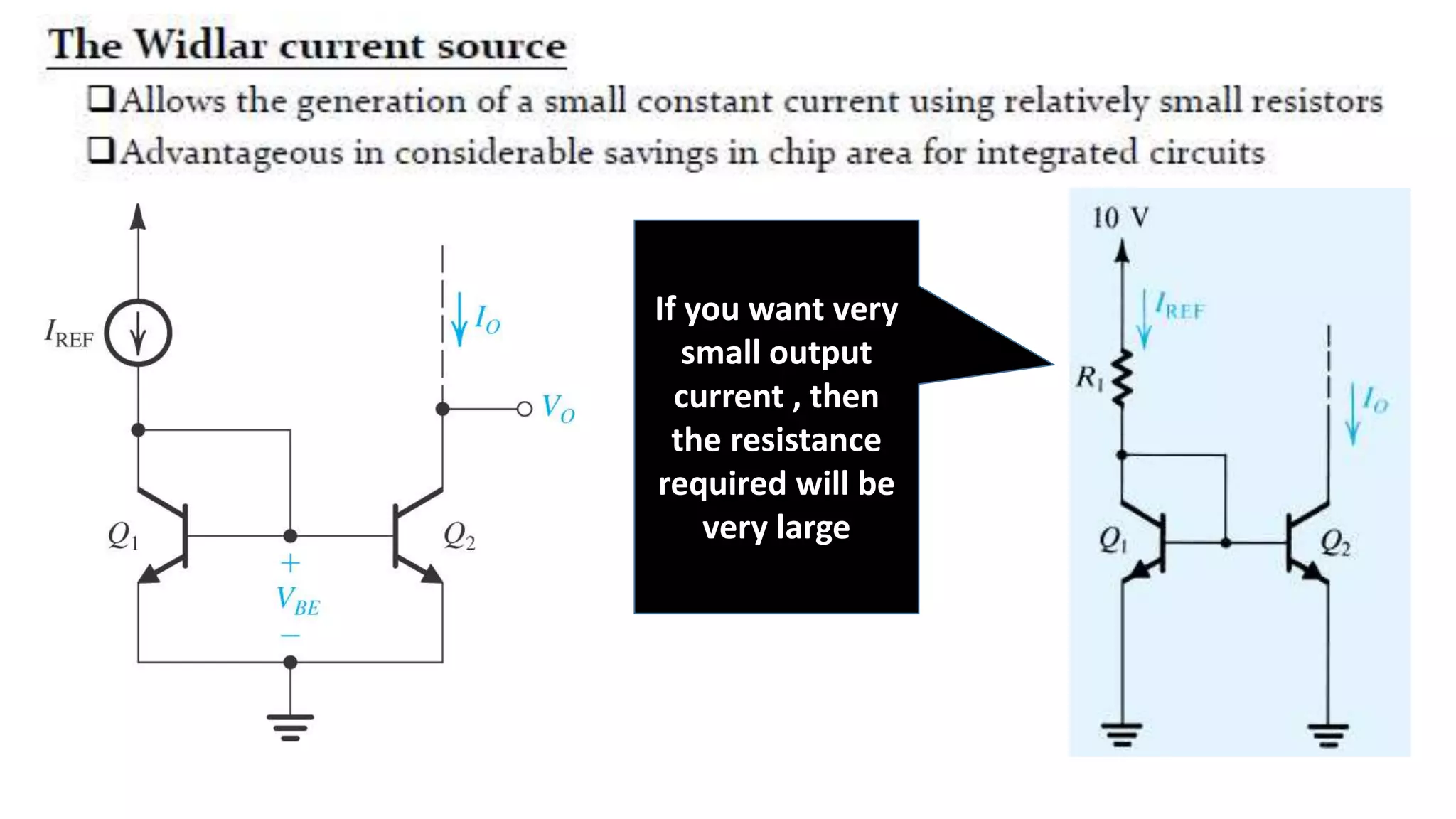
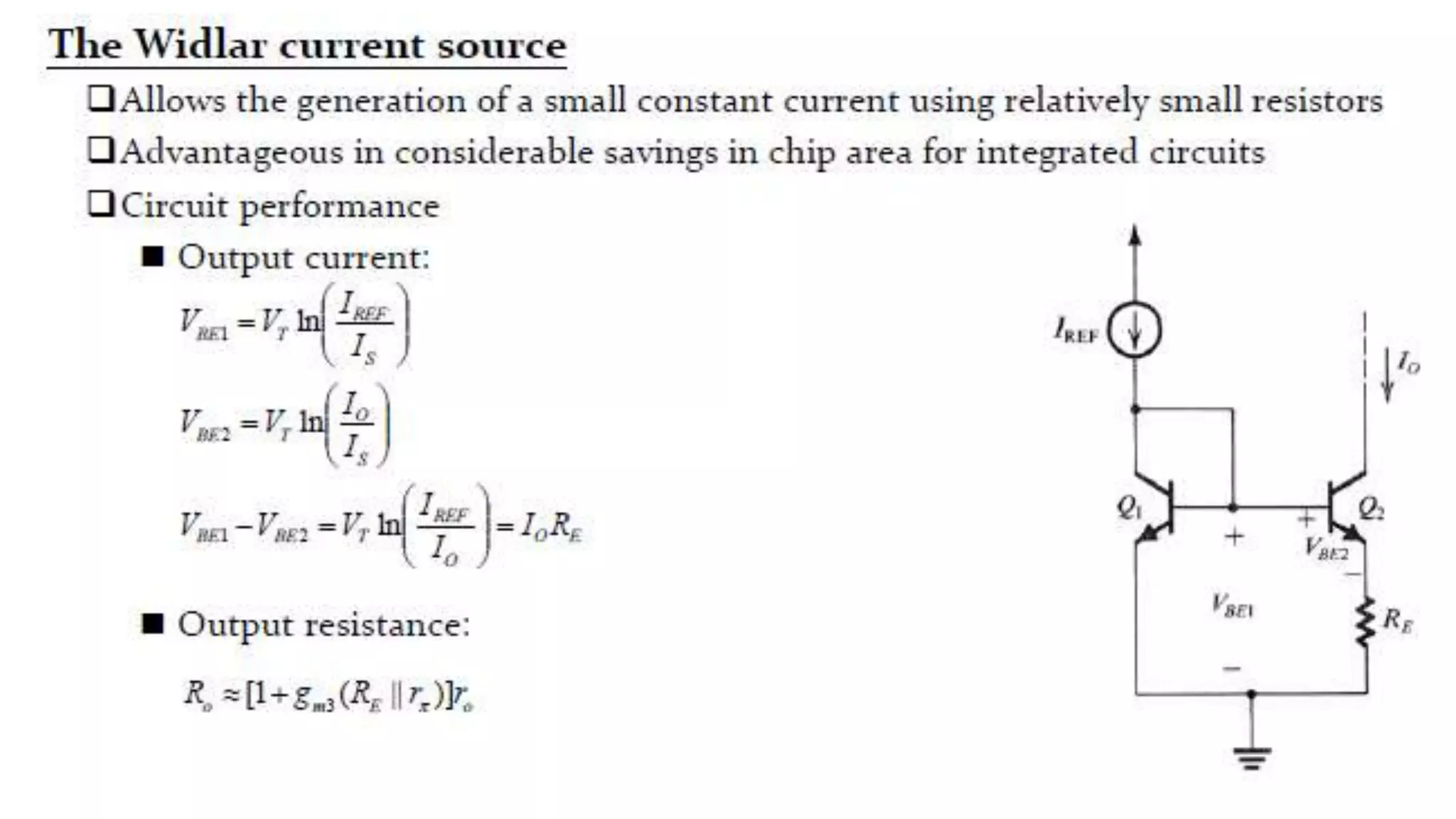
3. 7.4. IC Biasing – Current Sources, Current Mirrors, and
Current-Steering Circuits
• Biasing in integrated-circuit design is based on the use of constant-current
sources.
• On an IC chip with a number of amplifier stages, a constant dc current
(reference current) is generated at one location and is then replicated at
various other locations for biasing.
• This is known as current steering.
• This approach has the advantage that the effort expended on generating a
predictable and stable reference current need not be repeated.
4.
5. The current mirrors uses the principle that if
the gate –source potential of two identical
MOS transistors are equal then the current
flown through their Drain terminals should
be the same
NMOS current mirrors are used as
current sinks and PMOS current mirrors
are used as current sources
There is variety of current mirror circuits
available, each of them having their own
advantages and applications
BASIC PRINCIPLE
6. For proper operation,
the output terminal,
that is, the drain of
Q2, must be
connected to a circuit
that ensures that Q2
operates in
saturation.
7. The Basic MOSFET Current Source: Transfer Ratio
𝑻𝒉𝒖𝒔 𝑰𝑶 =
𝑰𝑹𝑬𝑭
𝑾
𝑳 𝟐
𝑾
𝑳 𝟏
8. 8
Example: Current Scaling
Can you guess the values of 𝑰𝟏 𝒂𝒏𝒅 𝑰𝟐
MOS current mirrors can also scale IREF up or down (I1 = 0.2mA, I2 = 0.5mA).
12. Effect of 𝑉0 𝑜𝑛 𝐼0
To ensure that 𝑄2 is saturated, the circuit to
which the drain of 𝑄2is to be connected must
establish a drain voltage 𝑉0 that satisfies the
relationship
channel-length modulation can have a significant
effect on the operation of the current source.
As 𝑉0 increases the 𝐼0 Will also increase
according to the incremental resistance 𝑟0 𝑜𝑓 𝑄2
13. MOS Current-steering circuits
As mentioned earlier, once a constant current has been generated, it can be replicated to
provide dc bias or load currents for the various amplifier stages in an IC.
𝑄1 𝑎𝑛𝑑 𝑅
Determine
Reference current
Q1, Q2 and Q3 FORMS
TWO OUTPUT CURRENT
MIRRORS
To ensure operation in the
saturation region, the voltages
at the drains of Q2 and Q3 are
constrained as
Circuit
Circuit
14. current 𝐼3 is fed to the input side of a
current mirror formed by PMOS
transistors 𝑄4and 𝑄5This mirror
provides 𝐼5
while Q2 pulls its current I2, from a circuit , Q5 pushes its current I5 into a circuit
. Thus Q5 is appropriately called a current source, whereas Q2 should more
properly be called a current sink.
Amplifier
circuit
Amplifier
circuit
16. • The basic BJT current mirror is shown
• It works in a fashion very similar to the MOS
mirror. However, with two important
differences:
• The non-zero base current of the BJT (or,
equivalently, the finite β ) causes an error in the
current transfer ratio of the BJT mirror .
• The current transfer ratio is determined by the
relative areas of the emitter-based junctions of Q1
and Q2.
Recall MOS
Mirror
17. Case 1: β sufficiently high that we can neglect the base currents
To obtain a current transfer ratio other than unity, say m, we
simply arrange that the area of the EBJ of Q2 is m times
that of Q1 In this case
19. Case 2: the effect of finite transistor β on the current transfer ratio
Taking both the finite β and the finite 𝑅0into account, we
can express the output current of a BJT mirror with a
nominal current transfer ratio m as
29. Introduction:
Two performance parameters need to be addressed:
• The accuracy of the current transfer ratio suffers particularly from the finite β of the
BJT.
• The output resistance, which in the simple circuits is limited to 𝑟0 of the MOSFET and
the BJT
• Improvements can be incorporated by following means:
• Cascode MOS Mirror
• Previous sections demonstrate the cascoding of transistors may be used to increase
gain and acquire “better” performance.
• A Bipolar Mirror with Base-Current Compensation
• Base-current compensation may be used to eliminate the effect of bias current on
mirror operation. In other words, how may its operation be made more like the
MOS implementation.
30. Cascoding
Figure shows the basic cascode current mirror.
Observe that in addition to the diode connected
transistor Q1, which forms the basic mirror Q1–Q2,
another diode-connected transistor, Q4, is used to
provide a suitable bias voltage for the gate of the
cascode transistor Q3.
To determine the output resistance of the cascode
mirror at the drain of Q3, we assume that the
voltages across Q1 and Q4 are constant, and thus the
signal voltages at the gates of Q2 and Q3 will be zero.
Thus Ro will be that of the cascode current source
formed
by Q2 and Q3,
𝑉𝐷𝑆 = 𝑉𝐺𝑆 − 𝑉𝑡
𝐵𝑢𝑡 𝐺𝑎𝑡𝑒 𝑜𝑓 𝑉𝐺3 𝑖𝑠 = 2𝑉𝐺𝑆 = 2𝑉𝑂𝑉 + 2𝑉𝑡
𝑉𝐷𝑆 = 2𝑉𝑂𝑉 + 2𝑉𝑡 − 𝑉𝑡
31. A Bipolar Mirror with Base-Current Compensation
which means that the error due to finite 𝛽 has been reduced from2
𝛽 in the simple mirror to 2
𝛽2
a tremendous improvement. Unfortunately, however, the output resistance remains approximately
equal to 𝑟0 that of the simple mirror, namely
33. The Wilson Current Mirror
A simple modification of the basic bipolar mirror results in both reducing the β dependence and
increasing the output resistance. The resulting circuit, known as the Wilson mirror
36. The Widlar Current Source
It differs from the basic current mirror circuit in an important
way: A resistor RE is included in the emitter lead of Q2.
Neglecting base currents we can write
where we have assumed that Q1 and Q2 are
matched devices. Combining Eqs.
But
The Widlar current source provides an area-
efficient way to implement a low-valued
constant-current source that also has a high
output resistance
37. If you want very
small output
current , then
the resistance
required will be
very large
38.
39. Some Useful Transistor Pairings
• The cascode configuration studied in Section 7.3 combines CS and
CG MOS transistors (CE and CB bipolar transistors) to great
advantage.
• The key to the superior performance of the resulting combination is
that the transistor pairing is done in a way that maximizes the
advantages and minimizes the shortcomings of each of the two
individual configurations.
• In this section we present a number of other such transistor pairings.
In each case the transistor pair can be thought of as a compound
device; thus the resulting amplifier may be considered as a single
stage.
40. 1. The CC–CE, CD–CS, and CD–CE
Configurations
2. The CC–CB and CD–CG Configurations
Some Useful Transistor Pairings
41. 1. The CC–CE Configurations
Figure shows an amplifier formed by cascading a
common-collector (emitter follower) transistor 𝑸𝟏 with
a common-emitter transistor 𝑸𝟐
This circuit has two main advantages over the CE
amplifier.
• First, the emitter follower increases the input
resistance by a factor equal to 𝟏 + 𝜷𝟏 As a result,
the overall voltage gain is increased, especially if the
resistance of the signal source is large.
• Second, the CC–CE amplifier can exhibit much wider
bandwidth than that obtained with the CE
amplifier.
42. 1. The CD–CS Configurations
The MOS counterpart of the CC–CE
amplifier, namely, the CD–CS
configuration, is shown.
Here, the CS amplifier alone has an
infinite input resistance,
• The sole purpose for adding the
source-follower stage is to
increase the amplifier
bandwidth,
43. 1. The CC–CE Configurations
Fig. shows the BiCMOS version of
this circuit type.
• Compared to the bipolar circuit ,
the BiCMOS circuit has an
infinite input resistance.
• Compared to the MOS circuit ,
the BiCMOS circuit typically has
a higher 𝒈𝒎𝟐
44. The Darlington Configuration
It can be thought of as a variation of the CC–CE circuit with the collector
of 𝑄1connected to that of 𝑄2
Alternatively, the Darlington pair can be thought of as a composite
transistor with 𝛽 = 𝛽1 × 𝛽2 It can therefore be used to implement a high-
performance voltage follower
Since the transistor β depends on the dc bias
current, it is possible that 𝑄1will be operating at
a very low β, rendering the β-multiplication
effect of the Darlington pair rather ineffective. A
simple solution to this problem is to provide a
bias current for 𝑄1
Note that in this application the circuit
can be considered as the cascade
connection of two common-collector
transistors (i.e., a CC–CC
configuration).
1. The CC–CE Configurations (Variation )
46. Cascading an emitter follower with a common-
base amplifier, results in a circuit with a low-
frequency gain approximately equal to that of
the CB but with
the problem of the low input resistance of the CB
solved by the buffering action of the CC stage.
It will be shown in Chapter 9 that this circuit
exhibits wider bandwidth than that obtained
with a CE amplifier of the same gain
Note that the biasing current sources ensure that each of 𝑸𝟏and 𝑸𝟐is operating at a bias
current I. We are not showing, however, how the dc voltage at the base of 𝑸𝟏is set or the
circuit that determines the dc voltage at the collector of 𝑸𝟐: Both issues are usually
looked after in the larger circuit of which the CC–CB amplifier is a part.
47. The MOSFET version of the
circuit is the CD–CG amplifier
An interesting version of the CC–CB
configuration is shown in Fig.on left
Here the CB stage is implemented with a pnp
transistor.
Although only one current source is now
needed, observe that we also need to establish
an appropriate bias voltage at the base of 𝑄2
48. Assignment No 2 (CLO-1)
(Submission date 10th October 2022)
•Do all examples and exercise starting from page
542 to page 552) of your text book
“Microelectronics Circuits” 6th edition by Sedra &
Smith
•You are also given an assignment( Assignment 3)
to be submitted on 5th Oct. The asc. Files have
been emailed to all three section.
49.
50. We observe that using the Widlar circuit allows the
generation of a small constant current using relatively
small resistors
𝑉𝐵𝐸 for both the transistors not same
Now 𝑉𝐸 = 0.115 ; and 𝑉𝐵𝐸2 = 0.585
0.115 V less then Q1
54. The Darlington Configuration
(a) The Darlington configuration; (b) voltage follower using the Darlington configuration; (c) the
Darlington follower with a bias current I supplied to Q1 to ensure that its β remains high.
In one package