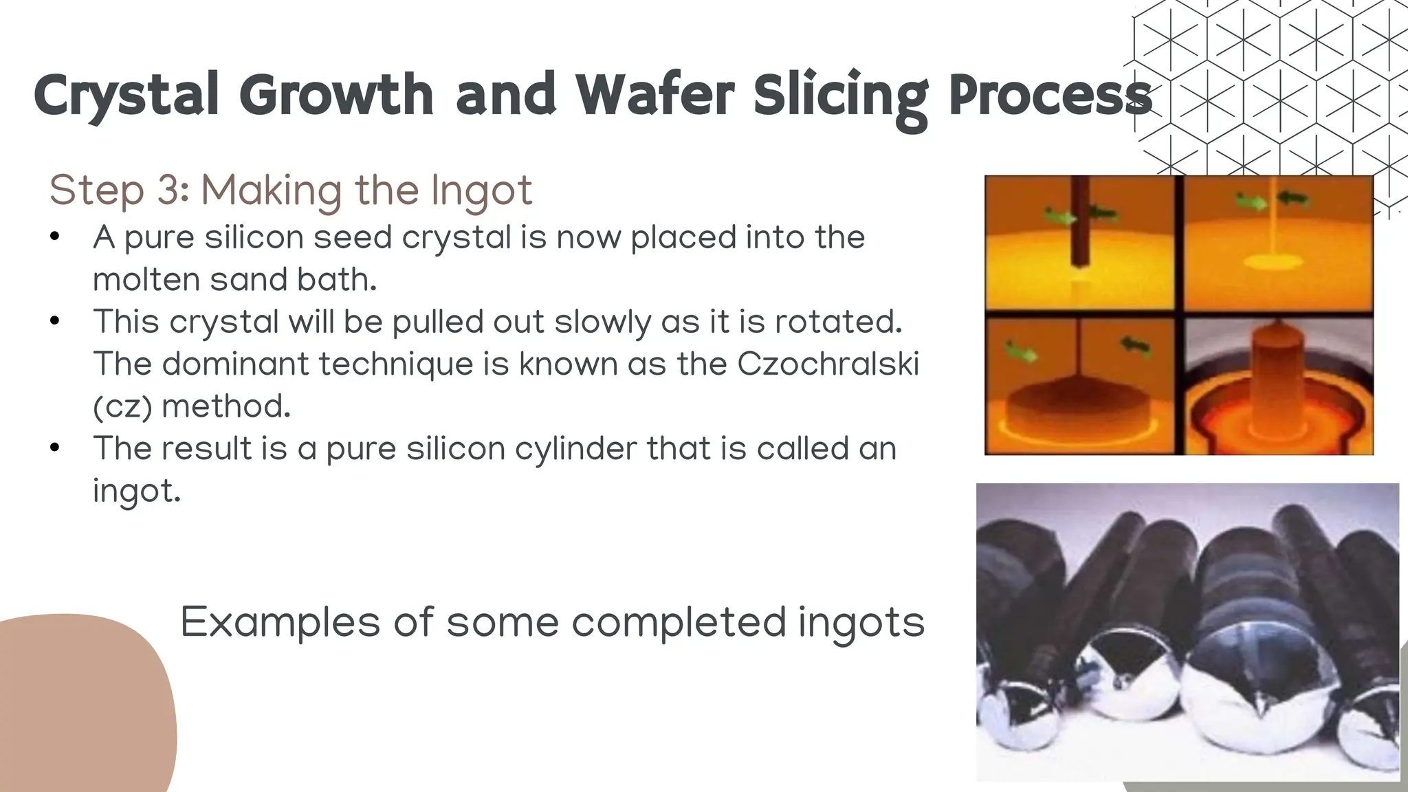
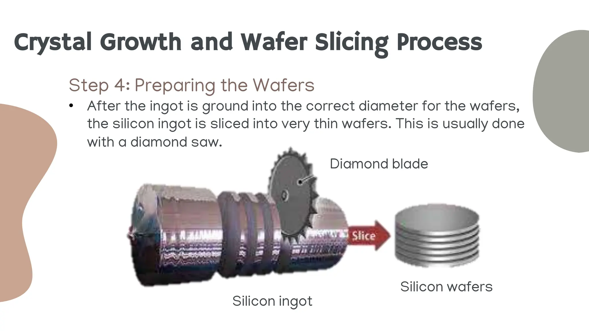
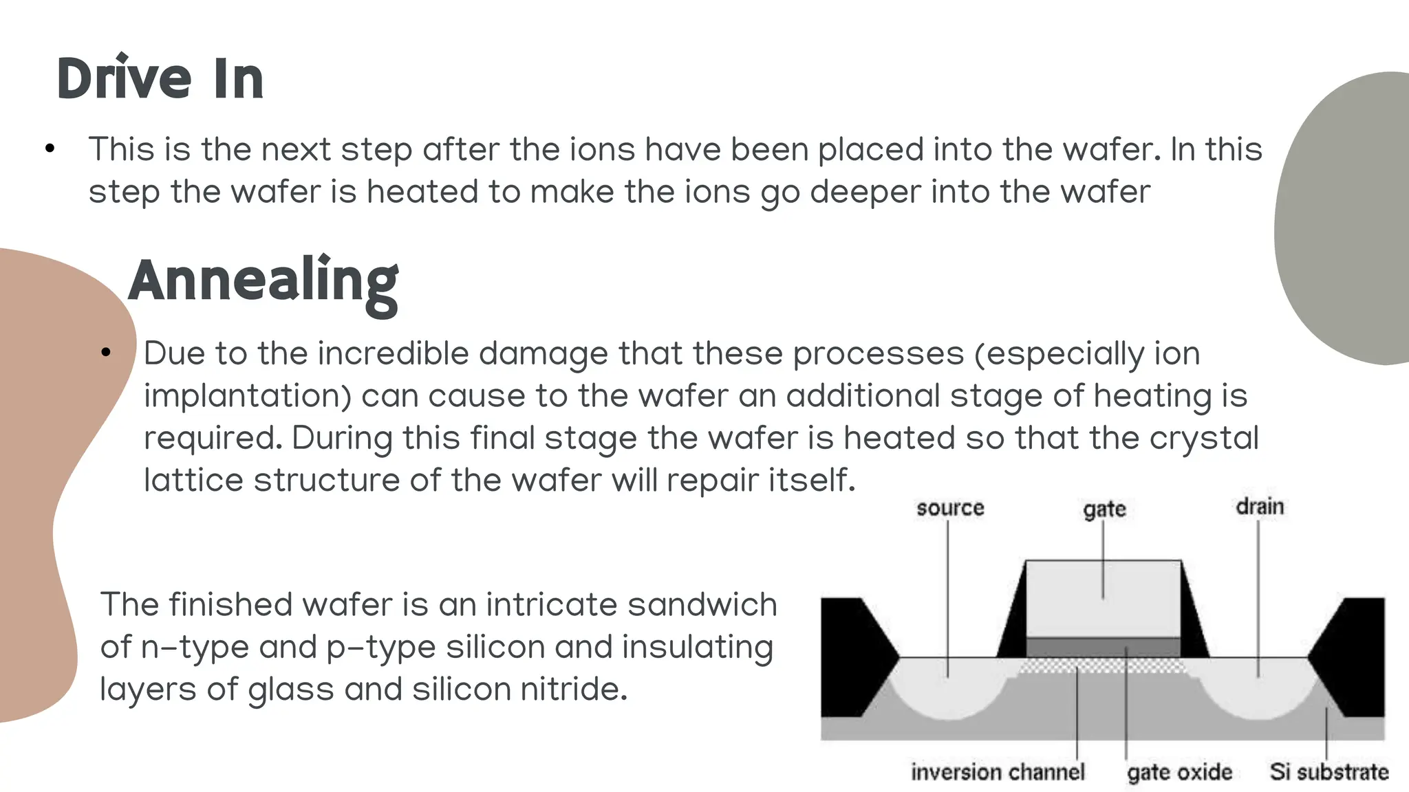
Preparation & Processing
of a Silicon Wafer
The processes needed to create & convert a blank wafer to
a patterned one
Turning silicon into
memory chips
Table of contents
Preparation of the
Silicon Wafer
Silicon Wafer
Processing Steps
Eliminate unsatisfactory
wafer materials from the
process stream
01 02
Preparation of
the Silicon Wafer
01
Crystal Growth and Wafer Slicing Process
Step 1: Obtaining the Sand
• The sand used to grow the wafers has to be a very clean and good form of
silicon
Step 2: Preparing the Molten Silicon Bath
• The sand (SiO2)is taken and put into a crucible and is heated to about 1600
degrees C – just above its melting point.
• The molten sand will become the source of the silicon that will be the wafer.
Crystal Growth and Wafer Slicing Process
Step 3: Making the Ingot
• A pure silicon seed crystal is now placed into the
molten sand bath.
• This crystal will be pulled out slowly as it is rotated.
The dominant technique is known as the Czochralski
(cz) method.
• The result is a pure silicon cylinder that is called an
ingot.
Examples of some completed ingots
Crystal Growth and Wafer Slicing Process
Step 4: Preparing the Wafers
• After the ingot is ground into the correct diameter for the wafers,
the silicon ingot is sliced into very thin wafers. This is usually done
with a diamond saw.
Diamond blade
Silicon wafers
Silicon ingot
Thickness Sorting
• Following slicing, silicon wafers are often sorted on an automated
basis into batches of uniform thickness to increase productivity in
the next process step.
Lapping & Etching Processes
• Lapping removes the surface silicon which has been
cracked or otherwise damaged by the slicing process, and
assures a flat surface.
• Wafers are then etched in a chemically active reagent to
remove any crystal damage remaining from the previous
process step.
Polishing Process
• Polishing is a chemical/mechanical process that smoothes the uneven
surface left by the lapping and etching processes and makes the wafer flat
and smooth enough to support optical photolithography.
A wafer polishing machine
Silicon Wafer
Processing Steps
02
Fabrication
• Semiconductor memory chips are manufactured in cleanroom environments
because the circuitry is so small even tiny bits of dust can damage it.
Class 1 Cleanroom
• There is no more than 1 particle of dust in a cubic foot of air.
• In comparison, a clean, modern hospital has about 10,000 dust particles per
cubic foot.
• The air inside a cleanroom is filtered and recirculated continuously, and
employees wear special clothing such as dust-free gowns, caps, and masks to
help keep the air particle-free.
Class 10 Cleanroom
• When wafers move into the process part of the machine, they are
contained in a vacuum, with extremely low particle contamination
levels.
Glass(silicon dioxide)layer
• At the beginning of the production process, the bare silicon
wafer is covered with a thin glass layer followed by a nitride
layer.
• The glass layer is formed by exposing the silicon wafer to
oxygen at temperatures of 900 degrees C or higher for an hour
or more, depending on how thick a layer is required.
• Glass (silicon dioxide) is formed in the silicon material by
exposing it to oxygen.
• At high temperatures, this chemical reaction (called oxidation)
occurs at a much faster rate.
Photolithography
• The wafer is uniformly coated with a thick light-sensitive liquid called photoresist.
• Portions of the wafer are selected for exposure by carefully aligning a mask
between an ultraviolet light source and the wafer. In the transparent areas of the
mask, light passes through and exposes the photoresist.
• Photoresist hardens and becomes impervious to etchants when exposed to
ultraviolet light. This chemical change allows the subsequent developer solution to
remove the unexposed photoresist while leaving the hardened, exposed
photoresist on the wafer.
Etching the Wafer Surface
• The etching process is used immediately after photolithography to
etch the unwanted material from the wafer.
• This process is not selective and that is why the pattern had to be
traced onto the wafer using photoresist.
Wet Etching
• Wet etching is done with the use of chemicals.
• A batch of wafers is dipped into a highly concentrated pool of
acid and the exposed areas of the wafer are etched away.
• Wet etching does not allow the smaller critical geometries
that are needed for todays chips.
Acid being poured
onto a wafer
Dry Etching
• Dry etching refers to any of the methods of etching that use
gas instead of chemical etchants.
• Dry etching is capable of producing critical geometries
that are very small.
Diffusion
• Diffusion is done in a furnace with a flow of gas running over the wafers.
• It is a way of introducing impurities or dopants into a silicon wafer to
change its electrical properties
• This step, like etch, is not selective so the photoresist and patterning need
to be done before this step.
• A diffusion chamber is capable of handling many wafers.
Ion Implantation
• ion implantation shoots the desired dopant ions into the wafer.
• Ion implantation has been best equated with firing a machine
gun into a wall. In this analogy the wall is the wafer and the
bullets are the ions.
• The main disadvantage of ion implantation is that it can only
process a single wafer at a time
The magnets used to
control the ion beam
Drive In
• This is the next step after the ions have been placed into the wafer. In this
step the wafer is heated to make the ions go deeper into the wafer
Annealing
The finished wafer is an intricate sandwich
of n-type and p-type silicon and insulating
layers of glass and silicon nitride.
• Due to the incredible damage that these processes (especially ion
implantation) can cause to the wafer an additional stage of heating is
required. During this final stage the wafer is heated so that the crystal
lattice structure of the wafer will repair itself.
Die Attach / Wire Bond
• Before the die are encapsulated, they are mounted on to lead frames,
and thin gold wires connect the bonding pads on the chip to the frames
to create the electrical path between the die and lead fingers.
Encapsulation
• During Encapsulation, lead frames are placed onto mold plates and heated.
• Molten plastic material is pressed around each die to form its individual package.
• The mold is opened, and the lead frames are pressed out and cleaned.
Lead Finish / Trim and Form
• Electroplating (illustrated at left) is the next process where the
encapsulated lead frames are "charged" while submerged in a tin/lead
solution.
• The tin/lead ions are attracted to the electrically charged leads create a
uniform plated deposit which increases the conductivity and provides a
clean consistent surface for surface mount applications.
• In Trim & Form, lead frames are loaded into trim-and-form machines
where the leads are formed step by step until finally the chips are severed
from the frames. Individual chips are then put into anti-static tubes for
handling and transportation to the test area for final testing.
Resources
https://jupiter.math.nycu.edu.tw/~weng/courses/IC_2007/PR
OJECT_MATH_CLASS1/4_PROCESS_FLOW/Silicon_Wafer_Pro
cessing.pdf
Featured Presenters
Moaz abdeljalil salah
Nour eldin fares
Hadeer ibrahim
Yassmin emad
Section: 3

Wafer processing-1.pptx

  • 1.
    Preparation & Processing ofa Silicon Wafer The processes needed to create & convert a blank wafer to a patterned one
  • 2.
    Turning silicon into memorychips Table of contents Preparation of the Silicon Wafer Silicon Wafer Processing Steps Eliminate unsatisfactory wafer materials from the process stream 01 02
  • 3.
  • 4.
    Crystal Growth andWafer Slicing Process Step 1: Obtaining the Sand • The sand used to grow the wafers has to be a very clean and good form of silicon Step 2: Preparing the Molten Silicon Bath • The sand (SiO2)is taken and put into a crucible and is heated to about 1600 degrees C – just above its melting point. • The molten sand will become the source of the silicon that will be the wafer.
  • 5.
    Crystal Growth andWafer Slicing Process Step 3: Making the Ingot • A pure silicon seed crystal is now placed into the molten sand bath. • This crystal will be pulled out slowly as it is rotated. The dominant technique is known as the Czochralski (cz) method. • The result is a pure silicon cylinder that is called an ingot. Examples of some completed ingots
  • 6.
    Crystal Growth andWafer Slicing Process Step 4: Preparing the Wafers • After the ingot is ground into the correct diameter for the wafers, the silicon ingot is sliced into very thin wafers. This is usually done with a diamond saw. Diamond blade Silicon wafers Silicon ingot
  • 7.
    Thickness Sorting • Followingslicing, silicon wafers are often sorted on an automated basis into batches of uniform thickness to increase productivity in the next process step. Lapping & Etching Processes • Lapping removes the surface silicon which has been cracked or otherwise damaged by the slicing process, and assures a flat surface. • Wafers are then etched in a chemically active reagent to remove any crystal damage remaining from the previous process step.
  • 8.
    Polishing Process • Polishingis a chemical/mechanical process that smoothes the uneven surface left by the lapping and etching processes and makes the wafer flat and smooth enough to support optical photolithography. A wafer polishing machine
  • 9.
  • 10.
    Fabrication • Semiconductor memorychips are manufactured in cleanroom environments because the circuitry is so small even tiny bits of dust can damage it. Class 1 Cleanroom • There is no more than 1 particle of dust in a cubic foot of air. • In comparison, a clean, modern hospital has about 10,000 dust particles per cubic foot. • The air inside a cleanroom is filtered and recirculated continuously, and employees wear special clothing such as dust-free gowns, caps, and masks to help keep the air particle-free. Class 10 Cleanroom • When wafers move into the process part of the machine, they are contained in a vacuum, with extremely low particle contamination levels.
  • 11.
    Glass(silicon dioxide)layer • Atthe beginning of the production process, the bare silicon wafer is covered with a thin glass layer followed by a nitride layer. • The glass layer is formed by exposing the silicon wafer to oxygen at temperatures of 900 degrees C or higher for an hour or more, depending on how thick a layer is required. • Glass (silicon dioxide) is formed in the silicon material by exposing it to oxygen. • At high temperatures, this chemical reaction (called oxidation) occurs at a much faster rate.
  • 12.
    Photolithography • The waferis uniformly coated with a thick light-sensitive liquid called photoresist. • Portions of the wafer are selected for exposure by carefully aligning a mask between an ultraviolet light source and the wafer. In the transparent areas of the mask, light passes through and exposes the photoresist. • Photoresist hardens and becomes impervious to etchants when exposed to ultraviolet light. This chemical change allows the subsequent developer solution to remove the unexposed photoresist while leaving the hardened, exposed photoresist on the wafer. Etching the Wafer Surface • The etching process is used immediately after photolithography to etch the unwanted material from the wafer. • This process is not selective and that is why the pattern had to be traced onto the wafer using photoresist.
  • 13.
    Wet Etching • Wetetching is done with the use of chemicals. • A batch of wafers is dipped into a highly concentrated pool of acid and the exposed areas of the wafer are etched away. • Wet etching does not allow the smaller critical geometries that are needed for todays chips. Acid being poured onto a wafer Dry Etching • Dry etching refers to any of the methods of etching that use gas instead of chemical etchants. • Dry etching is capable of producing critical geometries that are very small.
  • 14.
    Diffusion • Diffusion isdone in a furnace with a flow of gas running over the wafers. • It is a way of introducing impurities or dopants into a silicon wafer to change its electrical properties • This step, like etch, is not selective so the photoresist and patterning need to be done before this step. • A diffusion chamber is capable of handling many wafers. Ion Implantation • ion implantation shoots the desired dopant ions into the wafer. • Ion implantation has been best equated with firing a machine gun into a wall. In this analogy the wall is the wafer and the bullets are the ions. • The main disadvantage of ion implantation is that it can only process a single wafer at a time The magnets used to control the ion beam
  • 15.
    Drive In • Thisis the next step after the ions have been placed into the wafer. In this step the wafer is heated to make the ions go deeper into the wafer Annealing The finished wafer is an intricate sandwich of n-type and p-type silicon and insulating layers of glass and silicon nitride. • Due to the incredible damage that these processes (especially ion implantation) can cause to the wafer an additional stage of heating is required. During this final stage the wafer is heated so that the crystal lattice structure of the wafer will repair itself.
  • 16.
    Die Attach /Wire Bond • Before the die are encapsulated, they are mounted on to lead frames, and thin gold wires connect the bonding pads on the chip to the frames to create the electrical path between the die and lead fingers. Encapsulation • During Encapsulation, lead frames are placed onto mold plates and heated. • Molten plastic material is pressed around each die to form its individual package. • The mold is opened, and the lead frames are pressed out and cleaned.
  • 17.
    Lead Finish /Trim and Form • Electroplating (illustrated at left) is the next process where the encapsulated lead frames are "charged" while submerged in a tin/lead solution. • The tin/lead ions are attracted to the electrically charged leads create a uniform plated deposit which increases the conductivity and provides a clean consistent surface for surface mount applications. • In Trim & Form, lead frames are loaded into trim-and-form machines where the leads are formed step by step until finally the chips are severed from the frames. Individual chips are then put into anti-static tubes for handling and transportation to the test area for final testing.
  • 18.