Downloaded 256 times

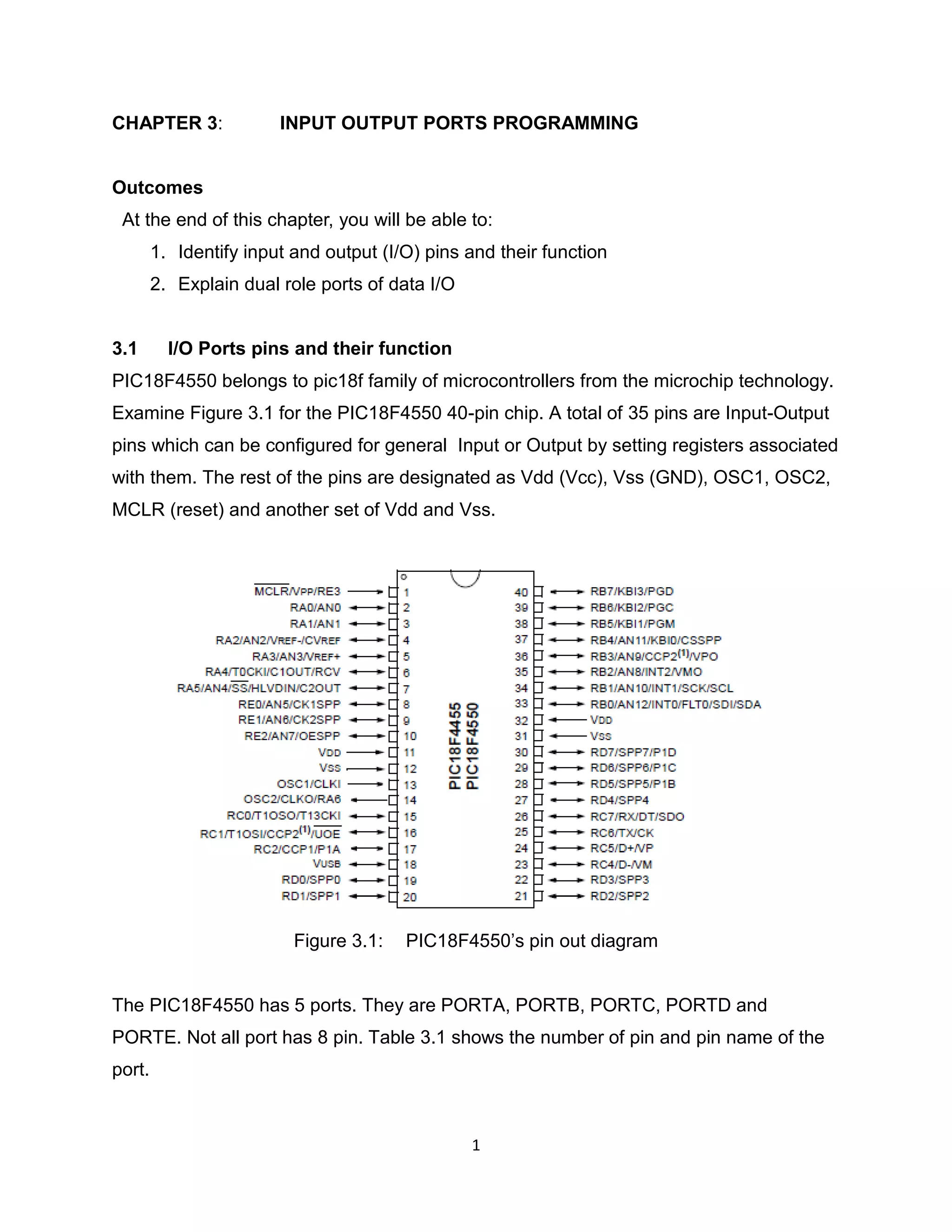


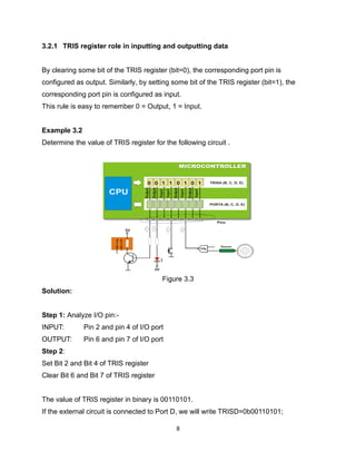

The document discusses input/output (I/O) ports programming for the PIC18F4550 microcontroller. It describes the 5 ports - PORTA, PORTB, PORTC, PORTD, and PORTE, identifying the number of pins in each port. It explains that many pins have dual roles, serving as both general I/O pins and alternate functions. The document outlines how to configure ports as inputs or outputs using TRIS, PORT, and LAT registers. It provides examples of initializing ports and accessing registers by bit or byte to control individual pins.