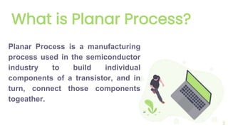
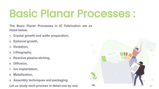
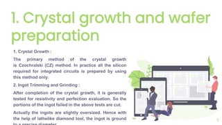
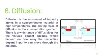
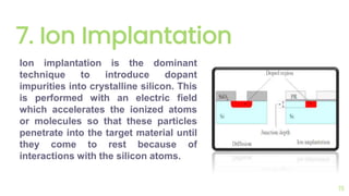
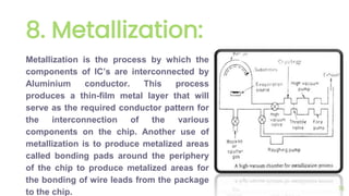
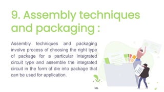
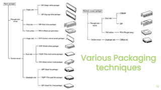
Planar
Fabrication
Technology
By : Prathamesh Gardi
What is Planar Process?
Planar Process is a manufacturing
process used in the semiconductor
industry to build individual
components of a transistor, and in
turn, connect those components
togeather.
2
Basic Planar Processes :
The Basic Planar Processes in IC Fabrication are as
listed below.
1. Crystal growth and wafer preparation,
2. Epitaxial growth,
3. Oxidation,
4. Lithography,
5. Reactive plasma etching,
6. Diffusion,
7. Ion implantation,
8. Metallization,
9. Assembly techniques and packaging
Let us study each process in detail one by one.
1. Crystal growth and wafer
preparation
In this Basic Planar Process in IC Fabrication following
subprocesses, are involved –
● Crystal growing
● Ingot trimming and grinding
● Ingot slicing
● Wafer etching
● Wafer polishing
● Wafer cleaning
4
1. Crystal growth and wafer
preparation
1. Crystal Growth :
The primary method of the crystal growth
is Czochralski (CZ) method. In practice all the silicon
required for integrated circuits is prepared by using
this method only.
2. Ingot Trimming and Grinding :
After completion of the crystal growth, it is generally
tested for resistivity and perfection evaluation. So the
portions of the ingot failed in the above tests are cut.
Actually the ingots are slightly oversized. Hence with
the help of lathelike diamond tool, the ingot is ground 5
1. Crystal growth and wafer
preparation
3. Ingot Slicing :
Once the flats have been ground, the ingot is sliced
into wafers. This Basic Planar Process in IC
Fabrication is very important because it is necessary
to maintain the flat plane and desired surface
orientations.
4. Wafer etching:
Etching is used in microfabrication to chemically
remove layers from the surface of
a wafer during manufacturing. Etching is a critically
important process module, and every wafer undergoes
many etching steps before it is complete. 6
1. Crystal growth and wafer
preparation
5. Wafer Polishing :
After etching, the wafer is polished to eliminate the
microcracks and debris. The main intension of
polishing a wafer is to provide a smooth and perfect
flat surface such that the device features can be
engraved.
6. Wafer Cleaning :
The silicon wafers are cleaned using chemicals.
Generally organic films, heavy metals are deposited on
the surface of the wafers. Hence by using HC1 – H202
aqueous solution, metallic impurities can be removed.
7
2. Epitaxial Growth :
The epitaxy means ‘arranged upon’. In
epitaxy a monocrystalline film is
formed on the top of a monocrystalline
surface. Thus epitaxy is crystalline
growth process in which the
foundation layer i.e. substrate works
as seed crystal. The epitaxial layer
formed on the substrate may be either
n-doped, p-doped or intrinsic.
2. Epitaxial Growth :
There are two types of epitaxy as
given below.
1. Homoepitaxy : When the epitaxial
layer and the substrate on which the
epitaxial layer is to be formed, are of
same materials, then the process is
called The silicon process in which
silicon is grown or formed over
silicon substrate is an example of
homoepitaxy.
2. Epitaxial Growth :
2. Heteroepitaxy : When the epitaxial
layer and the substrate on which the
epitaxial layer is to be formed are not
of identical material, then the process
is called heteroepitaxy. But for
crystalline growth with heteroepitaxy,
the materials must have identical
crystal structure.
10
3. Oxidation
11
Oxidation is a process which converts
silicon on the wafer into silicon
dioxide. For an effective oxidation rate
the wafer must be settled to a furnace
with oxygen or water vapor at
elevated temperatures. Silicon dioxide
layers are used as high-quality
insulators or masks for ion
implantation. The ability of silicon to
form high quality silicon dioxide is an
important reason, why silicon is still
the dominating material
in IC fabrication.
4. Lithography:
12
Lithography is used to transfer a
pattern from a photomask to the
surface of the wafer. For example the
gate area of a MOS transistor is defined
by a specific pattern. The pattern
information is recorded on a layer of
photoresist which is applied on the top
of the wafer.
5. Reactive Plasma Etching:
13
Plasma etching is a form of plasma
processing used to fabricate integrated
circuits. It involves a high-speed stream of
glow discharge (plasma) of an appropriate
gas mixture being shot (in pulses) at a
sample. The plasma source, known as etch
species, can be either charged (ions) or
neutral (atoms and radicals). During the
process, the plasma generates volatile etch
products at room temperature from
the chemical reactions between the elements
of the material etched and the reactive
species generated by the plasma.
6. Diffusion:
14
Diffusion is the movement of impurity
atoms in a semiconductor material at
high temperatures. The driving force of
diffusion is the concentration gradient.
There is a wide range of diffusivities for
the various dopant species, which
depend on how easy the respective
dopant impurity can move through the
material.
7. Ion Implantation
15
Ion implantation is the dominant
technique to introduce dopant
impurities into crystalline silicon. This
is performed with an electric field
which accelerates the ionized atoms
or molecules so that these particles
penetrate into the target material until
they come to rest because of
interactions with the silicon atoms.
8. Metallization:
16
Metallization is the process by which the
components of IC’s are interconnected by
Aluminium conductor. This process
produces a thin-film metal layer that will
serve as the required conductor pattern for
the interconnection of the various
components on the chip. Another use of
metallization is to produce metalized areas
called bonding pads around the periphery
of the chip to produce metalized areas for
the bonding of wire leads from the package
to the chip.
9. Assembly techniques
and packaging :
Assembly techniques and packaging
involve process of choosing the right type
of package for a particular integrated
circuit type and assemble the integrated
circuit in the form of die into package that
can be used for application.
18
Various Packaging
techniques
19

Planar fabrication technology

  • 1.
  • 2.
    What is PlanarProcess? Planar Process is a manufacturing process used in the semiconductor industry to build individual components of a transistor, and in turn, connect those components togeather. 2
  • 3.
    Basic Planar Processes: The Basic Planar Processes in IC Fabrication are as listed below. 1. Crystal growth and wafer preparation, 2. Epitaxial growth, 3. Oxidation, 4. Lithography, 5. Reactive plasma etching, 6. Diffusion, 7. Ion implantation, 8. Metallization, 9. Assembly techniques and packaging Let us study each process in detail one by one.
  • 4.
    1. Crystal growthand wafer preparation In this Basic Planar Process in IC Fabrication following subprocesses, are involved – ● Crystal growing ● Ingot trimming and grinding ● Ingot slicing ● Wafer etching ● Wafer polishing ● Wafer cleaning 4
  • 5.
    1. Crystal growthand wafer preparation 1. Crystal Growth : The primary method of the crystal growth is Czochralski (CZ) method. In practice all the silicon required for integrated circuits is prepared by using this method only. 2. Ingot Trimming and Grinding : After completion of the crystal growth, it is generally tested for resistivity and perfection evaluation. So the portions of the ingot failed in the above tests are cut. Actually the ingots are slightly oversized. Hence with the help of lathelike diamond tool, the ingot is ground 5
  • 6.
    1. Crystal growthand wafer preparation 3. Ingot Slicing : Once the flats have been ground, the ingot is sliced into wafers. This Basic Planar Process in IC Fabrication is very important because it is necessary to maintain the flat plane and desired surface orientations. 4. Wafer etching: Etching is used in microfabrication to chemically remove layers from the surface of a wafer during manufacturing. Etching is a critically important process module, and every wafer undergoes many etching steps before it is complete. 6
  • 7.
    1. Crystal growthand wafer preparation 5. Wafer Polishing : After etching, the wafer is polished to eliminate the microcracks and debris. The main intension of polishing a wafer is to provide a smooth and perfect flat surface such that the device features can be engraved. 6. Wafer Cleaning : The silicon wafers are cleaned using chemicals. Generally organic films, heavy metals are deposited on the surface of the wafers. Hence by using HC1 – H202 aqueous solution, metallic impurities can be removed. 7
  • 8.
    2. Epitaxial Growth: The epitaxy means ‘arranged upon’. In epitaxy a monocrystalline film is formed on the top of a monocrystalline surface. Thus epitaxy is crystalline growth process in which the foundation layer i.e. substrate works as seed crystal. The epitaxial layer formed on the substrate may be either n-doped, p-doped or intrinsic.
  • 9.
    2. Epitaxial Growth: There are two types of epitaxy as given below. 1. Homoepitaxy : When the epitaxial layer and the substrate on which the epitaxial layer is to be formed, are of same materials, then the process is called The silicon process in which silicon is grown or formed over silicon substrate is an example of homoepitaxy.
  • 10.
    2. Epitaxial Growth: 2. Heteroepitaxy : When the epitaxial layer and the substrate on which the epitaxial layer is to be formed are not of identical material, then the process is called heteroepitaxy. But for crystalline growth with heteroepitaxy, the materials must have identical crystal structure. 10
  • 11.
    3. Oxidation 11 Oxidation isa process which converts silicon on the wafer into silicon dioxide. For an effective oxidation rate the wafer must be settled to a furnace with oxygen or water vapor at elevated temperatures. Silicon dioxide layers are used as high-quality insulators or masks for ion implantation. The ability of silicon to form high quality silicon dioxide is an important reason, why silicon is still the dominating material in IC fabrication.
  • 12.
    4. Lithography: 12 Lithography isused to transfer a pattern from a photomask to the surface of the wafer. For example the gate area of a MOS transistor is defined by a specific pattern. The pattern information is recorded on a layer of photoresist which is applied on the top of the wafer.
  • 13.
    5. Reactive PlasmaEtching: 13 Plasma etching is a form of plasma processing used to fabricate integrated circuits. It involves a high-speed stream of glow discharge (plasma) of an appropriate gas mixture being shot (in pulses) at a sample. The plasma source, known as etch species, can be either charged (ions) or neutral (atoms and radicals). During the process, the plasma generates volatile etch products at room temperature from the chemical reactions between the elements of the material etched and the reactive species generated by the plasma.
  • 14.
    6. Diffusion: 14 Diffusion isthe movement of impurity atoms in a semiconductor material at high temperatures. The driving force of diffusion is the concentration gradient. There is a wide range of diffusivities for the various dopant species, which depend on how easy the respective dopant impurity can move through the material.
  • 15.
    7. Ion Implantation 15 Ionimplantation is the dominant technique to introduce dopant impurities into crystalline silicon. This is performed with an electric field which accelerates the ionized atoms or molecules so that these particles penetrate into the target material until they come to rest because of interactions with the silicon atoms.
  • 16.
    8. Metallization: 16 Metallization isthe process by which the components of IC’s are interconnected by Aluminium conductor. This process produces a thin-film metal layer that will serve as the required conductor pattern for the interconnection of the various components on the chip. Another use of metallization is to produce metalized areas called bonding pads around the periphery of the chip to produce metalized areas for the bonding of wire leads from the package to the chip.
  • 17.
    9. Assembly techniques andpackaging : Assembly techniques and packaging involve process of choosing the right type of package for a particular integrated circuit type and assemble the integrated circuit in the form of die into package that can be used for application.
  • 18.
  • 19.