Downloaded 115 times
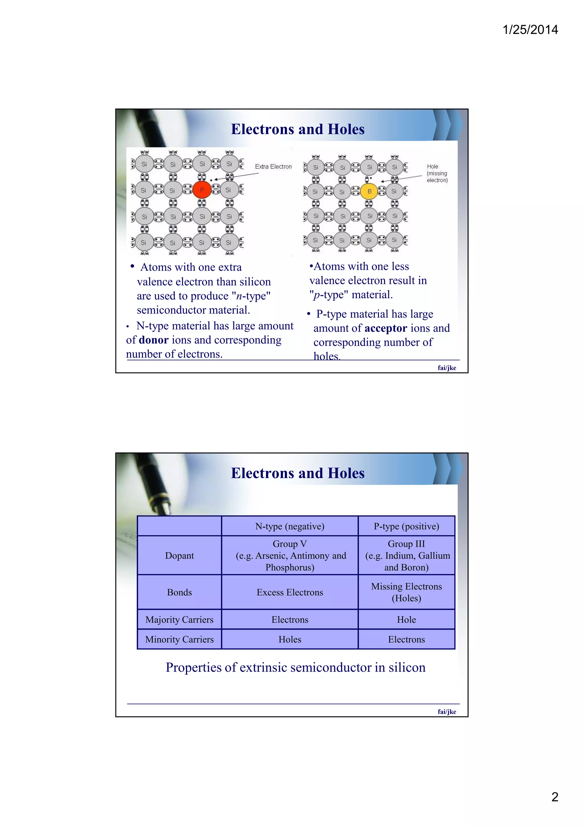
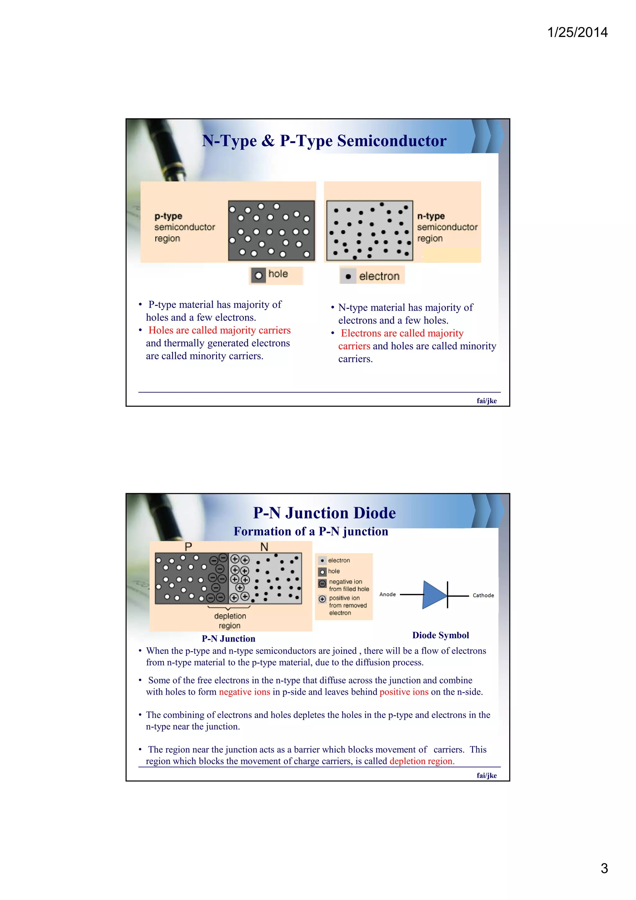
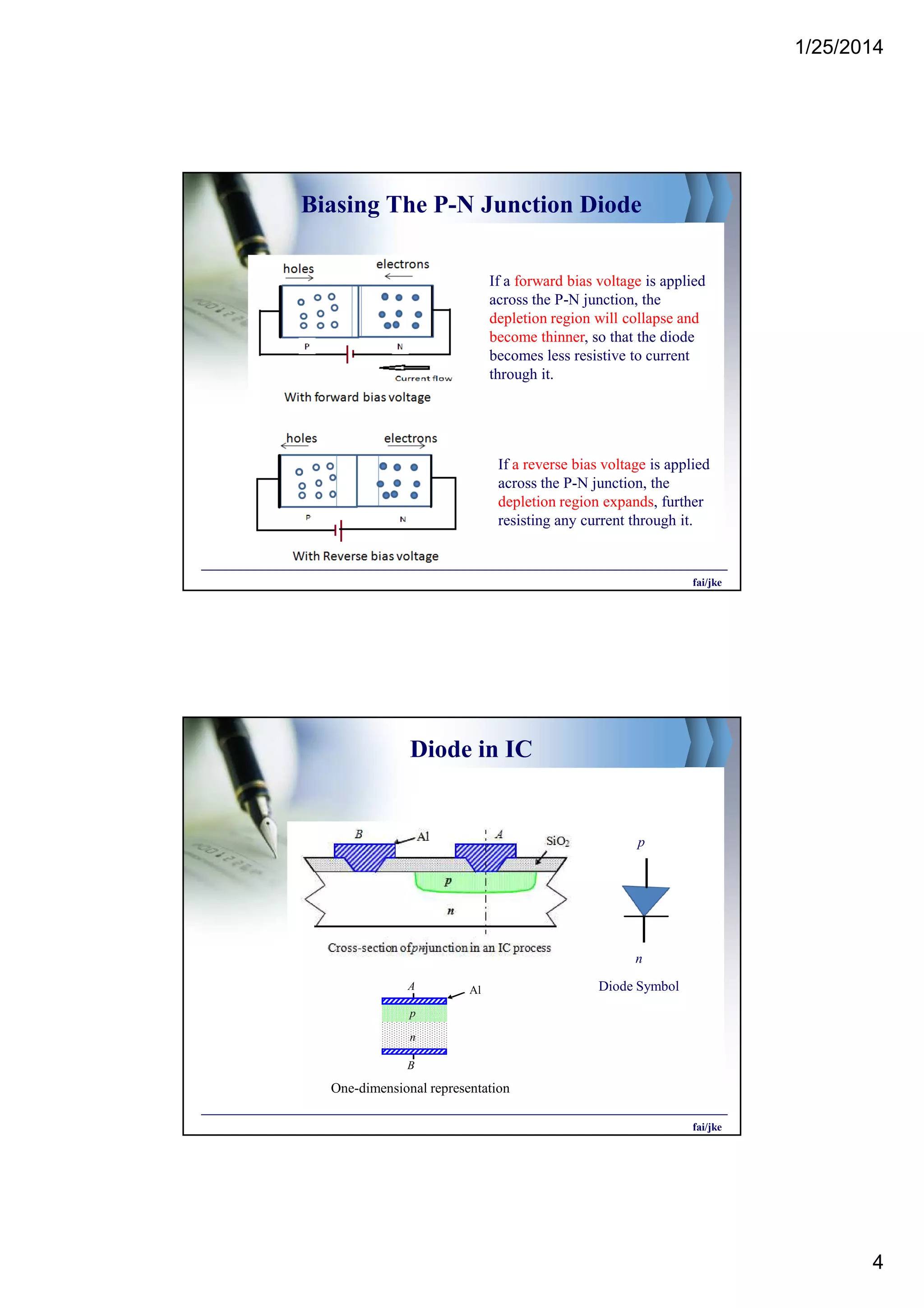
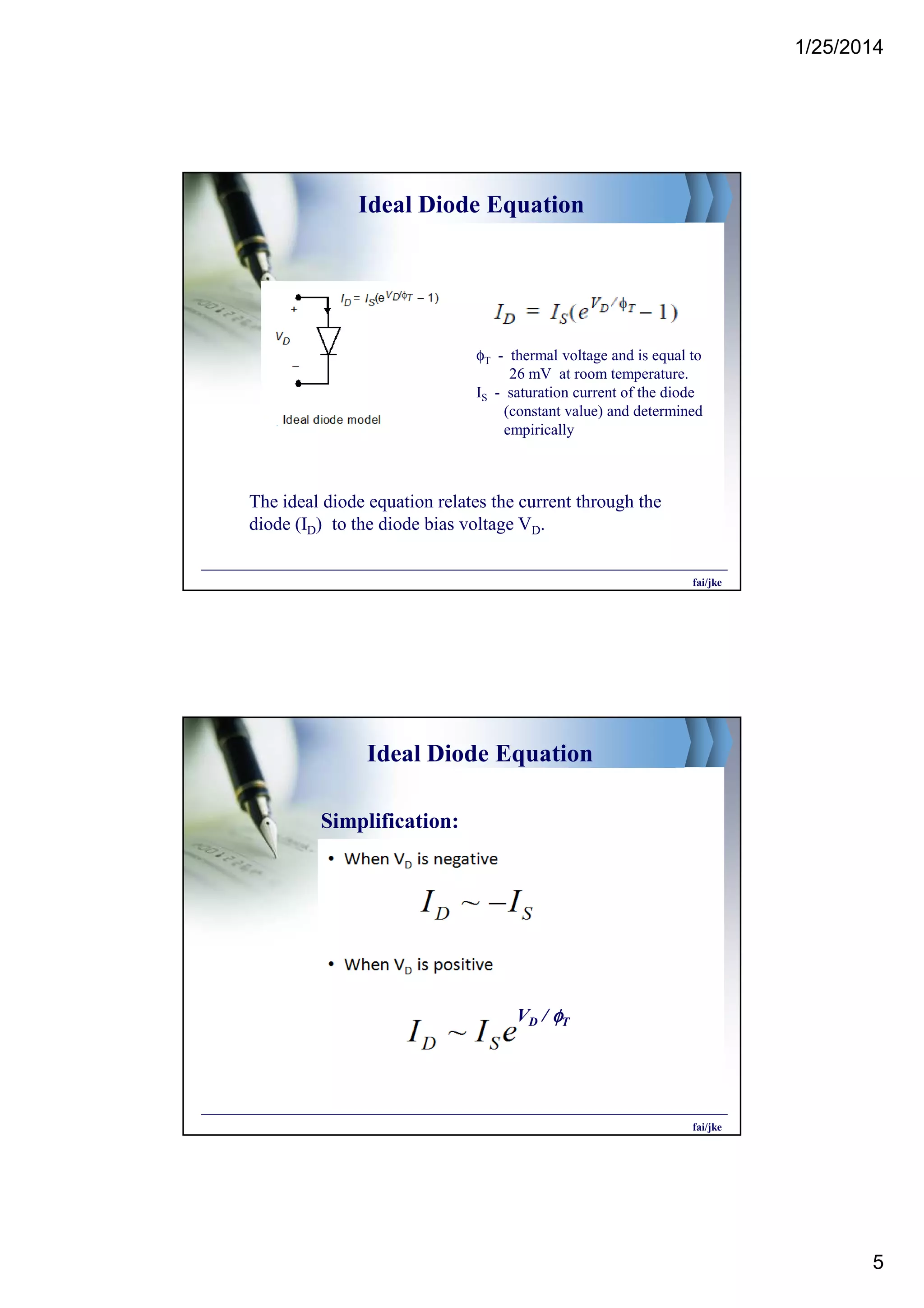
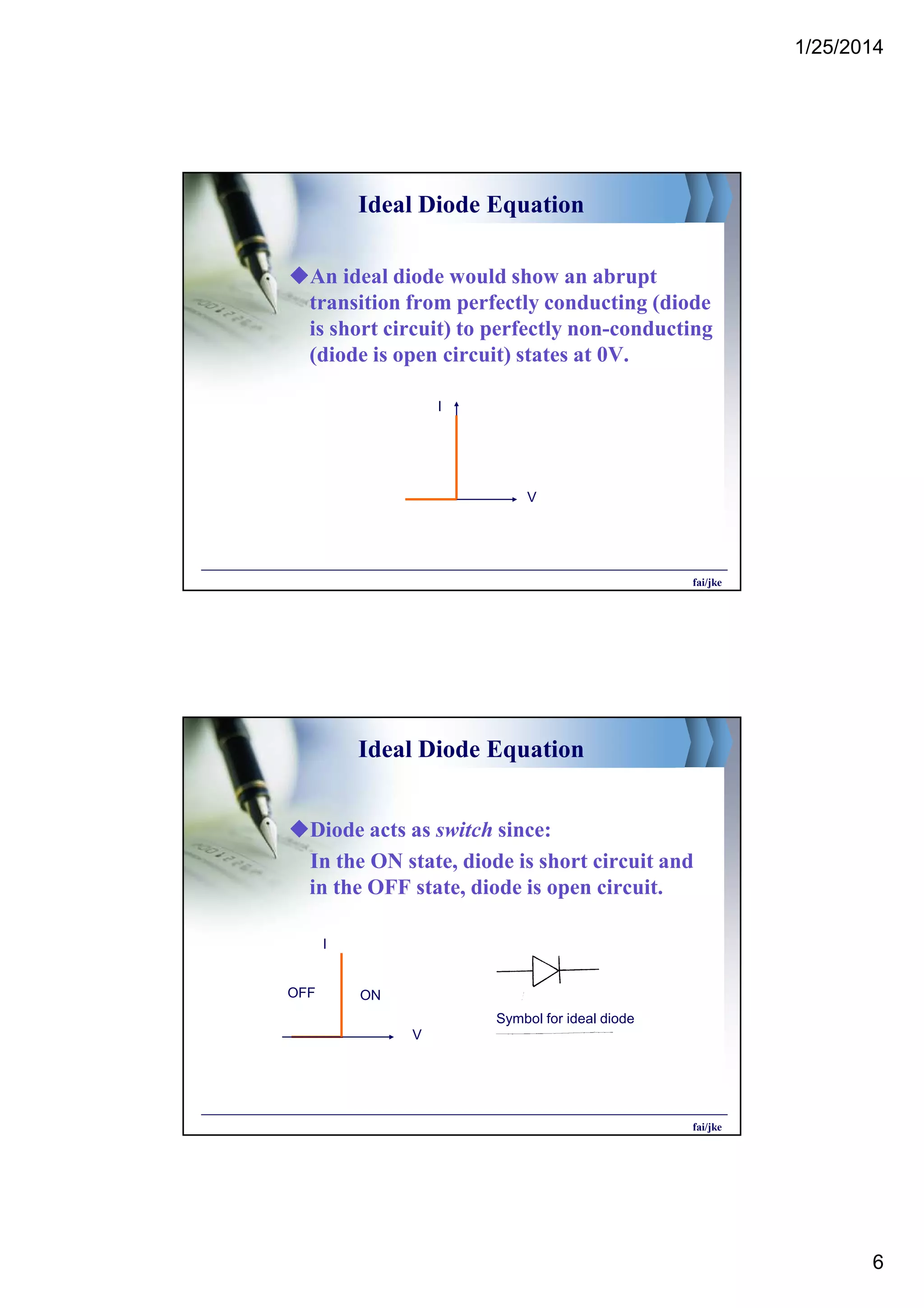
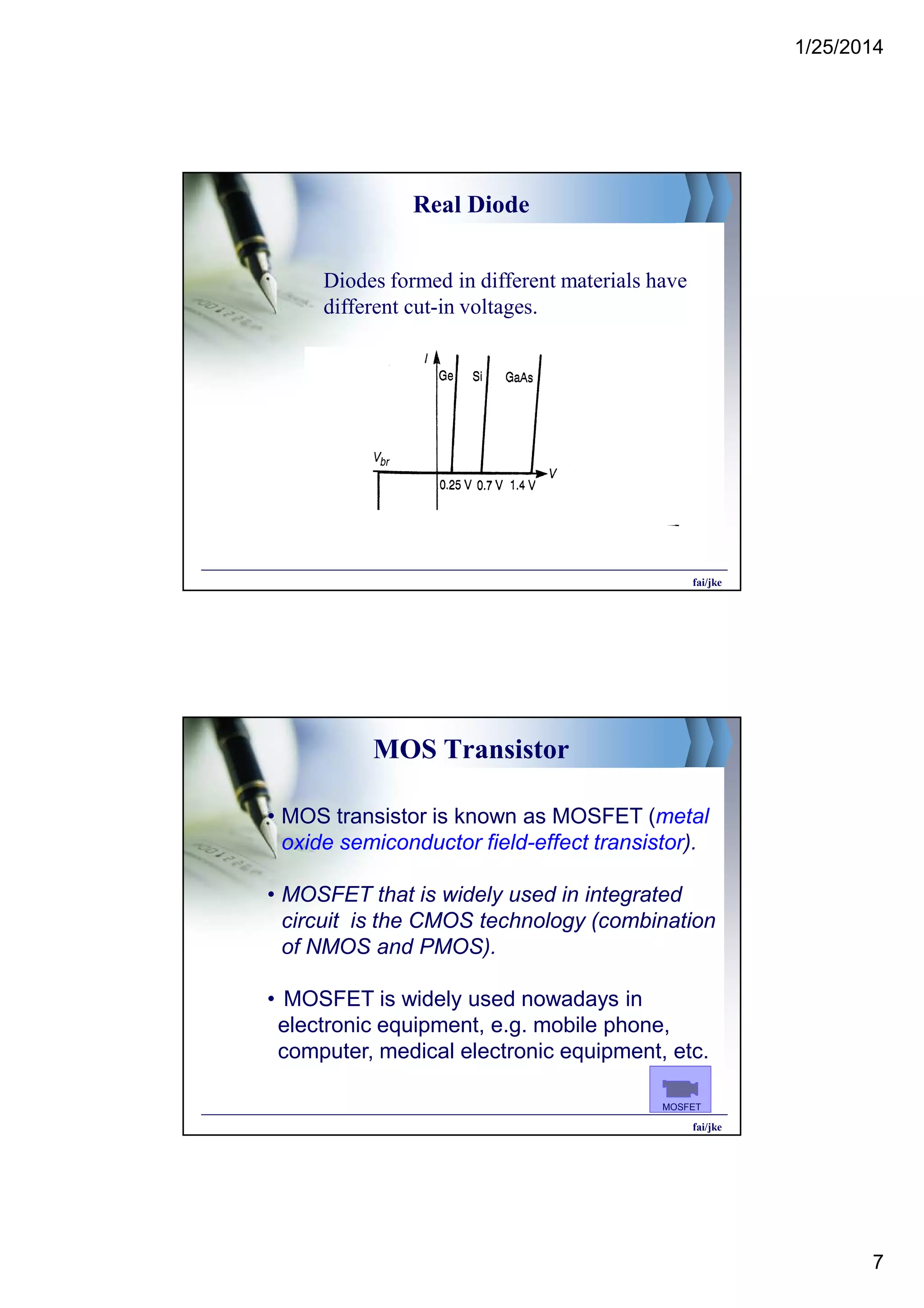
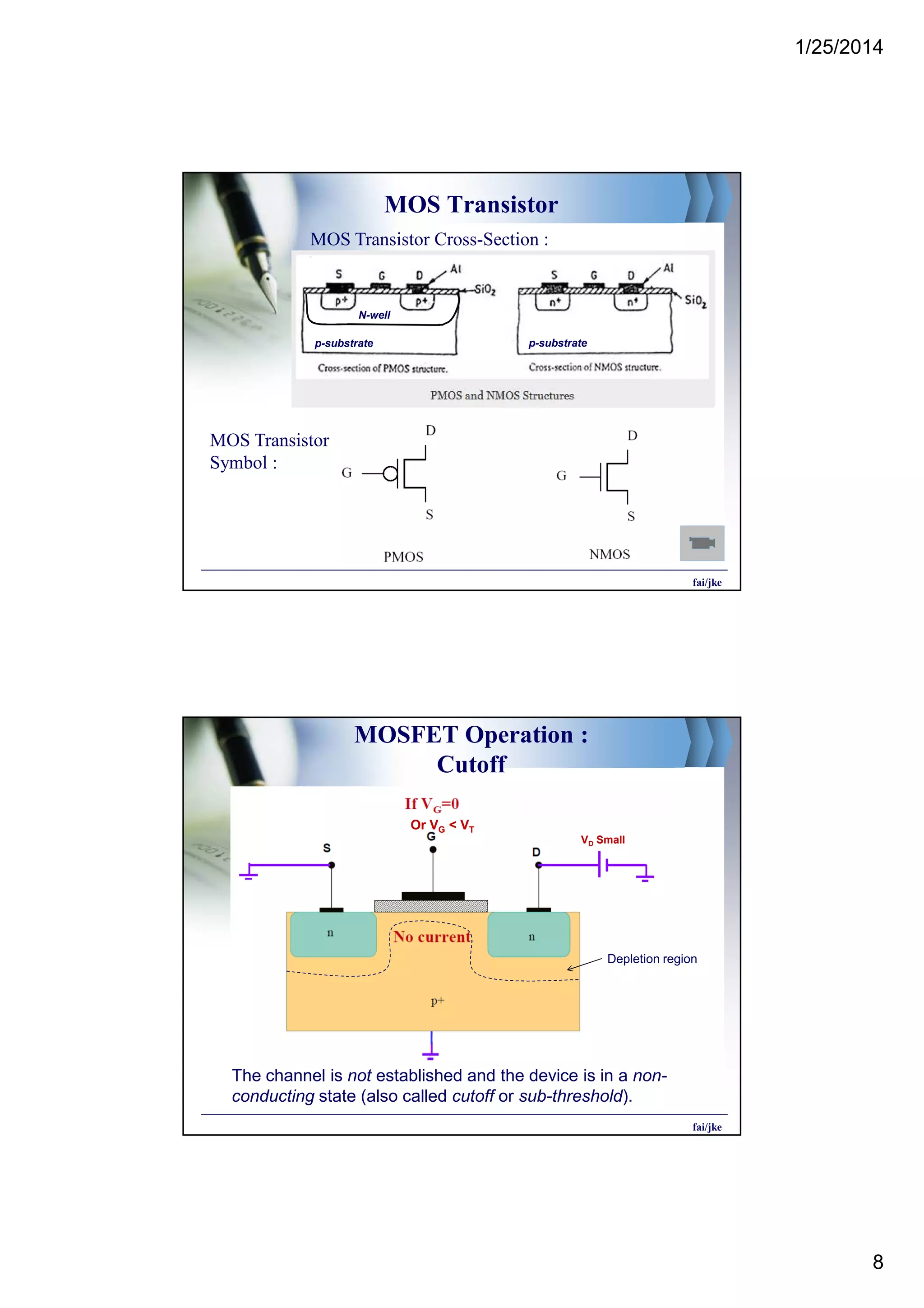
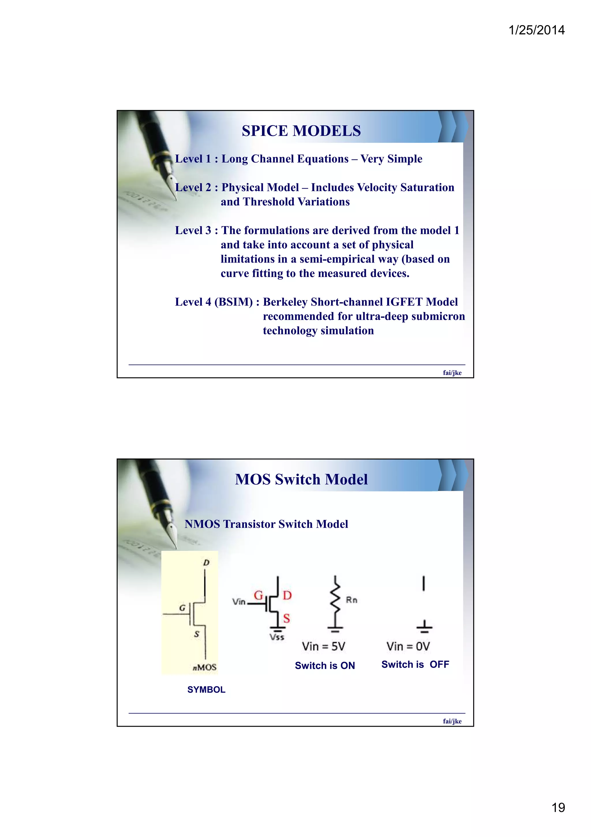
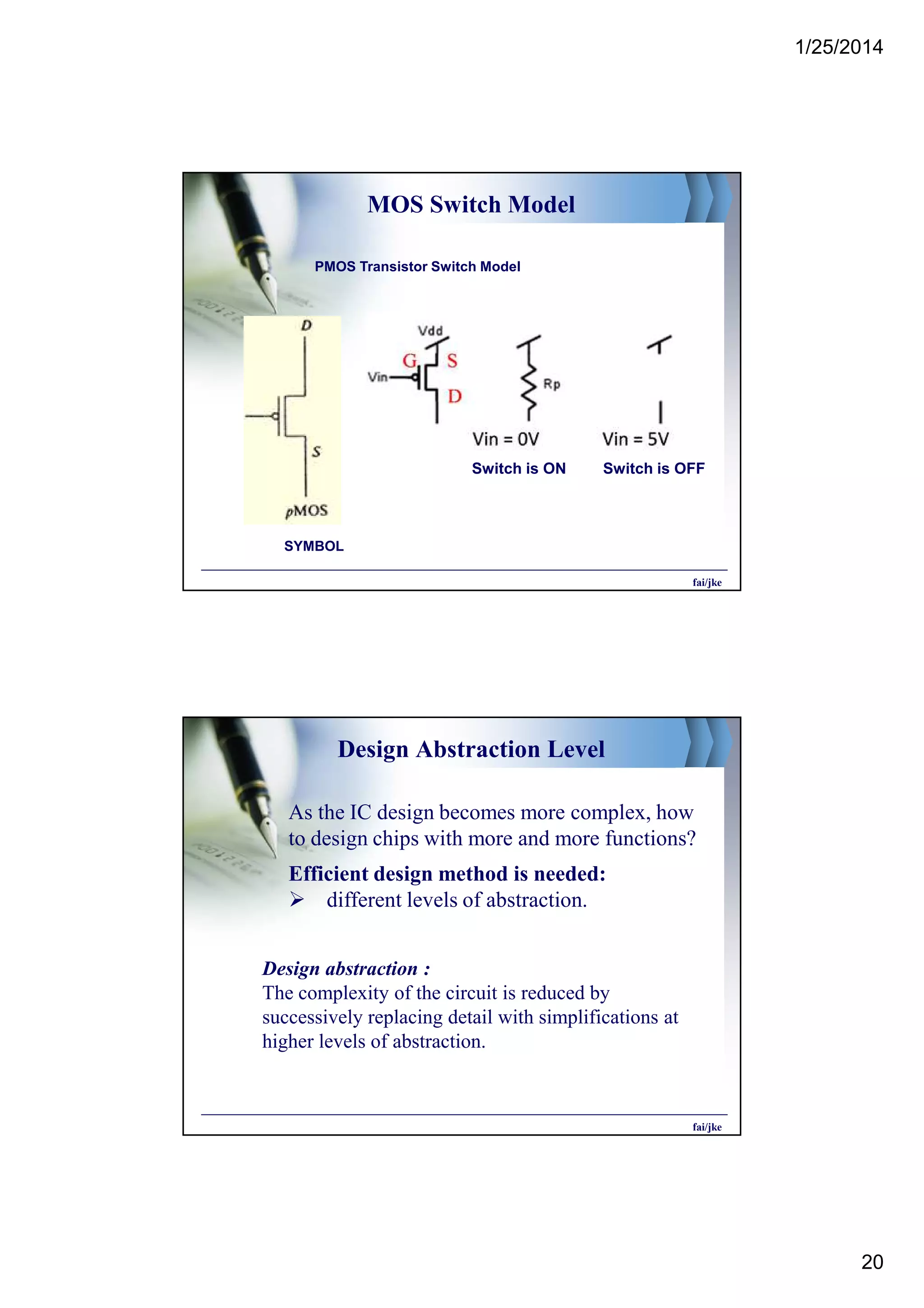
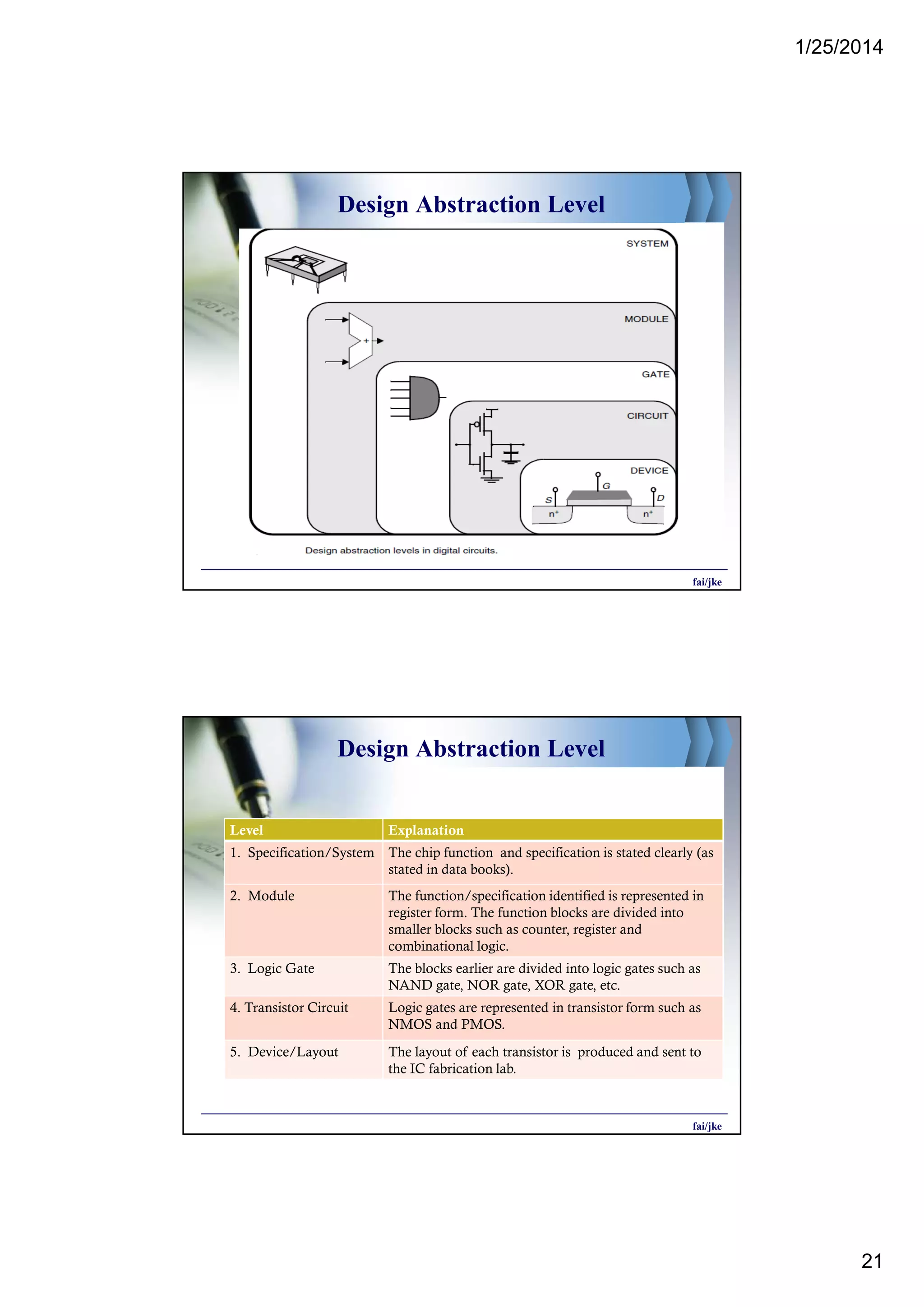


1. The document discusses the basic concepts of diodes and MOS transistors, including their structures, operations, and issues related to submicron MOS transistors. It covers topics such as p-type and n-type semiconductors, the PN junction, biasing of diodes, ideal and real diode equations, MOS transistor structure and operation, and effects in submicron transistors like channel length modulation and velocity saturation. 2. Design abstraction levels are introduced to efficiently design complex ICs through successive simplification and representation of circuits from the system level down to the transistor and layout levels. 3. MOS transistor models like the switch model and SPICE models are presented to simulate and analyze


