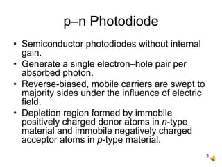
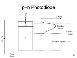
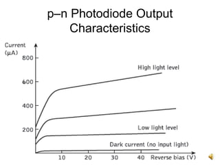
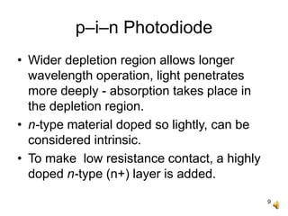
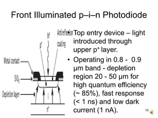
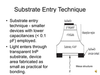
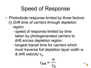
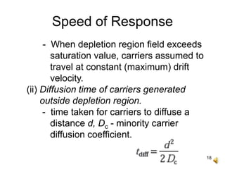
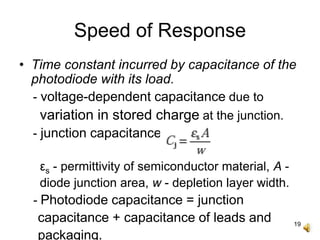
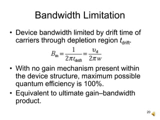
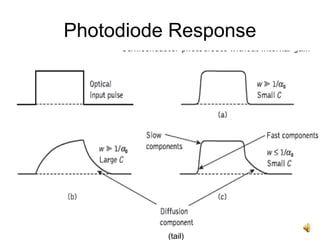
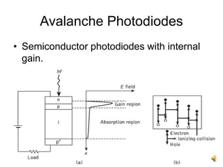
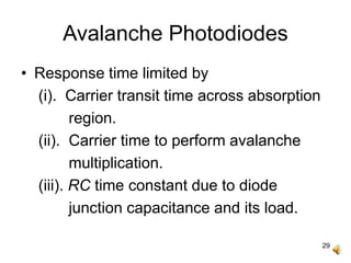
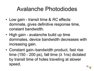
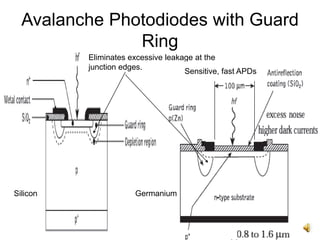
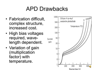
1
Semiconductor Photodiodes
MEC
2
Contents
• Types of Photodiodes.
• PN Junction Photodiodes.
• PIN Photodiodes.
• Avalanche Photodiodes.
• Merits and Demerits.
• Construction and Response.
3
p–n Photodiode
• Semiconductor photodiodes without internal
gain.
• Generate a single electron–hole pair per
absorbed photon.
• Reverse-biased, mobile carriers are swept to
majority sides under the influence of electric
field.
• Depletion region formed by immobile
positively charged donor atoms in n-type
material and immobile negatively charged
acceptor atoms in p-type material.
4
p–n Photodiode
5
p–n Photodiode
• Width of depletion region dependent upon
doping concentrations for a given applied
reverse bias.
• Lower the doping, wider the depletion region.
• Photons may be absorbed in both the
depletion and diffusion regions.
• Absorption region’s position and width
depend upon energy of the incident photons
and on the material.
6
p–n Photodiode
• For weak photon absorption, absorption
region may extend completely throughout
the device.
• Electron–hole pairs generated in both
depletion and diffusion regions.
• In depletion region carrier pairs separate
and drift under electric field, outside this
region the hole diffuses towards the
depletion region to be collected.
7
p–n Photodiode
• Slow diffusion limits photodiode response,
hence photons to be absorbed in the
depletion region.
• Depletion region made long by decreasing
the doping in n-type material.
• Depletion region width is normally 1 to 3 μm,
optimized for efficient detection of light at a
given wavelength - silicon devices in the
visible spectrum(0.4 - 0.7 μm), germanium in
the near infrared (0.7 to 0.9 μm).
8
p–n Photodiode Output
Characteristics
9
p–i–n Photodiode
• Wider depletion region allows longer
wavelength operation, light penetrates
more deeply - absorption takes place in
the depletion region.
• n-type material doped so lightly, can be
considered intrinsic.
• To make low resistance contact, a highly
doped n-type (n+) layer is added.
10
Front Illuminated p–i–n Photodiode
• Top entry device – light
introduced through
upper p+ layer.
• Operating in 0.8 - 0.9
μm band - depletion
region 20 - 50 μm for
high quantum efficiency
(~ 85%), fast response
(< 1 ns) and low dark
current (1 nA).
11
Front Illuminated p–i–n Photodiode
• Dark current from surface leakage
currents and generation–recombination
currents in depletion region without
illumination.
• Quantum efficiency penalty from optical
absorption in undepleted p+-region.
• Limits to how small the device can be
fabricated - light access and metallic
contact on the top.
12
Substrate Entry Technique
• Substrate entry
technique - smaller
devices with lower
capacitances (< 0.1
pF) employed.
• Light enters through
transparent InP
substrate, device
area fabricated as
small as practical for
bonding.
Mesa structure
13
Substrate Entry p-i-n Photodiode
• Also called as back illumination.
• Mesa structure* reduces parasitic
capacitances, dark currents < 1 nA.
• p+-InGaAsP layer heterojunction structure
(Schottky barrier) improves quantum
efficiency (75 - 100 %).
• Charge trapping can occur at the n−p+-
InGaAs/InGaAsP interface – limits the
response time of the device.
14
Side Illuminated p-i-n Photodiode
• Light injected parallel to
the junction plane.
• Large absorption width
(500 μm).
• Sensitive at wavelength
near to bandgap limit
(1.09 μm) where
absorption coefficient is
relatively small.
15
Planar InGaAs p–i–n Photodiode
• Incident light
absorbed in low-
doped n-type InGaAs
layer generating
carriers.
• Discontinuity due to
homojunction b/w n+-
InP substrate & n-
InGaAs absorption
region reduced by
including n-type InP
buffer layer.
16
Planar InGaAs p–i–n Photodiode
Charge trapping
Energy Band Diagram
17
Speed of Response
• Photodiode response limited by three factors:
(i) Drift time of carriers through depletion
region.
- speed of response limited by time
taken by photogenerated carriers to
drift across depletion region.
- longest transit time for carriers which
must traverse full depletion layer width w
& drift velocity vd.
18
Speed of Response
- When depletion region field exceeds
saturation value, carriers assumed to
travel at constant (maximum) drift
velocity.
(ii) Diffusion time of carriers generated
outside depletion region.
- time taken for carriers to diffuse a
distance d, Dc - minority carrier
diffusion coefficient.
19
Speed of Response
• Time constant incurred by capacitance of the
photodiode with its load.
- voltage-dependent capacitance due to
variation in stored charge at the junction.
- junction capacitance
εs - permittivity of semiconductor material, A -
diode junction area, w - depletion layer width.
- Photodiode capacitance = junction
capacitance + capacitance of leads and
packaging.
20
Bandwidth Limitation
• Device bandwidth limited by drift time of
carriers through depletion region tdrift.
• With no gain mechanism present within
the device structure, maximum possible
quantum efficiency is 100%.
• Equivalent to ultimate gain–bandwidth
product.
21
Photodiode Response
(tail)
22
Photodiode Response
• To obtain high quantum efficiency, width
of depletion layer to be far greater than
reciprocal of absorption coefficient for the
material used to fabricate the detector.
• Most of the incident light absorbed,
negligible diffusion outside depletion
region.
• Detector capacitance larger - speed of
response limited by the RC time constant.
23
Photodiode Response
• Output pulse displays a long tail due to
diffusion component to input optical pulse.
• Devices with very thin depletion layers tend
to exhibit distinctive fast response and slow
response components to their output pulses.
• To reduce RC time constant limitation, use
traveling-wave photodiode - absorption and
carrier drift regions positioned orthogonally to
each other.
24
Noise – Dark current
• Photogenerated current due to background
radiation entering the device - dark current
with no intended optical signal present.
• Dark current minimized through use of high-
quality, defect-free material - reduces number
of carriers generated in depletion region and
those which diffuse into this layer from the p−-
and n+- regions.
• Surface currents minimized by careful
fabrication & surface passivation, surface
state & impurity ion concentrations reduced.
25
Avalanche Photodiodes
• Semiconductor photodiodes with internal
gain.
26
Avalanche Photodiodes
• Most of the photons absorbed and primary
carrier pairs generated in depletion region.
• Impact ionization - high-field region in which
holes and electrons acquire sufficient energy
to excite new electron–hole pairs – avalanche
breakdown.
• High reverse bias (50 to 400 V) creates new
carriers by impact ionization, can produce
additional carriers by the same mechanism.
27
Avalanche Photodiodes
• Devices which operate at much lower bias
voltages (15 to 25 V) are available.
• Carrier multiplication factors as great as
104 obtained using defect-free materials to
ensure uniformity of carrier multiplication
over entire photosensitive area.
• Excessive leakage at the junction edges
eliminated using a guard ring structure.
28
Avalanche Photodiodes
• Silicon, germanium and InGaAs APDs
available.
• Carriers generated in undepleted material
are collected somewhat slowly by diffusion
process – produces a long ‘diffusion tail’
on a short optical pulse.
• When APD is fully depleted by employing
electric fields in excess of 104 V/m, all
carriers drift at saturation-limited velocities.
29
Avalanche Photodiodes
• Response time limited by
(i). Carrier transit time across absorption
region.
(ii). Carrier time to perform avalanche
multiplication.
(iii). RC time constant due to diode
junction capacitance and its load.
30
Avalanche Photodiodes
• Low gain - transit time & RC effects
dominate, gives definitive response time,
constant bandwidth.
• High gain - avalanche build up time
dominates, device bandwidth decreases with
increasing gain.
• Constant gain–bandwidth product, fast rise
time (150 - 200 ps), fall time (≥ 1ns) dictated
by transit time of holes traveling at slower
speed.
31
Avalanche Photodiodes with Guard
Ring
Eliminates excessive leakage at the
junction edges.
Silicon Germanium
Sensitive, fast APDs
32
APD Advantages
• Detection of very low light levels - gain.
• Multiplication factor is a measure of the
internal gain, (I - total output current, Ip -
primary photocurrent, )
• Increase in sensitivity of 5 to 15 dB over
p–i–n photodiodes.
• Wider dynamic range.
• As single-photon-counting avalanche
detectors.
33
APD Drawbacks
• Fabrication difficult,
complex structure,
increased cost.
• High bias voltages
required, wave-
length dependent.
• Variation of gain
(multiplication
factor) with
temperature.
34
Thank You

Semiconductor photodiodes

  • 1.
  • 2.
    2 Contents • Types ofPhotodiodes. • PN Junction Photodiodes. • PIN Photodiodes. • Avalanche Photodiodes. • Merits and Demerits. • Construction and Response.
  • 3.
    3 p–n Photodiode • Semiconductorphotodiodes without internal gain. • Generate a single electron–hole pair per absorbed photon. • Reverse-biased, mobile carriers are swept to majority sides under the influence of electric field. • Depletion region formed by immobile positively charged donor atoms in n-type material and immobile negatively charged acceptor atoms in p-type material.
  • 4.
  • 5.
    5 p–n Photodiode • Widthof depletion region dependent upon doping concentrations for a given applied reverse bias. • Lower the doping, wider the depletion region. • Photons may be absorbed in both the depletion and diffusion regions. • Absorption region’s position and width depend upon energy of the incident photons and on the material.
  • 6.
    6 p–n Photodiode • Forweak photon absorption, absorption region may extend completely throughout the device. • Electron–hole pairs generated in both depletion and diffusion regions. • In depletion region carrier pairs separate and drift under electric field, outside this region the hole diffuses towards the depletion region to be collected.
  • 7.
    7 p–n Photodiode • Slowdiffusion limits photodiode response, hence photons to be absorbed in the depletion region. • Depletion region made long by decreasing the doping in n-type material. • Depletion region width is normally 1 to 3 μm, optimized for efficient detection of light at a given wavelength - silicon devices in the visible spectrum(0.4 - 0.7 μm), germanium in the near infrared (0.7 to 0.9 μm).
  • 8.
  • 9.
    9 p–i–n Photodiode • Widerdepletion region allows longer wavelength operation, light penetrates more deeply - absorption takes place in the depletion region. • n-type material doped so lightly, can be considered intrinsic. • To make low resistance contact, a highly doped n-type (n+) layer is added.
  • 10.
    10 Front Illuminated p–i–nPhotodiode • Top entry device – light introduced through upper p+ layer. • Operating in 0.8 - 0.9 μm band - depletion region 20 - 50 μm for high quantum efficiency (~ 85%), fast response (< 1 ns) and low dark current (1 nA).
  • 11.
    11 Front Illuminated p–i–nPhotodiode • Dark current from surface leakage currents and generation–recombination currents in depletion region without illumination. • Quantum efficiency penalty from optical absorption in undepleted p+-region. • Limits to how small the device can be fabricated - light access and metallic contact on the top.
  • 12.
    12 Substrate Entry Technique •Substrate entry technique - smaller devices with lower capacitances (< 0.1 pF) employed. • Light enters through transparent InP substrate, device area fabricated as small as practical for bonding. Mesa structure
  • 13.
    13 Substrate Entry p-i-nPhotodiode • Also called as back illumination. • Mesa structure* reduces parasitic capacitances, dark currents < 1 nA. • p+-InGaAsP layer heterojunction structure (Schottky barrier) improves quantum efficiency (75 - 100 %). • Charge trapping can occur at the n−p+- InGaAs/InGaAsP interface – limits the response time of the device.
  • 14.
    14 Side Illuminated p-i-nPhotodiode • Light injected parallel to the junction plane. • Large absorption width (500 μm). • Sensitive at wavelength near to bandgap limit (1.09 μm) where absorption coefficient is relatively small.
  • 15.
    15 Planar InGaAs p–i–nPhotodiode • Incident light absorbed in low- doped n-type InGaAs layer generating carriers. • Discontinuity due to homojunction b/w n+- InP substrate & n- InGaAs absorption region reduced by including n-type InP buffer layer.
  • 16.
    16 Planar InGaAs p–i–nPhotodiode Charge trapping Energy Band Diagram
  • 17.
    17 Speed of Response •Photodiode response limited by three factors: (i) Drift time of carriers through depletion region. - speed of response limited by time taken by photogenerated carriers to drift across depletion region. - longest transit time for carriers which must traverse full depletion layer width w & drift velocity vd.
  • 18.
    18 Speed of Response -When depletion region field exceeds saturation value, carriers assumed to travel at constant (maximum) drift velocity. (ii) Diffusion time of carriers generated outside depletion region. - time taken for carriers to diffuse a distance d, Dc - minority carrier diffusion coefficient.
  • 19.
    19 Speed of Response •Time constant incurred by capacitance of the photodiode with its load. - voltage-dependent capacitance due to variation in stored charge at the junction. - junction capacitance εs - permittivity of semiconductor material, A - diode junction area, w - depletion layer width. - Photodiode capacitance = junction capacitance + capacitance of leads and packaging.
  • 20.
    20 Bandwidth Limitation • Devicebandwidth limited by drift time of carriers through depletion region tdrift. • With no gain mechanism present within the device structure, maximum possible quantum efficiency is 100%. • Equivalent to ultimate gain–bandwidth product.
  • 21.
  • 22.
    22 Photodiode Response • Toobtain high quantum efficiency, width of depletion layer to be far greater than reciprocal of absorption coefficient for the material used to fabricate the detector. • Most of the incident light absorbed, negligible diffusion outside depletion region. • Detector capacitance larger - speed of response limited by the RC time constant.
  • 23.
    23 Photodiode Response • Outputpulse displays a long tail due to diffusion component to input optical pulse. • Devices with very thin depletion layers tend to exhibit distinctive fast response and slow response components to their output pulses. • To reduce RC time constant limitation, use traveling-wave photodiode - absorption and carrier drift regions positioned orthogonally to each other.
  • 24.
    24 Noise – Darkcurrent • Photogenerated current due to background radiation entering the device - dark current with no intended optical signal present. • Dark current minimized through use of high- quality, defect-free material - reduces number of carriers generated in depletion region and those which diffuse into this layer from the p−- and n+- regions. • Surface currents minimized by careful fabrication & surface passivation, surface state & impurity ion concentrations reduced.
  • 25.
    25 Avalanche Photodiodes • Semiconductorphotodiodes with internal gain.
  • 26.
    26 Avalanche Photodiodes • Mostof the photons absorbed and primary carrier pairs generated in depletion region. • Impact ionization - high-field region in which holes and electrons acquire sufficient energy to excite new electron–hole pairs – avalanche breakdown. • High reverse bias (50 to 400 V) creates new carriers by impact ionization, can produce additional carriers by the same mechanism.
  • 27.
    27 Avalanche Photodiodes • Deviceswhich operate at much lower bias voltages (15 to 25 V) are available. • Carrier multiplication factors as great as 104 obtained using defect-free materials to ensure uniformity of carrier multiplication over entire photosensitive area. • Excessive leakage at the junction edges eliminated using a guard ring structure.
  • 28.
    28 Avalanche Photodiodes • Silicon,germanium and InGaAs APDs available. • Carriers generated in undepleted material are collected somewhat slowly by diffusion process – produces a long ‘diffusion tail’ on a short optical pulse. • When APD is fully depleted by employing electric fields in excess of 104 V/m, all carriers drift at saturation-limited velocities.
  • 29.
    29 Avalanche Photodiodes • Responsetime limited by (i). Carrier transit time across absorption region. (ii). Carrier time to perform avalanche multiplication. (iii). RC time constant due to diode junction capacitance and its load.
  • 30.
    30 Avalanche Photodiodes • Lowgain - transit time & RC effects dominate, gives definitive response time, constant bandwidth. • High gain - avalanche build up time dominates, device bandwidth decreases with increasing gain. • Constant gain–bandwidth product, fast rise time (150 - 200 ps), fall time (≥ 1ns) dictated by transit time of holes traveling at slower speed.
  • 31.
    31 Avalanche Photodiodes withGuard Ring Eliminates excessive leakage at the junction edges. Silicon Germanium Sensitive, fast APDs
  • 32.
    32 APD Advantages • Detectionof very low light levels - gain. • Multiplication factor is a measure of the internal gain, (I - total output current, Ip - primary photocurrent, ) • Increase in sensitivity of 5 to 15 dB over p–i–n photodiodes. • Wider dynamic range. • As single-photon-counting avalanche detectors.
  • 33.
    33 APD Drawbacks • Fabricationdifficult, complex structure, increased cost. • High bias voltages required, wave- length dependent. • Variation of gain (multiplication factor) with temperature.
  • 34.