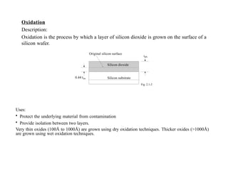
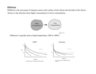
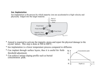
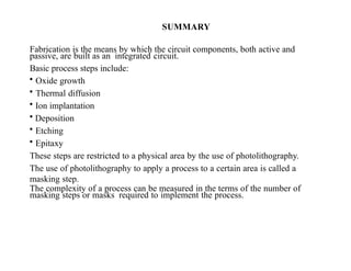
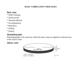
This document provides an introduction to semiconductor manufacturing processes, focusing on integrated circuit fabrication and the various steps involved. Key fabrication steps include wafer cleaning, oxide growth, thermal diffusion, ion implantation, deposition, etching, and epitaxy, often facilitated by photolithography. The document also compares bipolar and CMOS technologies from both analog and digital perspectives, highlighting the advantages of CMOS for large-volume technology driven by digital demands.

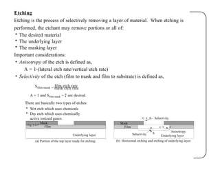
![For Silicon substrate:-
RCA-1 cleaning has been done to remove the organic contaminants from the wafer. 5 parts
of DI water is mixed with 1 part of ammonia solution and 1 part of hydrogen peroxide [a].
RCA-2 cleaning, in which metal ions or thin oxide layer can be removed from it. 6 parts of
DI water along with 1 part of hydrochloric acid and 1 part of hydro peroxide has been used
for this process [a].
[a] Kern, FW. "Cleaning solutions based on hydrogen peroxide for use in silicon semiconductor technology." RCA
Rev. 31 (1970): 187.
Wafer Cleaning](https://image.slidesharecdn.com/unit-6semiconductormanufacturingprocess-230917101730-af41af44-240923030708-c2854054/85/unit-6semiconductormanufacturingprocess-230917101730-af41af44-pptx-5-320.jpg)