Download to read offline


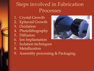


Integrated circuits have increased dramatically in complexity over time due to advances in fabrication technology allowing for higher densities of components on silicon chips. The fabrication process involves growing high purity silicon crystals, depositing layers, doping for conductivity, patterning circuits using photolithography, and packaging individual dies. Advances like shrinking transistor sizes and cleaner room environments have allowed integration to scale while maintaining reliability.


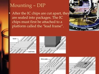
![射頻電子實驗手冊 - [實驗7] 射頻放大器模擬](https://cdn.slidesharecdn.com/ss_thumbnails/simlab7-150613072420-lva1-app6892-thumbnail.jpg?width=640&height=640&fit=bounds)


