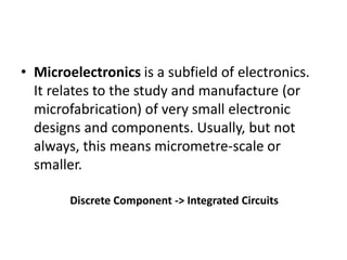
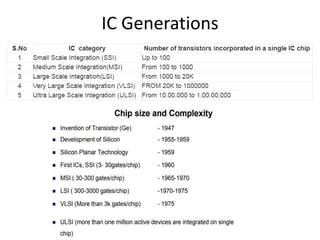
2. • Microelectronics is a subfield of electronics.
It relates to the study and manufacture (or
microfabrication) of very small electronic
designs and components. Usually, but not
always, this means micrometre-scale or
smaller.
Discrete Component -> Integrated Circuits
9. • Monolithic IC: The word ‘monolithic’
(‘mono’+’lithos’)means ‘single stone’ or more appropriately
‘a single-solid structure’. All circuit components, active and
passive, are fabricated inseparably within a single
continuous piece of silicon crystalline material called wafer
(or substrate). Transistors, diodes and other passive
components are fabricated at appropriate spots in the
substrate using epitaxial diffusion techniques.
10. • Thick and Thin Film ICs: These are formed on the
surface of insulating substrate like glass or ceramic
material. Only passive components are formed.
Active elements are added externally (discrete or
monolithic IC).
• Classified not according to their thickness, but
according to processing techniques.
– Thin-film IC: Constructed by depositing films of
conducting material through a mask on the surface.
• Methods: Vacuum evaporation, Cathode sputtering
– Thick-film IC: Silk-screen painting of circuits is
employed. After printing the circuits are high temp.
fired in a furnace to fuse films to the insulating
substrate.
11. • Hybrid or Multichip IC: Circuits are formed
either by interconnecting a number of
individual chips or by a combination of film
and monolithic IC or by a combination of
discrete component and IC.
12. IC Terminologies
• Bonding – attachment of wires to an IC
• Chip /Die – an extremely small part of a silicon wafer on
which IC is fabricated
• Circuit probing – to check the proper electrical
performance of each IC with the help of probes
• Diffusion – introduction of controlled small quantities of
material (dopant atoms/ impurities) into the crystal
structure for modifying its electrical characteristics.
• Photoresist – a photo-sensitive emulsion which hardens
when exposed to ultra-violet light.
• Wafer – a thin slice of a semiconductor material generally
circular in shape in which a number of ICs are fabricated
simultaneously.
13. IC Terminologies….
• Diffusion mask – it is a glass plate with the circuit
pattern drawn on it. Impurities can diffuse through its
transparent areas and not through the opaque ones.
• Encapsulation – putting a cap over the IC and sealing it
in an inert atmosphere.
• Epitaxy – physical placement of materials on a given
surface.
• Etching – chemical removal of surface material from a
chip
• Metallization – providing ohmic contacts and inter-
connections by evaporating aluminium over the chip.
14. IC Fabrication
1. Wafer preparation
2. Epitaxial growth
3. Oxidation
4. Photolithography
5. Isolation diffusion
6. Diffusion (Base/Emitter/Source/Drain etc.)
7. Metallization
8. Circuit probing
9. Scribing and separating into chips
10. Mounting and packing
11. Encapsulation
15. IC Fabrication
1. Wafer preparation
2. Epitaxial growth
3. Oxidation
4. Photolithography
5. Isolation diffusion
6. Diffusion (Base/Emitter/Source/Drain etc.)
7. Metallization
8. Circuit probing
9. Scribing and separating into chips
10. Mounting and packing
11. Encapsulation
17. Silicon ore -> Si single crystal
• Polysilicon ore in molten state
– Single crystal preparation
• Czochralski technique (CZ) - this is the dominant
technique for manufacturing single crystals. It is
especially suited for the large wafers that are currently
used in IC fabrication.
• Float zone technique - this is mainly used for small
sized wafers. The float zone technique is used for
producing specialty wafers that have low oxygen
impurity concentration.
22. IC Fabrication
1. Wafer preparation
2. Epitaxial growth
3. Oxidation
4. Photolithography
5. Isolation diffusion
6. Diffusion (Base/Emitter/Source/Drain etc.)
7. Metallization
8. Circuit probing
9. Scribing and separating into chips
10. Mounting and packing
11. Encapsulation
23. Epitaxial Growth
The word epitaxy derives from the Greek prefix epi meaning
“upon” or “over” and taxis meaning “arrangement” or
“order.” The atoms in an epitaxial layer have a particular
registry (or location) relative to the underlying crystal. The
process results in the formation of crystalline thin films that
may be of the same or different chemical composition and
structure as the substrate and may be composed of only
one or, through repeated depositions, many distinct layers.
24. IC Fabrication
1. Wafer preparation
2. Epitaxial growth
3. Oxidation
4. Photolithography
5. Isolation diffusion
6. Diffusion (Base/Emitter/Source/Drain etc.)
7. Metallization
8. Circuit probing
9. Scribing and separating into chips
10. Mounting and packing
11. Encapsulation
25. Oxidation
Oxidation is a process which converts silicon on the wafer
into silicon dioxide. The chemical reaction of silicon and
oxygen already starts at room temperature but stops after a
very thin native oxide film. For an effective oxidation rate the
wafer must be settled to a furnace with oxygen or water
vapor at elevated temperatures. Silicon dioxide layers are
used as high-quality insulators. The ability of silicon to form
high quality silicon dioxide is an important reason, why
silicon is still the dominating material in IC fabrication.
26. Need of Oxidation
• It is used for surface passivation which is nothing
but creating protective SiO2 layer on the wafer
surface. It protects the junction from moisture
and other atmospheric contaminants.
• It serves as an insulator on the water surface. Its
high relative dielectric constant, which enables
metal line to pass over the active silicon regions.
• It is used to isolate one device from another.
• It forms capacitor with semiconductor on one
side and metal on the other.
27. Types of Oxidation
• Dry oxidation has a lower growth rate than wet oxidation although
the oxide film quality is better than the wet oxide film. Therefore
thin oxides such as screen oxide, pad oxide, and especially gate
oxide normally use the dry oxidation process. Dry oxidation also
results in a higher density oxide than that achieved by wet oxide
and so it has a higher breakdown voltage (5 to 10 MV/cm).
Si + O2 SiO2 -----------------DRY OXIDATION
• In case of wet oxidation where water is use instead of oxygen, the
water molecule can dissociate at high temperatures to form
hydroxide OH that can diffuse in the silicon faster than molecular
O2. Therefore the wet oxidation process has a significantly higher
oxidation rate than the dry oxidation. It is used to grow thick oxides
such as masking oxide, blanket field oxide, and the LOCOS oxide.
Si + 2H2O SiO2 + 2H2--------WET OXIDATION
28. IC Fabrication
1. Wafer preparation
2. Epitaxial growth
3. Oxidation
4. Photolithography
5. Isolation diffusion
6. Diffusion (Base/Emitter/Source/Drain etc.)
7. Metallization
8. Circuit probing
9. Scribing and separating into chips
10. Mounting and packing
11. Encapsulation
29. What is Lithography?
The word lithography comes from the
Greek lithos, meaning stones,
and graphia, meaning to write. It means
quite literally writing on stones. In the
case of semiconductor lithography (also
called photolithography) our stones are
silicon wafers and our patterns are
written with a light sensitive polymer
called a photoresist. To build the
complex structures that make up a
transistor and the many wires that
connect the millions of transistors of a
circuit, lithography and etch pattern
transfer steps are repeated at least 10
times.
30. Prebake: Heating for
proper binding of the
resist with the wafer
Mask
Solubility of exposed
photoresist (PR)
increases and dissolves
in appropriate solvent.
The remaining part of
PR remains and protects
the wafer for exposure
to Etch, Implant,
Diffusion etc.
Ultra Violet radiation
31. IC Fabrication
1. Wafer preparation
2. Epitaxial growth
3. Oxidation
4. Photolithography
5. Isolation diffusion
6. Diffusion (Base/Emitter/Source/Drain etc.)
7. Metallization
8. Circuit probing
9. Scribing and separating into chips
10. Mounting and packing
11. Encapsulation
32. Diffusion
• Diffusion is a process by which atoms move from
a high-concentration region to a low
concentration region. This is very much like a
drop of ink dispersing through a glass of water
except that it occurs much more slowly in solids.
In VLSI fabrication, this is a method to introduce
impurity atoms (dopants) into silicon to change
its resistivity.
• Purpose
– Impurity Doping (Ion implantation is another method)
– Isolation
33. Ion Implantation
• Ion implantation is another method used to introduce
impurities into the semiconductor crystal. An ion implanter
produces ions of the desired dopant, accelerates them by
an electric field, and allows them to strike the
semiconductor surface. The ions become embedded in the
crystal lattice. The depth of penetration is related to the
energy of the ion beam, which can be controlled by the
accelerating-field voltage. The quantity of ions implanted
can be controlled by varying the beam current (flow of
ions). Since both voltage and current can be accurately
measured and controlled, ion implantation results in
impurity profiles that are much more accurate and
reproducible than can be obtained by diffusion.
36. Diffusion for isolation
• Isolation between two adjacent transistors in CMOS circuits is necessary
to isolate n channel and p channel transistors in order to avoid the
undesirable parasitic currents between the transistors.
• The method involves producing regions of n- type material surrounded by
p-type material. Components are then fabricated in different n-type wells.
• The p-type material surrounding the wells is given the most negative p
potential with respect to all parts of the wafer, thus each well and hence
component is electrically isolated from the others by back-to-back diodes.
37. IC Fabrication
1. Wafer preparation
2. Epitaxial growth
3. Oxidation
4. Photolithography
5. Isolation diffusion
6. Diffusion (Base/Emitter/Source/Drain etc.)
7. Metallization
8. Circuit probing
9. Scribing and separating into chips
10. Mounting and packing
11. Encapsulation
38. Metallization
• The purpose of metallization is to
interconnect the various components
(transistors, capacitors, etc.) to form the
desired integrated circuit and to take out
contact leads. Metallization involves the
deposition of a metal over the entire surface
of the silicon. The required interconnection
pattern is then selectively etched. The metal
layer is normally deposited via a sputtering
process.
39. IC Fabrication
1. Wafer preparation
2. Epitaxial growth
3. Oxidation
4. Photolithography
5. Isolation diffusion
6. Diffusion (Base/Emitter/Source/Drain etc.)
7. Metallization
8. Circuit probing
9. Scribing and separating into chips
10. Mounting and packing
11. Encapsulation
40. Packaging
A finished silicon wafer may contain several hundreds of finished circuits or
chips. A chip may contain from 10 to more than 108 transistors; each chip is
rectangular and can be up to tens of millimeters on a side.
• Probing: The circuits are first tested electrically (while still in wafer form)
using an automatic probing station. Bad circuits are marked for later
identification.
• Scribing & separation: The circuits are then separated from each other (by
dicing), and the good circuits (dies) are mounted in packages (headers).
• Interconnect & Packaging: Traditionally, fine gold wires are normally used
to interconnect the pins of the package to the metallization pattern on the
die.
• Encapsulation: Finally, the package is sealed using plastic or epoxy under
vacuum or in an inert atmosphere