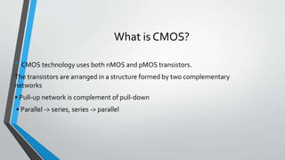
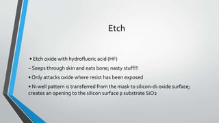
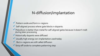
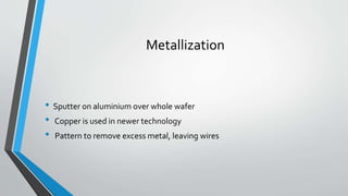
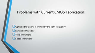
CMOS FABRICATION &
TECHNIQUES
BY- ABHISHEK SUR
INDEX
Overview of CMOS
CMOS Fabrication Process Overview
CMOS Fabrication Process
Problems with Current CMOS Fabrication
Future Changes in CMOS Fabrication
What is CMOS?
• CMOS technology uses both nMOS and pMOS transistors.
The transistors are arranged in a structure formed by two complementary
networks
• Pull-up network is complement of pull-down
• Parallel -> series, series -> parallel
CMOS Fabrication
CMOS transistors are fabricated on silicon wafer
Wafers diameters (200-300 mm)
Lithography process similar to printing press
On each step, different materials are deposited, or patterned or etched.
Easiest to understand by viewing both top and cross-section of wafer in a
simplified manufacturing process.
Inverter Cross-section
•Typically use p-type substrate for nMOS transistors
• Requires to make an n-well for body of pMOS transistors
Inverter Mask Set
•Top view
•Transistors and wires are defined by masks
• Cross-section taken along dashed line
Detailed MaskViews
• Six masks
– n-well
– Polysilicon
– n+ diffusion
– p+ diffusion
– Contact
– Metal
Fabrication Steps
• Start with blank wafer (typically p-type where NMOS is created)
• Build inverter from the bottom up
• First step will be to form the n-well (where PMOS would reside)
– Cover wafer with protective layer of SiO2 (oxide)
– Remove oxide layer where n-well should be built
– Implant or diffuse n dopants into exposed wafer to form n-well
– Strip off SiO2
Oxidation
• Grow SiO2 on top of Si wafer
– (900 – 1200 C )with H2O or O2 in oxidation furnace
PHOTORESIST
• Spin on photoresist
– Photoresist is a light-sensitive organic polymer
– Property changes where exposed to light
•Two types of photoresists (positive or negative)
– Positive resists can be removed if exposed to UV light
– Negative resists cannot be removed if exposed to UV light
Lithography
• Expose photoresist to Ultra-violate (UV) light through the n-well mask
• Strip off exposed photoresist with chemicals
Etch
• Etch oxide with hydrofluoric acid (HF)
– Seeps through skin and eats bone; nasty stuff!!!
• Only attacks oxide where resist has been exposed
• N-well pattern is transferred from the mask to silicon-di-oxide surface;
creates an opening to the silicon surface p substrate SiO2
N-diffusion/implantation
Pattern oxide and form n+ regions
Self-aligned process where gate blocks n-dopants
Polysilicon is better than metal for self-aligned gates because it doesn’t melt
during later processing
Historically dopants were diffused
Usually high energy ion-implantation used today
 But n+ regions are still called diffusion
Strip off oxide to complete patterning step
P-Diffusion/implantation
• Similar set of steps form p+ “diffusion” regions for PMOS source and drain
and substrate contact
CONTACTS
 Now we need to wire together the devices
 Cover chip with thick field oxide (FO)
 Etch oxide where contact cuts are needed
Metallization
• Sputter on aluminium over whole wafer
• Copper is used in newer technology
• Pattern to remove excess metal, leaving wires
Problems with Current CMOS Fabrication
Optical lithography is limited by the light frequency.
Material limitations
Yield limitations
Space limitations
Future Changes in CMOS Fabrication
• Material changes like using high-k materials.
• Design changes – SOI(Silicon On Insulator)
– Double Gate (Finfet)
–Twin-Tub Process
THANKYOU!!

CMOS FABRICATION AND TECHNIQUES

  • 1.
  • 2.
    INDEX Overview of CMOS CMOSFabrication Process Overview CMOS Fabrication Process Problems with Current CMOS Fabrication Future Changes in CMOS Fabrication
  • 3.
    What is CMOS? •CMOS technology uses both nMOS and pMOS transistors. The transistors are arranged in a structure formed by two complementary networks • Pull-up network is complement of pull-down • Parallel -> series, series -> parallel
  • 4.
    CMOS Fabrication CMOS transistorsare fabricated on silicon wafer Wafers diameters (200-300 mm) Lithography process similar to printing press On each step, different materials are deposited, or patterned or etched. Easiest to understand by viewing both top and cross-section of wafer in a simplified manufacturing process.
  • 5.
    Inverter Cross-section •Typically usep-type substrate for nMOS transistors • Requires to make an n-well for body of pMOS transistors
  • 6.
    Inverter Mask Set •Topview •Transistors and wires are defined by masks • Cross-section taken along dashed line
  • 7.
    Detailed MaskViews • Sixmasks – n-well – Polysilicon – n+ diffusion – p+ diffusion – Contact – Metal
  • 8.
    Fabrication Steps • Startwith blank wafer (typically p-type where NMOS is created) • Build inverter from the bottom up • First step will be to form the n-well (where PMOS would reside) – Cover wafer with protective layer of SiO2 (oxide) – Remove oxide layer where n-well should be built – Implant or diffuse n dopants into exposed wafer to form n-well – Strip off SiO2
  • 9.
    Oxidation • Grow SiO2on top of Si wafer – (900 – 1200 C )with H2O or O2 in oxidation furnace
  • 10.
    PHOTORESIST • Spin onphotoresist – Photoresist is a light-sensitive organic polymer – Property changes where exposed to light •Two types of photoresists (positive or negative) – Positive resists can be removed if exposed to UV light – Negative resists cannot be removed if exposed to UV light
  • 11.
    Lithography • Expose photoresistto Ultra-violate (UV) light through the n-well mask • Strip off exposed photoresist with chemicals
  • 12.
    Etch • Etch oxidewith hydrofluoric acid (HF) – Seeps through skin and eats bone; nasty stuff!!! • Only attacks oxide where resist has been exposed • N-well pattern is transferred from the mask to silicon-di-oxide surface; creates an opening to the silicon surface p substrate SiO2
  • 13.
    N-diffusion/implantation Pattern oxide andform n+ regions Self-aligned process where gate blocks n-dopants Polysilicon is better than metal for self-aligned gates because it doesn’t melt during later processing Historically dopants were diffused Usually high energy ion-implantation used today  But n+ regions are still called diffusion Strip off oxide to complete patterning step
  • 14.
    P-Diffusion/implantation • Similar setof steps form p+ “diffusion” regions for PMOS source and drain and substrate contact
  • 15.
    CONTACTS  Now weneed to wire together the devices  Cover chip with thick field oxide (FO)  Etch oxide where contact cuts are needed
  • 16.
    Metallization • Sputter onaluminium over whole wafer • Copper is used in newer technology • Pattern to remove excess metal, leaving wires
  • 17.
    Problems with CurrentCMOS Fabrication Optical lithography is limited by the light frequency. Material limitations Yield limitations Space limitations
  • 18.
    Future Changes inCMOS Fabrication • Material changes like using high-k materials. • Design changes – SOI(Silicon On Insulator) – Double Gate (Finfet) –Twin-Tub Process
  • 19.